Effect of self-consistent electric field on characteristics of graphene p-i-n tunneling transit-time diodes
Abstract
We develop a device model for p-i-n tunneling transit-time diodes based on single- and multiple graphene layer structures operating at the reverse bias voltages. The model of the graphene tunneling transit-time diode (GTUNNETT) accounts for the features of the interband tunneling generation of electrons and holes and their ballistic transport in the device i-section, as well as the effect of the self-consistent electric field associated with the charges of propagating electrons and holes. Using the developed model, we calculate the dc current-voltage characteristics and the small-signal ac frequency-dependent admittance as functions of the GTUNNETT structural parameters , in particular, the number of graphene layers and the dielectric constant of the surrounding media. It is shown that the admittance real part can be negative in a certain frequency range. As revealed, if the i-section somewhat shorter than one micrometer, this range corresponds to the terahertz frequencies. Due to the effect of the self-consistent electric field, the behavior of the GTUNNETT admittance in the range of its negativity of its real part is rather sensitive to the relation between the number of graphene layers and dielectric constant. The obtained results demonstrate that GTUNNETTs with optimized structure can be used in efficient terahertz oscillators.
I Introduction
Pioneering papers by Shur and Eastman 1 ; 2 have stimulated extensive studies (which continue already for the fourth decade) of ballistic electron and hole transport (BET and BHT, respectively), i.e., collision free transport in short semiconductor structures. The main incentive is the realization of fastest velocities of electrons/holes and, hence, achievement of the operation of diodes and transistors in terahertz range (THz) of frequencies and low power consumption. Even at the initial stage of the ballistic transport research, several concepts of ballistic THz sources have been put forward (see, for instance, an early review 3 ). However, the realization THz generation in different semiconductor devices associated with BET/BHT, in particular, analogous to vacuum devices, meets the problems associated with electron scattering in real semiconductor structures. Creation of heterostructures with selective doping with a two-dimensional electron gas (2DEG) spatially separated from the donors, has resulted in achievement of very long mean free path of electrons, at least at low temperatures. Recent discoveries of unique properties of graphene 4 ; 5 , in particular, the demonstration of possibility of very long electron and hole mean free path in graphene layers (GLs) and what is even more interesting in multiple graphene layers (MGLs) 6 ; 7 add optimism in building graphene based THz devices using BET. The concept of graphene tunneling transit-time (GTUNNETT) p-i-n diode , which exhibits a negative dynamic conductivity in the THz range, was proposed and substantiated in Refs. 8 ; 9 . This concept based not only on BET or quasi-BET (as well as BHT or quasi-BHT) in GLs and MGLs, but also on a strong interband tunneling under the electric field with a pronounced anisotropy 10 ; 11 due to the gapless energy spectrum, and constant absolute value of electrons and holes velocities 4 . Due to this, the electrons in the conduction band and the holes in the valence band generated owing to the interband tunneling in the electric field propogate primarily in the electric field direction with the velocity (in this direction) virtually equal to the characteristic velocity cm/s. A large value of the directed velocity in GLs and MGLs promotes the device operation at elevated frequencies.
As shown 8 ; 9 , for the self-excitation of THz oscillations in a circuit with GTUNNETT diode, this circuit should serve as a resonator. However, at elevated tunneling currents in GTUNNETTs considered previously 8 ; 9 the self-consistent charge associated with propagating electron and hole streams can affect the spatial distribution of the self-consistent electric field and the electric potential in the i-section. As a result, the self-consistent electric field near the p-i- and i-n-juctions can be substantially reinforced. This, in turn, influences the tunneling generation of electrons and holes and the their transit conditions and, hence, the GTUNNETT dc and ac characteristics.
In this paper, in contrast to the previous treatment 8 ; 9 , we account for the self-consistent electric field associated with the variations of the electron and hole lateral charges in the i-section and their effect on the injection and the dc and ac characteristics. The effects of the space charge in planar TUNNETTs with the propagation of carriers perpendicular to the structure plane were considered by Gribnikov et al. 12 . The problems of calculation of the dc and ac characteristics of devices based on lateral structures accounting for the self-consistent electric field are substantially complicated by the features of the structure geometry (2D electron and hole channels and blade-like contact regions). In particular, as shown in the following, the related mathematical problems are reduced to a system of rather complex nonlinear integral-differential equations. Using the GTUNNETT device model, we derive these equations, solve them numerically, and find the characteristics.
II Equations of the model
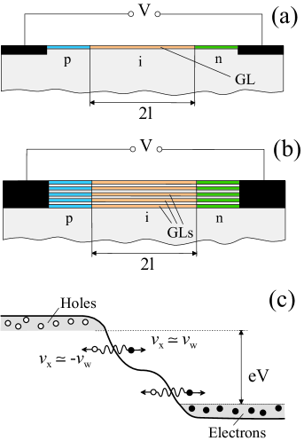
The device under consideration is based on a GL or MGL structures with p- and n- side sections with the contacts and an undoped transit i-section. For definiteness, we assume that p-and n-sections in a GL or in an MGL are created by chemical doping 13 , although in similar devices but with extra gates these sections can be formed electrically 10 ; 11 . Under the reverse bias voltage , the potential drops primarily across the i-section A schematic view of the structures in question and their band-diagram under sufficiently strong reverse bias () corresponding to the potential distribution in the i-section with a markedly nonuniform electric field are shown in Fig. 1.
The electrons and holes injected into the i-section of one GL are characterized by the electron and hole sheet concentrations, and , respectively and the potential . Here the axis is directed along the GL (or MGL) plane, i.e., in the direction of the current, the axis is directed perpendicular to this plane, and is the time. In the general case when the i-section is based on MGL, and are the electron and hole densities in each GLs. In the case of BET and BHT, on which we focus mainly, the electron and hole sheet densities in each GL obey the continuity equations
| (1) |
and the Poisson equation
| (2) |
respectively. Here is the electron charge, is the dielectric constant of the media surrounding GL (or MGL structure), is the number of GLs in the GTUNNETT structure, and is the delta function reflecting a narrowiness of GL and MGL structures even with rather large number of GLs in the direction. Equation (1) corresponds to the situation when the electrons and holes generated due to the interband tunneling in the i-section obtain the directed velocities and and preserve them during the propagation. The boundary conditions correspond to the assumption that the electrons and holes appear in the i-section only due to the interband tunneling (the injection of electrons from the p-section and holes from the n-section is negligible) and that the highly conducting side contacts to the p- and n-sections are of blade type (the thicknesses of GL and MGL and the contacts to them are much smaller than the spacing between the contacts):
| (3) |
| (4) |
where is the length of the i-section and is the net voltage, which comprises the bias voltage and the signal component with the amplitude and the frequency . The interband tunneling generation rate of electrons and holes in each GL (per unit of its area) is given by 8 ; 9 ; 10 ; 11
| (5) |
where , is the Planck constant,
so that the characteristic tunneling dc current (per unit length in the transverse -direction) and the characteristic electron and hole sheet density can be presented as
From equation (2) with boundary condition (4), for the potential in the GL (or MGL structure) plane we obtain
| (6) |
where
| (7) |
Introducing the dimensionless quantities: , , , and , Eqs. (1) and (6) can be reduced to the following system of nonlinear integro-differential equations:
| (8) |
Here
| (9) |
| (10) |
The term with the factor in the right-hand side of Eq. (8) is associated with the contributions of the electron and hole charges to the self-consistent electric field in the i-section.
The dc and ac components of the terminal dc and ac currents, and , are expressed via the dc and ac components and as follows:
| (11) |
| (12) |
Here is the form factor and is the geometrical capacitance 14 ; 15 . The explicit coordinate dependence of the form factor is a consequence of the Shocley-Ramo theorem 16 ; 17 for the device geometry under consideration.
Hence the GTUNNETT small- signal admittance is presented in the form
| (13) |
As follows from Eq. (8), the problem under consideration is characterized by the parameter .
If , , m, in the voltage range mV one obtains cm-2 and .
III Spatial potential distributions and current-voltage characteristics
If the charges created by the propagating electrons and holes in the i-section are insignificant, that corresponds to . In this case, the potential distribution is given by
| (14) |
and Eqs. (8), neglecting the term with , can be solved analytically. Taking into account boundary conditions Eq. (3), from Eqs. (8) we obtain
| (15) |
After that, using Eq. (11) and considering Eq. (15), one can find the following formula for the dc current-voltage characteristic:
| (16) |
where is the Gamma-function. A distinction between and is due to the nonuniformity of the electric field in the i-section associated with the feature of the device geometry taken into account calculating . At , m and mV, Eq. (16) yields A/cm.
To take the effect of the self-consistent electric field on the tunneling, one needs to solve system of Eqs. (8). Due to a complexity of the nonlinear integro-differential equations in question, a numerical approach is indispensable. Equations (8) were solved numerically using successive approximation method, which is valid when . In the cases , the method of the parameter evolution was implemented.
Using Eqs. (8) and (11) and setting , we calculated numerically the GTUNNETT dc characteristics: spatial distributions of the dc electric potential and the dc components of the electron and hole densities, as well as the dc current-voltage characteristics. The pertinent results are shown in Figs. 2-5.
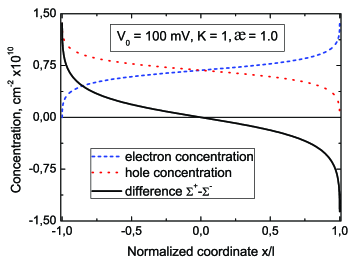
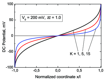
Upper panel in Fig. 2 shows examples of the spatial distributions of the electron and hole sheet concentrations in the i-section. The spatial distributions of the dc electric potential calculated for GTUNNETTs with different numbers of GLs at fixed voltage are shown in Fig. 2 (lower) panel. One can see that an increase in results in a marked concentration of the electric field near the doped sections. This is because at larger , the net tunneling generation rate becomes stronger. This, in turn, results in higher charges of propagating electron and hole components, particularly, near the p-i- and i-n-junctions, respectively.
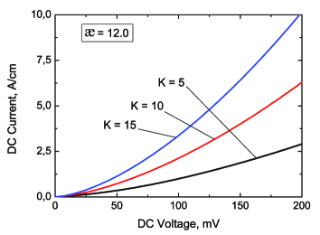
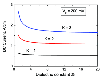
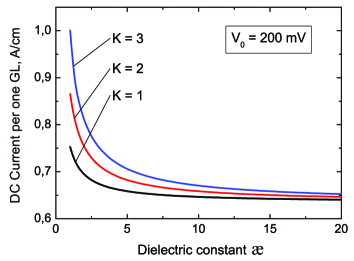
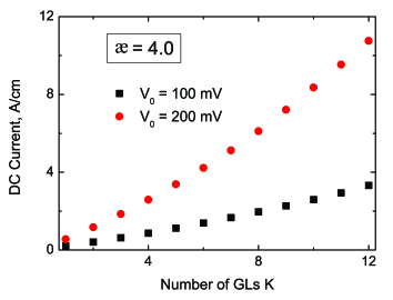
Figure 3 demonstrates a difference in the dc current-voltage characteristics in GTUNNETTs with different numbers of GLs . An increase in leads to an increase in the dc current not only because of the increase in the number of current channels but because of the reinforcement of the self-consistent electric field near the edges of the i-section(as mentioned above). As can be seen in Fig. 4 (upper panel), the three-fold increase in leads to more than three-fold increase in the dc current particularly at relatively small dielectric constants. This is confirmed by plots in Fig. 4 (lower panel), from which it follows that the dc current in each GL is larger in the devices with larger number of GLs. It is worth noting that when the dielectric constant is sufficiently large (about 15-20), the dc current in one GL is virtually the same in the devices with different number of GLs, because in this case the charge effect is suppressed. In this case the value of the dc current (per one GL) is approximately the same as that obtained in the above numerical estimate using analytical formula given by Eq. (16). In GTUNNETTs with a moderate value of , the charge effect leads to superlinear dependences of the net dc current vs number of GLs as seen in Fig. 5.
IV GTUNNETT admittance
Disregarding the term in Eq. (8) associated with the electron and hole charges in the i-section, and using Eq. (12) , one can obtain analytically the following formulas for the ac potential distribution in the i-section, and the imaginary and real parts of the GTUNNETT admittance 9 :
| (17) |
| (18) |
| (19) |
where is the dc differential conductivity, is the geometrical capacitance, is the characteristic transit time of electrons and holes across the i-section, and is the Bessel function. As follows from Eqs. (18) and (19), the admittance imaginary and real parts oscillate as functions of the transit angle with Re at near the transit time resonances , where is the resonance index.
The numerical solution of Eqs. (8), accounting for the ac components of the applied voltage and the the self-consistent charges and electric field, shows that the oscillatory frequency dependences are preserved in this more realistic case although they are be quantitatively modified. In particular, these dependences vary with varying such parameters as the number of GLs and dielectric constant . The results of numerical calculations using Eq. (8) are demonstrated in Figs. 6 - 9.
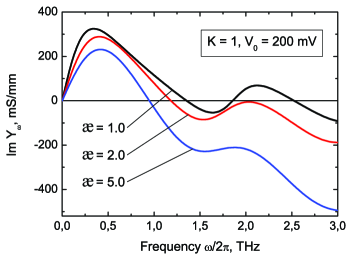
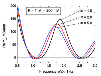
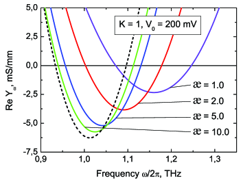
Figure 6 shows the dependence of the imaginary and real parts, Im and Re , of the admittance on the signal frequency calculated for GTUNNETTs with m and at mV at different values of dielectric constant . As follows from Fig. 6, the imaginary and real parts of the GTUNNETT admittance are oscillatory functions of the signal frequency [see also Eqs. (18) and (19)]. The oscillatory behavior is due to the transit-time resonances. At sufficiently high frequencies, the admittance imaginary part is negative because it is determined primarily by the geometrical capacitance, so that Im . In the certain frequency ranges, the admittance real part is negative as shown in Fig. 6 (lower panel). These ranges correspond to the transit-time resonances. As seen from Fig. 7 , the minima of the admittance real part (where the latter is negative) become deeper and the minima shift toward smaller frequencies with increasing dielectric constant . This is because an increase in leads to weakening of the effect of the electron and hole charges on the injection and propagation processes. The dashed line corresponds to the case when the role of these charges is diminished (very large ) considered previously 9 .
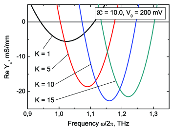
Figure 8 shows the admittance real part vs signal frequency calculated for GTUNNETTs with different number of GLs . One can see that GTUNNETTs with larger number of GLs exhibit much more deep minima (compare the curves which correspond to and in Fig. 7 and that for and in Fig. 8.). As follows from this comparison, the ten-fold increase in leads to about four-fold increase in the minimum depth.
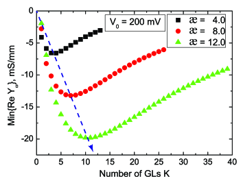
Figure 9 shows the dependence of the minimum value of the real part of the GTUNNETT admittance min on the number of GLs calculated for different dielectric constants . The nonmonotonic character of these dependences is associated with the interplay of the factors determined by the influence of electron and hole charges: an increase in leads to a suppression of these charges role, while an increase in results in proportional reinforcement of the effect of these charges accompanied by proportional increase in the current.
V Discussion
Calculating the dc current, we disregarded the contributions of the thermogeneration of electron-hole pairs in the i-section and the injection of minority carriers from the n- and p-sections.
The thermogeneration dc current is given by
| (20) |
The thermogeneration rate at the temperature K is estimated as 18 cm-2s-1. As a result, at and m from Eq. (20)one obtains A/cm.
The injection dc current can be estimated as
| (21) |
where is the Fermi energy of electrons in the n-section and holes in the p-section. Setting meV, from Eq. (21) for we find A/cm. Thus, , at least in the voltage range considered above.
The typical values of the real part of the GTUNNETT small-signal admittance in the vicinity of the first transit-time resonance () is in the range Re to mS/mm depending on and . This implies that the ac resistance, of optimized GTUNNETTs with Re mS/mm (, , and mV) and the width mm, is . Assuming that in this case A/mm at mV, the dc power, , generated by the propagating electrons and holes in the contact n- and p-regions of the device can be estimated as mW. When Re mS/mm ( and ), the same resistance is provided if mm with the dc power mW.
The depth of the minimum of the real part of the GTUNNETT admittance can be increased by applying higher bias voltage. This is because the admittance is proportional to the dc differential conductivity which, in turn, is approximately proportional to . However, an increase in results in the pertinent rise of . If exceeds the the energy of optical phonons in GLs meV, their fast emission disrupts BET and BHT in the i-section. The emission of optical phonon leads to some isotropization of the angular distribution of the electron and hole velocities of electrons and holes. This results in some decrease in their mean directed velocities (they become somewhat smaller than ) and, hence, in some increase in the electron and hole charges and the transit time. Such factors promote more steep dc current-voltage characteristics and modify the frequency dependence of the admittance. Although they should not change the GTUNNETT performance qualitatively.
The depth of the first resonance minimum of the real part of the GTUNNETT admittance with the parameters used in the above estimate is of the same order of magnitude as that of the small area (about m2) THz resonant-tunneling diodes considered by Asada et al. 19 . It is worth noting that the frequency at which Im turns zero can fall into the frequency range, where Re . In such a case, GTUNNETTs can exhibit the self-excitation of THz oscillations even without the external resonant circuit. Moreover, the contact n- and p-sections (both ungated as in the case of their chemical doping or gated in the case of the electrical ”doping”) can serve as plasma resonant cavities 9 ; 15 . The combination of the transi-time and the plasma resonances, can substantially liberalize the self-excitation conditions and enhance the THz emission efficiency. The matching of the transit-time and plasma resonant frequencies requires a proper choice of the length of the n- and p-sections (from several micrometers in the ungated structures to about one micrometer in the gated ones. The plasmons and related resonances in the gated GLs were predicted and analyzed several years ago 20 ; 21 (see also Ref. 22 . Recently, the plasmons in gated GLs were detected experimentally 23 ; 24 . It is interesting, that as a gate for the GL plasmon cavity another gate can be used 25 when the contact regions constitute double-GL structures 26 ; 27 .
VI Conclusions
We have developed a self-consistent device model for p-i-n GTUNNETTs
with different number of GLs
which enables the calculation of their realistic dc and ac characteristics.
Our calculations have shown that:
(i) The charges of electrons and holes propagating in the i-section and their effect on the spatial distribution of the self-consistent electric field
increase the steepness of the dc current-voltage characteristics. This effect is stronger in GTUNNETTs with
larger number of GLs and can be weakened by using the media surrounding GL or MGL structure (substrates and top dielectric
layers) with elevated values of the dielectric constant;
(ii) The imaginary and real parts of the GTUNNETT admittance are oscillatory
functions of the signal frequency due to the transit-time resonances.
In the certain frequency ranges, which correspond to the THz frequencies, the admittance real part can be negative
that enables the use of GTUNNETTs in the sources of THz radiation;
(iii) The charges of electrons and holes influence on the spatial distribution of the self-consistent electric field and the interband tunneling and
can substantially affect the GTUNNETT admittance, particularly, its frequency
dependence near the transit-time resonances. The role of this effect
enhances with increasing number of GLs in the device structure and can be markedly weakened in the devices with relatively large dielectric constant;
(iv) The sensitivity of the GTUNNETT characteristics to the structural parameters
(number of GLs, dielectric constant, length of the i-section) and the bias voltage
opens up wide opportunity for the optimization of GTUNNETTs for THz oscillators.
This work was partially supported by the Russian Foundation for Basic Research (grants 11-07-12072, 11-07-00505, 12-07-00710), by grants from the President of the Russian Federation (Russia), the Japan Science and Technology Agency, CREST, the Japan Society for Promotion of Science (Japan), and the TERANO-NSF grant (USA).
References
- (1) M. S. Shur and L. F. Eastman L F, IEEE Trans. Electron Devices, ED-26 1677 (1979).
- (2) M. S. Shur, IEEE Trans. Electron Devices, ED-28 1120 (1981).
- (3) V. I. Ryzhii , N. A. Bannov, and V. A. Fedirko, Sov. Phys. Semicond. 18 481 (1984).
- (4) A. K. Geim and K. S. Novoselov, Nat. Mater. 6, 183 (2007).
- (5) A. H. Castro Neto, F. Guinea, N. M. R. Peres, K. S. Novoselov, and A. K. Geim , Rev. Mod. Phys. 81 109 (2009).
- (6) M. Sprinkle, D. Suegel, Y. Hu, Hicks, J. A. Tejeda , A. Taleb-Ibrahimi, P. Le Fevre, F. Bertran, S. Vizzini, H. Enriquez, S. Chiang, P. Soukiassian, C. Berger, W. A. de Heer, A. Lanzara, and E. H. Conrad E H Phys. Rev. Lett. 103 226803 (2009).
- (7) M. Orlita and M. Potemski, Semicond. Sci. Technol. 25 063001 (2010).
- (8) V. Ryzhii , M. Ryzhii, V. Mitin, and M. S. Shur, Appl. Phys. Express, 2 034503 (2009).
- (9) V. Ryzhii, M. Ryzhii, M. S. Shur, and V. Mitin, Physica E 42 719 (2010).
- (10) V. V. Cheianov and V. I. Fal’ko , Phys. Rev. B 74 041403(R) (2006).
- (11) A. Ossipov, M. Titov, and C. V. J. Beenakker, Phys. Rev. B 75 241401(R) (2007)..
- (12) Z. S. Gribnikov, N. Z. Vagidov, V. V. Mitin, and G. I. Haddad, J. Appl. Phys. 93, 5435 (2003).)
- (13) D. Farmer, Y.-M. Lin, A. Afzali-Ardakani, and P. Avouris, Appl. Phys. Lett. 94 213106 (2009).
- (14) G. Khrenov and V. Ryzhii, IEEE Trans. Electron Devices 42, 166 (1995)
- (15) V. Ryzhii, A. Satou, I. Khmyrova, M. Ryzhii, T. Otsuji, V. Mitin, and M. S. Shur, J. Phys.: Conf. Ser. 38, 228 (2006).
- (16) W. Shocley, J. Appl. Phys. 9, 635 (1938).
- (17) S. Ramo, Proc. IRE 27, 584 (1939),
- (18) F. Rana, P. A. George, J. H. Strait, S. Shivaraman, M. Chandrashekar, and M. G. Spencer, Phys. Rev B 79, 115477 (2009).
- (19) M. Asada, S. Suzuki, and N. Kishimoto , Jpn. J. Appl. Phys. 47, 4375 (2008).
- (20) V. Ryzhii, Jpn. J. Appl. Phys. 45, L923 (2006).
- (21) V. Ryzhii, A. Satou, and T. Otsuji, J. Appl. Phys. 101 024509 (2007).
- (22) D. Svintsov, V. Vyurkov, S. O. Yurchenko, T. Otsuji, and V. Ryzhii, J. Appl. Phys. 111, 083715 (2012).
- (23) Z. Fei, A. S. Rodin, G. O. Andreev, W. Bao, et al. Nature 487, 82 (2012)
- (24) J. Chen, M. Badioli, P. Alonco-Gonzales, S. Thongrattanasari, et al. Nature 487, 77 (2012)
- (25) V, Ryzhii, T. Otsuji, M. Ryzhii, and M. S. Shur, J. Phys. D: Appl. Phys. 45, 302001 (2012).
- (26) M. Liu, X. Yin, and X. Zhang, Nano Lett. 12, 482 (2012).
- (27) L. Britnel, R. V. Gorbachev, R. Jalil, B.D . Belle, F.Shedin, A. Mishenko, T. Georgiou, M. I. Katsnelson, L. Eaves, S. V. Morozov, N. M. R. Peres, J. Leist, A. K. Geim, K. S. Novoselov, and L. A. Ponomarenko, Science, 335, 947 (2012).