Anomalous Fermi level behavior in GaMnAs at the onset of ferromagnetism
Abstract
We present the systematic study of the resonant tunneling spectroscopy on a series of ferromagnetic-semiconductor Ga1-xMnxAs with the Mn content from 0.01 to 3.2%. The Fermi level of Ga1-xMnxAs exists in the band gap in the whole region. The Fermi level is closest to the valence band (VB) at =1.0% corresponding to the onset of ferromagnetism near the metal-insulator transition (MIT), but it moves away from the VB as increases or decreases from 1.0%. This anomalous behavior of the Fermi level indicates that the ferromagnetism and MIT emerge in the Mn-derived impurity band.
The origin of the ferromagnetism and the metal-insulator transition (MIT) has been a long-debated issue in the prototype ferromagnetic semiconductor GaMnAs Matsukura et al. (1998); Jungwirth et al. (2007); Richardella et al. (2010); Chapler et al. (2011). Previously, the valence band (VB) conduction picture has been widely accepted in this material Dietl et al. (2000), where the MIT of GaMnAs was understood by the Fermi level crossing over the VB Jungwirth et al. (2007, 2010) similarly to p-type GaAs doped with non-magnetic acceptors such as Be or Zn. The ferromagnetism in GaMnAs has been thought to be induced by the VB holes interacting with the localized electrons of the Mn atoms Dietl et al. (2000); Mašek et al. (2010). However, recently, many experiments have shown the strong evidence that the Fermi level exists in the impurity band (IB) in the band gap Chapler et al. (2011); Hirakawa et al. (2002); Sapega et al. (2005, 2009); Burch et al. (2006); Ando et al. (2008); Berciu et al. (2009); Ohya et al. (2007, 2010); Ohya, Kenta, and Tanaka (2011); Rokhinson et al. (2007); Yildirim et al. (2011); Alberi et al. (2008); Mayer et al. (2010); Dobrowolska et al. (2012), which requires reconsideration on the above scenario. Therefore, to clarify the origin of the ferromagnetism and MIT in GaMnAs, it is essential to precisely investigate the Fermi level position and the VB structure of GaMnAs in the low Mn content region including the onset of ferromagnetism and MIT.
Resonant tunneling spectroscopy is a powerful method to investigate the VB structure and the Fermi level position in GaMnAs with a precision of several meV. The advantage of this method is that we can detect energy bands only with the same wave-function symmetry as that of the p-wave functions of the VB holes. Also, it is sensitive to the effective mass of the energy bands. Furthermore, by carefully analyzing the quantum-well (QW) thickness dependence of the resonant levels, we can avoid the unwanted effects induced at the surface, which prevent the precise determination of the VB or the Fermi level position Okabayashi et al. (2001); Richardella et al. (2010). Recently, from the resonant tunneling experiments in the double-barrier (DB) QW heterostructures Ohya et al. (2007, 2010) and the single-barrier structures with an ultra-thin surface GaMnAs layer Ohya, Kenta, and Tanaka (2011), it was shown that the Fermi level exists in the band gap in Ga1-xMnxAs with the Mn content higher than 5%. In this Letter, we carefully analyze the VB structure and the Fermi level position in a series of Ga1-xMnxAs from the unexplored insulating region (=0.01%) to the metallic region (=3.2%). We find that the VB structure is not largely affected by the Mn doping and that the Fermi level never crosses over the VB near the MIT: The Fermi level becomes closest to the VB at =1.0% at the onset of the ferromagnetism, but it moves away from the VB as increases or decreases from 1.0%. This anomalous behavior of the Fermi level is completely different from that of GaAs doped with other shallow acceptors.

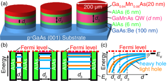
Figure 1(a) shows the schematic device structures investigated in this study. We grew DB-QW heterostructures composed of (from the top to the bottom) Ga0.94Mn0.06As (20 nm) / AlAs (6 nm) / Ga1-xMnxAs QW ( nm) / AlAs (6 nm) / GaAs:Be (100 nm, Be concentration: 118 cm-3) by low-temperature molecular-beam epitaxy (MBE). Table 1 shows the characteristics of the GaMnAs QW samples examined in this study. The Mn content of sample D-H, F2, and G2 was determined by the x-ray diffraction measurements for the 100 nm-thick reference GaMnAs samples grown in the same condition as that for the GaMnAs QW in each DB-QW sample. We estimated of sample A-C and C2 from an Arrhenius plot of the Mn flux vs. the K-cell temperature obtained from the flux data of sample D-H, F2, and G2. In this study, was varied from 0.01% to 3.2%. In this Mn content range, as increases, GaMnAs changes from insulating paramagnetic to insulating ferromagnetic at =1%. At 2%, it starts to show the metallic behavior, in which the resistivity decreases as temperature decreases at (Curie temperature). The values of the Ga1-xMnxAs QW in sample D-H, F2, and G2 were obtained from the temperature dependence of tunneling magnetoresistance (TMR) observed in these devices. As shown in Table 1, the Ga1-xMnxAs QW with =1-3% has lower than that of the surface Ga0.94Mn0.06As (60-70 K) due to the low in the QWs. To obtain the resonant tunneling diodes with various GaMnAs QW thickness on a same wafer, we linearly moved a shutter in front of the substrate while growing the Ga1-xMnxAs QW, in which was varied from 10 nm to 16 nm within the wafer of mm2 Tanaka and Higo (2001). Also, we prepared sample C2 (=0.3%), F2 (=1.6%), and G2 (=2.3%) with from 4 nm to 10 nm, where the growth conditions of sample C2, F2, and G2 are the same as those of sample C (=0.3%), F (=1.6%), and G (=2.3%) except for , respectively. The values of were estimated from the speed of the shutter. Although simple structures (GaMnAs / AlAs / GaAs:Be single-barrier heterostructures) were used in Ref. Ohya, Kenta, and Tanaka, 2011, they are not applicable for this study due to the low Mn contents 2% in the GaMnAs QW that we are using here. The low Mn contents in the surface GaMnAs induce a large depletion thickness at the surface, making an electrical contact to the GaMnAs layer very difficult. Thus, the DB-QW structures are the best structure for our current purpose. The details about the preparation of the samples are described in the supplemental material sup .
| Sample. | (%) | (∘C) | (nm) | (K) | (meV) |
|---|---|---|---|---|---|
| Sample A | 0.01 | 400 | 10 - 16 | paramagnetic | 60 |
| Sample B | 0.1 | 350 | 10 - 16 | paramagnetic | 35 |
| Sample C | 0.3 | 330 | 10 - 16 | paramagnetic | 25 |
| Sample C2 | 0.3 | 330 | 4 - 10 | paramagnetic | 25 |
| Sample D | 1.0 | 265 | 10 - 16 | 25 | 4 |
| Sample E | 1.2 | 260 | 10 - 16 | 30 | 6 |
| Sample F | 1.6 | 250 | 10 - 16 | 40 | 10 |
| Sample F2 | 1.6 | 250 | 4 - 10 | 25 | 7 |
| Sample G | 2.3 | 240 | 10 - 16 | 45 | 17 |
| Sample G2 | 2.3 | 240 | 4 - 10 | 30 | 12 |
| Sample H | 3.2 | 230 | 10 - 16 | 60 | 25 |
Figure 1(b) shows the schematic VB profiles of the DB-QW devices shown in Fig. 1(a). The black solid and red dash-dotted lines indicate the VB top and Fermi level, respectively. The blue and orange lines are the resonant levels of the heavy hole (HH) and light hole (LH), respectively. Here, the small exchange splitting is neglected for simplicity. Figure 1(c) shows the schematic dependence of the resonant levels. The resonant levels converge on the VB top energy of the bulk GaMnAs as increases. Since the Fermi level corresponds to the zero bias condition, the Fermi level position can be determined by measuring bias voltage corresponding to in sufficiently wide . The bias polarity is defined by the voltage of the top GaMnAs electrode with respect to the substrate.
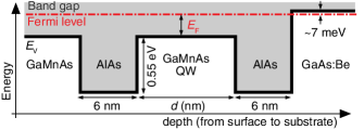
Figure 2 shows the VB diagram of the investigated DB-QW devices assumed in the following theoretical calculation of the resonant levels. The black solid and red dash-dotted lines are and the Fermi level, respectively. The gray region is the band gap. For the quantum level calculation, we used the Luttinger-Kohn Hamiltonian Wessel and Altarelli (1989) and transfer matrix method Tsu and Esaki (1973). The VB offset between AlAs and GaMnAs was assumed to be 0.55 eV. We assumed that the in-plain wave vector is during the tunneling, because holes are injected from the GaAs:Be electrode in the negative bias region and holes in the GaAs:Be electrode exist only around the point. For simplicity, the small band bending was neglected sup .


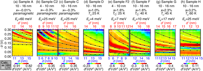
Figure 3(a)-(h) show the color contour maps of the - as a function of in sample A, C2, C, D, F2, F, G, and H measured at 3.5 K in the negative bias region, respectively. Here, the color-coded intensities are extrapolated from the measured data at the values corresponding to the white dots shown at the top of these figures. The black square and white triangle dots are calculated resonant peak bias voltages of the HH and LH bands, respectively. is the energy distance between and the Fermi level. Clear oscillations due to the resonant tunneling are observed in all the - curves. Moreover, the resonant peak bias voltages become smaller as increases, which is well reproduced by the calculated dependence of the resonant peak bias voltages. The value is estimated by the following procedure. As increases to infinity, these resonant levels converge on a certain voltage corresponding to the valence band edge. The Fermi level position corresponds to the zero bias. Experimentally, the measured voltage is proportional to the energy (relative to the Fermi level); =. Therefore, corresponds to the energy distance between the Fermi level and . Then, the dependence of is calculated from the equation = in individual . Here, is quantum level energy with respect to the Fermi level. In the fitting, we slightly shifted the value to in order to obtain the perfect fit. The value of used in the calculation was shown as the upper red ruler of the contour maps. The necessity of this shift of is due to the difficulty in accurately controlling the relative positions between the substrate shutter and the sample wafer inside the MBE chamber. We note that, however, the thickness difference between and is only less than 3 nm. The value corresponds to the ratio of the total bias voltage to the voltage applied at the bottom AlAs barrier. The values are assumed to be 2.0 in this study. Considering that is 2 in ideal DB tunnel junctions Tsu and Esaki (1973) and that the interstitial Mn and its distribution variation in the QW are sufficiently suppressed in the low with the relatively high growth temperature, the =2.0 assumed in this study is sufficiently reasonable. The color contour maps of the in all the samples are shown in the supplemental material sup .
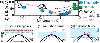
In Fig. 4, the blue circles are the values obtained in this study. The green squares are the ones reported in Ref. Ohya, Kenta, and Tanaka, 2011. The black pentagons are the thermal-activation energy of the Mn acceptors in GaAs obtained by the magneto-transport measurements in Ref. Blakemore et al., 1973. The pink curve is the calculated values obtained from the equation mentioned in Ref. Blakemore et al., 1973. Here, we selected 0.8% as the intercept of to fit the curve to the experimental data. The gray dash-dotted, dashed, and solid curves are the calculated by the valence-band anti-crossing model (VBAC) Alberi et al. (2007) and the free-electron approximation. In the VBAC, the impurity level are assumed to be 0.1, 0.05, and 0.01 eV, respectively. Also, the anti-crossing coupling constant is assumed to be 0.18 eV. The free-electron approximation calculation for the Fermi level position in the IB is done by roughly assuming the hole concentration to be /2 and the effective mass to be Burch et al. (2006), where is the electron mass. Figure 4(b)-(d) show the VB and IB diagrams expected from this study in the (b) insulating paramagnetic (), (c) insulating ferromagnetic (=1-2%), and (d) metallic ferromagnetic () regions, respectively. The black solid curves correspond to the VB. The blue dotted lines correspond to the upper and bottom edges of the IB. The blue region represents the IB region. The red dash-dotted lines correspond to the Fermi level. In the paramagnetic GaMnAs (), decreases as increases, which is quantitatively consistent with the activation-energy-lowering effect observed in the magneto-transport measurements Blakemore et al. (1973). This behavior is the same as the one in the insulating region of the non-magnetic accepter-doped -type GaAs Hill (1970). The Fermi level behavior in the paramagnetic region is caused by the screening effect due to the heavy Mn doping, which makes the IB position close to the VB. On the other hand, increases as increases in the ferromagnetic GaMnAs with , which means that the Fermi level moves away from the VB. This behavior is qualitatively explained by the VBAC model [the gray solid curve in Fig. 4(a)]. The quantitative discrepancy between the experimental and calculated Fermi level is probably because is probably because this calculation does not take into account the screening and many body effects. This Fermi level behavior in the ferromagnetic region means that the IB truly exists in the ferromagnetic GaMnAs and the anti-crossing interaction is induced by the electron-electron interaction Alberi et al. (2008).

Figure 4(a) shows that the Fermi level exists in the IB in the band gap in whole the region, which suggests that the ferromagnetism is strongly related to the IB. At the MIT border (=2%), the Fermi level is still in the band gap, which suggests that the MIT occurs in the IB. This behavior of the Fermi level is completely different from that in the case of the heavily-doped -type GaAs with the non-magnetic acceptors and contradicts the VB conduction picture, where the IB completely merges into the VB. The IB still exists in the metallic GaMnAs, which means that the impurity states still remain in the band gap. This is probably because the holes are trapped into the acceptor states induced by - hybridized orbitals after the Coulomb potential completely screened Mahadevan and Zunger (2004); Tang and Flatté (2004). At the onset of the ferromagnetism (=1%), the dependence of the Fermi level changes, which is thought to be induced by the change of the main effect for determining the IB position from the screening effect to the anti-crossing interaction. This must give a clue to understanding the mechanism of the ferromagnetism. We note that this anomalous behavior of the Fermi level is not directly related to the MIT because the MIT and the turning up of the Fermi level position occur at slightly different value of (1.5 - 2% and 1%, respectively).
In summary, we fabricated the DB heterostructures containing a Ga1-xMnxAs QW with various . From the resonant tunneling measurements in these structures, we found that the Fermi level exists in IB in the band gap in the whole range of . When is less than 1.0%, the Fermi level becomes close to the VB top as increases, which is induced by the screening effect. At =1.0% around the emergence of the ferromagnetism, the Fermi level becomes closest to the VB, where is 4 meV. When is larger than 1.0%, the Fermi level goes further away from the VB top as increases, which is qualitatively explained by the anti-crossing interaction. The anomalous behavior of the Fermi level means that the ferromagnetic GaMnAs is completely different from the non-magnetic heavily-doped -type GaAs, which indicates that the IB in the ferromagnetic GaMnAs is composed of the - hybridized orbitals. Our results clearly show that the ferromagnetism and the MIT are strongly related to the formation of the Mn-derived IB.
Acknowledgements.
This work was partly supported by Grant-in-Aids for Scientific Research including Specially Promoted Research, the Special Coordination Programs for Promoting Science and Technology, and FIRST Program of JSPS.References
- Matsukura et al. (1998) F. Matsukura, H. Ohno, A. Shen, and Y. Sugawara, Phys. Rev. B 57, R2037 (1998).
- Jungwirth et al. (2007) T. Jungwirth, J. Sinova, A. H. MacDonald, B. L. Gallagher, V. Novák, K. W. Edmonds, A. W. Rushforth, R. P. Campion, C. T. Foxon, L. Eaves, E. Olejník, J. Mašek, S.-R. E. Yang, J. Wunderlich, C. Gould, L. W. Molenkamp, T. Dietl, and H. Ohno, Phys. Rev. B 76, 125206 (2007).
- Richardella et al. (2010) A. Richardella, P. Roushan, S. Mack, B. Zhou, D. A. Huse, D. D. Awschalom, and A. Yazdani, Science 327, 665 (2010).
- Chapler et al. (2011) B. C. Chapler, R. C. Myers, S. Mack, A. Frenzel, B. C. Pursley, K. S. Burch, E. J. Singley, A. M. Dattelbaum, N. Samarth, D. D. Awschalom, and D. N. Basov, Phys. Rev. B 84, 081203 (2011).
- Dietl et al. (2000) T. Dietl, H. Ohno, F. Matsukura, J. Cibert, and D. Ferrand, Science 287, 1019 (2000).
- Jungwirth et al. (2010) T. Jungwirth, P. Horodyská, N. Tesařová, P. Němec, J. Šubrt, P. Malý, P. Kužel, C. Kadlec, J. Mašek, I. Němec, M. Orlita, V. Novák, K. Olejník, Z. Šobáň, P. Vašek, P. Svoboda, and J. Sinova, Phys. Rev. Lett. 105, 227201 (2010).
- Mašek et al. (2010) J. Mašek, F. Máca, J. Kudrnovský, O. Makarovsky, L. Eaves, R. P. Campion, K. W. Edmonds, A. W. Rushforth, C. T. Foxon, B. L. Gallagher, V. Novák, J. Sinova, and T. Jungwirth, Phys. Rev. Lett. 105, 227202 (2010).
- Hirakawa et al. (2002) K. Hirakawa, S. Katsumoto, T. Hayashi, Y. Hashimoto, and Y. Iye, Phys. Rev. B 65, 193312 (2002).
- Sapega et al. (2005) V. F. Sapega, M. Moreno, M. Ramsteiner, L. Däweritz, and K. H. Ploog, Phys. Rev. Lett. 94, 137401 (2005).
- Sapega et al. (2009) V. F. Sapega, N. I. Sablina, I. E. Panaiotti, N. S. Averkiev, and K. H. Ploog, Phys. Rev. B 80, 041202 (2009).
- Burch et al. (2006) K. S. Burch, D. B. Shrekenhamer, E. J. Singley, J. Stephens, B. L. Sheu, R. K. Kawakami, P. Schiffer, N. Samarth, D. D. Awschalom, and D. N. Basov, Phys. Rev. Lett. 97, 087208 (2006).
- Ando et al. (2008) K. Ando, H. Saito, K. C. Agarwal, M. C. Debnath, and V. Zayets, Phys. Rev. Lett. 100, 067204 (2008).
- Berciu et al. (2009) M. Berciu, R. Chakarvorty, Y. Y. Zhou, M. T. Alam, K. Traudt, R. Jakiela, A. Barcz, T. Wojtowicz, X. Liu, J. K. Furdyna, and M. Dobrowolska, Phys. Rev. Lett. 102, 247202 (2009).
- Ohya et al. (2007) S. Ohya, P. Nam Hai, Y. Mizuno, and M. Tanaka, Phys. Rev. B 75, 155328 (2007).
- Ohya et al. (2010) S. Ohya, I. Muneta, P. N. Hai, and M. Tanaka, Phys. Rev. Lett. 104, 167204 (2010).
- Ohya, Kenta, and Tanaka (2011) S. Ohya, T. Kenta, and M. Tanaka, Nature Physics 7, 342 (2011).
- Rokhinson et al. (2007) L. P. Rokhinson, Y. Lyanda-Geller, Z. Ge, S. Shen, X. Liu, M. Dobrowolska, and J. K. Furdyna, Phys. Rev. B 76, 161201 (2007).
- Yildirim et al. (2011) M. Yildirim, S. March, R. Mathew, A. Gamouras, X. Liu, M. Dobrowolska, J. K. Furdyna, and K. C. Hall, Phys. Rev. B 84, 121202 (2011).
- Alberi et al. (2008) K. Alberi, K. M. Yu, P. R. Stone, O. D. Dubon, W. Walukiewicz, T. Wojtowicz, X. Liu, and J. K. Furdyna, Phys. Rev. B 78, 075201 (2008).
- Mayer et al. (2010) M. A. Mayer, P. R. Stone, N. Miller, H. M. Smith, O. D. Dubon, E. E. Haller, K. M. Yu, W. Walukiewicz, X. Liu, and J. K. Furdyna, Phys. Rev. B 81, 045205 (2010).
- Dobrowolska et al. (2012) M. Dobrowolska, K. Tivakornsasithorn, X. Liu, J. K. Furdyna, M. Berciu, K. M. Yu, and W. Walukiewicz, Nat. Mater. 11, 444 (2012).
- Okabayashi et al. (2001) J. Okabayashi, A. Kimura, O. Rader, T. Mizokawa, A. Fujimori, T. Hayashi, and M. Tanaka, Phys. Rev. B 64, 125304 (2001).
- Tanaka and Higo (2001) M. Tanaka and Y. Higo, Phys. Rev. Lett. 87, 026602 (2001).
- (24) See Supplemental Material for the details about the sample preparation, the results in all the samples, and other discussion.
- Wessel and Altarelli (1989) R. Wessel and M. Altarelli, Phys. Rev. B 39, 12802 (1989).
- Tsu and Esaki (1973) R. Tsu and L. Esaki, Appl. Phys. Lett. 22, 562 (1973).
- Blakemore et al. (1973) J. S. Blakemore, J. Winfield J. Brown, M. L. Stass, and D. A. Woodbury, J. Appl. Phys. 44, 3352 (1973).
- Alberi et al. (2007) K. Alberi, J. Wu, W. Walukiewicz, K. M. Yu, O. D. Dubon, S. P. Watkins, C. X. Wang, X. Liu, Y.-J. Cho, and J. Furdyna, Phys. Rev. B 75, 045203 (2007).
- Hill (1970) D. E. Hill, J. Appl. Phys. 41, 1815 (1970).
- Mahadevan and Zunger (2004) P. Mahadevan and A. Zunger, Appl. Phys. Lett. 85, 2860 (2004).
- Tang and Flatté (2004) J.-M. Tang and M. E. Flatté, Phys. Rev. Lett. 92, 047201 (2004).