Far-field emission profiles from L3 photonic crystal cavity modes
Abstract
We experimentally characterize the spatial far-field emission profiles for the two lowest confined modes of a photonic crystal cavity of the L3 type, finding a good agreement with FDTD simulations. We then link the far-field profiles to relevant features of the cavity mode near-fields, using a simple Fabry-Perot resonator model. The effect of disorder on far-field cavity profiles is clarified through comparison between experiments and simulations. These results can be useful for emission engineering from active centers embedded in the cavity.
I Introduction
Photonic crystals (PhC) offer unprecedented control over electromagnetic field confinement in all three spatial directions Joannopoulos et al. (2008). In particular, two-dimensional PhC nanocavities in a planar waveguide have already found applications in different fields such as nanolasers, nonlinear optics and quantum information processing Yao et al. (2010); O’Brien et al. (2009). Similar to any electromagnetic resonator, PhC nanocavity modes are essentially characterized by two figures of merit: the cavity quality factor, , and the effective confinement volume of each mode, Notomi (2010). The quality factor is proportional to the photon lifetime in the cavity which depends on the cavity losses to the external world. The mode volume is a quantitative measure of the spatial confinement of the electromagnetic mode. In most applications, it is crucial to maximize the ratio. For example, the Purcell factor, which measures the enhancement of the spontaneous emission rates for atoms resonant with a cavity is directly proportional to this figure of merit. In PhC nanocavities the mode is strongly confined to a very small volume, on the order of , where is the mode wavelength. In a planar membrane nanocavity, in-plane confinement is provided by spatial localization of a structural defect in a perfectly periodic PhC with a photonic band-gap, while out-of-plane confinement is given by total internal reflection between the slab and the air cladding (assuming a suspended membrane as a planar waveguide). Very high quality factors, in the range - Akahane et al. (2003); Song et al. (2005); Kuramochi et al. (2006) have been demonstrated in the literature. In particular, the L3-type cavity, consisting of three missing holes in a triangular lattice, was the first PhC cavity to show quality factors larger than Akahane et al. (2003).
The spectral mode structure for L3 cavities has been thoroughly investigated by Chalcraft and coworkers Chalcraft et al. (2007) who compared the calculated resonant energies, quality factors and emission polarizations for the lowest-order modes with experimental data. Most experiments coupling single quantum dot emitters to a nanocavity exploit the fundamental (i.e. lowest-energy) cavity mode Strauf et al. (2006); Hennessy et al. (2007). However, higher order modes can still be important for, e.g., efficient pumping in nanocavity lasers Nomura et al. (2006a), selective excitation of quantum dots embedded within the cavity Nomura et al. (2006b); Oulton et al. (2007), or mutually coupling quantum dots in different spatial positions Imamoglu et al. (2007). Several groups have studied the near-field emission profiles of photonic crystal nanocavities Mujumdar et al. (2007); Intonti et al. (2008), even with polarization-resolving imaging Vignolini et al. (2009).
In this paper we report an experimental and theoretical investigation of the spatial far-field profile of the out-of-plane emission for the two lowest-order modes of L3-type PhC nanocavities. We believe the characterization of the out-of-plane far-field emission for PhCs is important for two main reasons. First, for single-photon source applications the emitted radiation needs to be efficiently collected into a fiber, and simultaneous optimization of far-field emission for multiple nanocavity resonances could be useful. In addition, in the case of cavity-QED experiments in the “one-dimensional atom” approximation, a perfect mode-matching is needed to get a large enough interference between the input light field and the field radiated by the atom Waks and Vuckovic (2006); Aufféves-Garnier et al. (2007); Bonato et al. (2010). Recently, quite some work has been done to get a beam-like vertical emission from PhC nanocavities Kim et al. (2006); Tran et al. (2009); Toishi et al. (2009); Portalupi et al. (2010) for the fundamental mode. Here we extend previous work by experimentally analyzing the far-field emission properties of both the fundamental and the second-order mode, finding good agreement with numerical simulations. We introduce a simple model, based on a one-dimensional Fabry-Perot resonator, to estimate the essential far-field characteristics of a given near-field mode profile and link them to the relevant device parameters. We believe that such a model can be useful for fast parameter optimization, while full-scale numerical simulations can provide an accurate but time-consuming description of the electromagnetic field in the structure. Finally, we will discuss the effect of fabrication imperfections on the far-field cavity emission profiles. As we will show, measurements of far-field profiles are relatively easy to perform and they can provide insightful information about the parameters and the quality of the cavities under examination.
The paper is organized as follows: in Section II, we present experimental measurements of the far-field profiles and a comparison with theoretical far-fields extracted from finite-difference-time-domain (FDTD) simulations; in Section III, we introduce a simple model, based on a Fabry-Perot resonator, which is sufficient to give indications of what the actual far-field profile looks like for a given near-field and to link far-field properties to actual device parameters.
II Theoretical modeling and experimental data
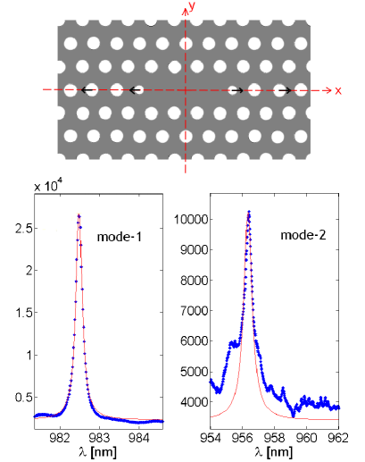
Our sample consists of a nm GaAs membrane grown by molecular beam epitaxy on top of a 0.92 m Al0.7Ga0.3As sacrificial layer on a GaAs substrate. An In0.4Ga0.6As quantum dot layer is grown at the center of the GaAs membrane by depositing periods of Å-thick InAs and Å-thick In0.13Ga0.87As. The L3 PhC cavities were fabricated on the sample using standard electron beam lithography and reactive ion etching techniques Badolato et al. (2005); Thon et al. (2009). The lattice constant of the triangular hole lattice is nm. The L3 cavity design was properly modified for optimization (see modified holes in Fig. 1) Andreani et al. (2004); Akahane et al. (2005).
The sample was placed in a He-flow cryostat at about K and illuminated above the GaAs bandgap with a few mW laser beam (wavelength nm) on a few m2 spot. The photoluminescence from the quantum dot layer embedded in the membrane was collected in the direction normal to the membrane using a microscope objective with numerical aperture and spectrally analyzed with a spectrometer (resolution GHz/pixel). An example of the spectral emission is shown in Fig. 1 for a device with nm. According to theoretical predictions based on a guided-mode expansion method Andreani and Gerace (2006), the cavity supports two confined modes, with resonances respectively at nm (theoretical Q-factor ) and nm (). Experimentally, we measured the first-order mode with a Lorentzian profile centered around = nm with a full-width at half-maximum (FWHM) of nm, from which we extract an experimental quality factor of . On the other hand, the second-order mode has a less perfect Lorentzian lineshape centered around = nm with FWHM nm, and an experimental Q-factor . Experimental quality factors are lower then the predicted ones due to scattering from fabrication imperfections Portalupi et al. (2011) and possible absorption from sub-bandgap trap levels and surface states Michael et al. (2007).
Experimentally, the emitted radiation collected from both modes results in a strongly linearly polarized signal.
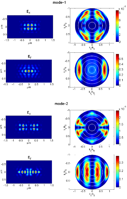
However, as it is shown in the 3D FDTD simulations of Fig. 2, each near-field mode profile has x- and y-components of the electric
field of comparable intensity. The reason for the detection of linearly polarized light can be found by calculating the far-field projections of such
polarization-resolved near-field profiles.
The far-field profile can be obtained from the near-field using the procedure introduced by Vuckovic and coworkers Vuckovic et al. (2002).
According to the surface equivalence theorem, all the information about the far-field profile can be obtained from equivalent electric and magnetic
currents, and ,
which depend on the in-plane near field components:
| (1) |
where denoted the two-dimensional Fourier transform. These equivalent currents are used to calculate the retarded vector potential of the electromagnetic field, which in the far-field can be related to Fourier transforms of the near-fields. The radiation intensity per unit solid angle can be calculated as:
| (2) |
where is the impedance of free-space and is the mode wavelength. The radiation vectors in spherical coordinates can be expressed from their cartesian components as:
| (3) |
and similarly for . The far-field profiles calculated from the near-fields in the left panels of Fig. 2 are shown in the same figure, on the right. In these plots, the color scale is normalized to the totally emitted power in the upper half-space of the PhC cavity (the same normalization factor is used for and ). Most of the emission from the x-polarization of both modes is predicted at very large angles,and therefore is inefficiently collected by commonly employed microscope objectives. This results in the strong linear polarization observed in the photoluminescence spectra.
To perform a direct measurement of the far-field emitted intensity at each resonant mode frequency, the filtered photoluminescence at the back focal plane of the microscope objective is imaged. Given a characteristic size of the near-field emission, 500 nm, at a wavelength m the Fresnel number is , well in the far-field regime ( mm). The far-field was imaged on an intensified CCD camera by a lens with focal length cm in a configuration. To make sure that we were looking at the microscope objective back focal plane, we adjusted the lens to see the sharp image of the objective edge on the CCD. This sharp edge was used to calibrate the numerical aperture scale of the far-field images, assuming that the sharp edges correspond to the of the objective employed. An interference filter, with a bandwidth nm, was used to spectrally select the mode of interest. Images were collected after integrating for s and the background noise was removed by subtracting an image taken with a slightly tilted interference filter.
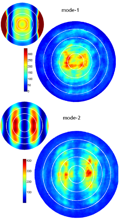
The experimental far-field spatial emission profiles for the first-order and second-order modes are shown in the two larger plots on the right side of
Fig. 3, together with the far-field projections obtained from FDTD simulations (smaller insets on the left) for a direct comparison.
The first-order mode exhibits a centrally illuminated area extending to about , with a ring-like structure inside (),
matching the low-NA portion of the simulated far-field. The simulated far-field suggests that most of the light from the first-order mode is emitted in two high-NA lobes, which are not collected at all by our set-up.
The far-field profile for the second-order mode consists of two lobes, whose center is at a minimal .
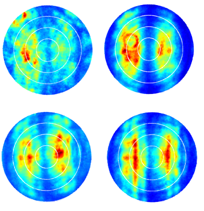
Finer details also appear inside the two lobes, in the form of spots separated by . Such structures correspond, in the near-field, to light sources which are separated from the cavity about times the characteristic size of the cavity mode. The simulated near-field profiles shown in Fig. 2 suggest that the optical field decays very fast out of the cavity region, implying that such features might be due to light that escapes from the cavity due to fabrication imperfections Portalupi et al. (2011). The fine details are reproducible for different measurements performed on the same device. Finally, we show in Fig. 4 the far-field profiles of the second-order modes for different devices on the same wafer. Each plot shows the characteristic two-lobes profile, as expected for this mode, with reproducible finer details that appear to be device-dependent.
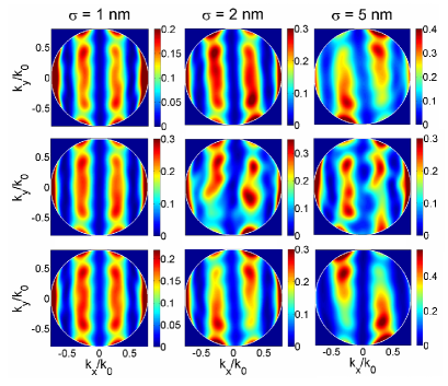
To investigate the cause of fine structure within the two-lobe far-field pattern of the second order mode, FDTD simulations were done in which disorder was introduced. It is assumed that, due to fabrication imperfections, the dominant type of disorder is in the hole radii of the PhC lattice. Therefore, the hole radii were varied randomly according to the distribution function . Some simulation data are given in Figure 5, showing disorder introduced to the far-field profiles as a result of increasing the disorder parameter . These results indicate that far-field measurements could be used as an indicator of disorder in the lattice structure.
III A simple Fabry-Perot model
In general, 3D FDTD simulations can provide accurate modeling of near-field and far-field properties of PhC cavity modes. However, they give little physical insight on how the detected features of such far-field profiles can be related to specific device parameters. In this Section, we will show that the experimental data can be reproduced by a simple model, elaborated from the proposal of Sauvan and coworkers Sauvan et al. (2005).
For a line of missing holes, the PhC nanocavity can be described quite accurately by a Fabry-Perot resonator, in which the fundamental Bloch mode of a single-line-defect PhC waveguide is trapped between two PhC mirrors of modal reflectivity . The properties of such a cavity are shown to depend only on three parameters, namely the group index of the Bloch mode, the reflection coefficient of the mirrors and the effective cavity length . The Bloch mode can be calculated as the eigenstate of the PhC waveguide in the Fourier basis, and its modal reflectivity can be obtained with the method described in Ref. Silberstein et al. (2001). Fabry-Perot models have been shown to be a useful tool to probe cavity resonances and the group index of photonic crystal waveguides Combrié et al. (2006); Lalanne et al. (2008), and to describe acousto-mechanical cavity tuning effects Fuhrmann et al. (2011). We consider the near-field profiles shown in Fig. 2. Taking the intensity distribution along the axis, the modes show a sinusoidal intensity distribution with nodes and antinodes in the cavity region, decaying exponentially outside the cavity region. From simulations, the intensity decay length for the first-order mode is nm, while it is nm for the second-order mode. This is very similar to the intensity distribution in a cavity between two Distributed Bragg Reflectors (DBR). For the near-field profiles most of the radiation is emitted along the axis, with little structure and weaker intensity outside. Given the relevance of such polarization in determining the far-field emission properties, to a first-order approximation it makes sense to consider a one-dimensional model, which takes into account only the structure along the axis. Such a model has the advantage of being extremely simple, although able to give significant hints on the main far-field profile properties. A two-dimensional model based on an effective index approximation should be used (with no significant difficulties) to study also the profiles.
Let us consider a one-dimensional Fabry-Perot resonator, with the field intensity profile varying sinusoidally in the cavity region and exponentially decaying in the mirror regions, with characteristic penetration depth . The resonant frequency can be calculated by imposing the total phase acquired by the Bloch mode traveling back and forth to be a multiple of . The far-field profile can be calculated using the procedure outlined in the previous Section (Eq. 2). Since the modes are TE-like modes, only , and are non-negligible and only the component is relevant in Eq. 2. Let’s consider a separable electric field distribution . The component is separable as well: , where and are the one-dimensional Fourier transforms of and , making:
| (4) |
In a simplified one-dimensional model, is narrow in real-space, so its Fourier transform is wide and can be neglected (). If we look at the far-field distribution along the x-axis we select , so that the resulting one-dimensional far-field profile is:
| (5) |
or, in terms of transverse wavevectors: .
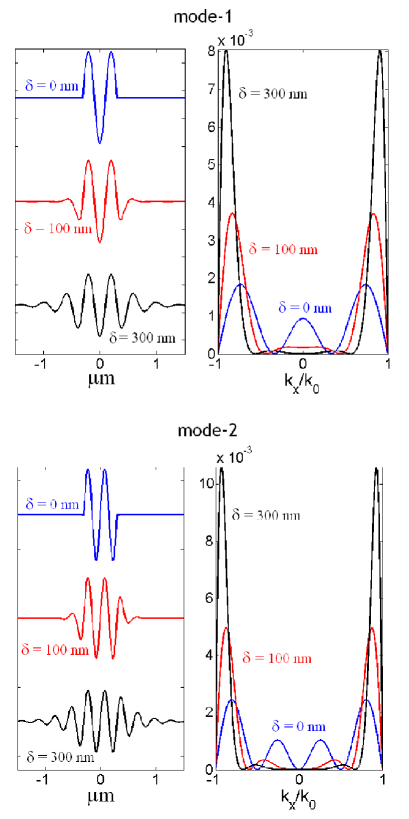
An analytical solution can be found and is reported in Appendix A. However, the resulting formula is too complicated to give intuitive insights; therefore we will just discuss the numerical results (from Eq. 12) in this context. Fig. 6 shows the expected far-field profiles for the first and second-order modes for different values of the penetration depth, . The first-order mode exhibits a central peak (centered at ) and two outer lobes as predicted by the FDTD simulations. We see that, for increasing penetration depth, the two main outer lobes become narrower in k-space and more outward, while the central peak broadens and flattens. A similar behavior can be observed in the second-order mode. Here, the far-field profile is given by two central peaks and two outer lobes, and again, for increasing penetration depth the two outer lobes move outwards and become more localized.
The Fabry-Perot resonator model was shown to give results for the quality factor in agreement with more sophisticated FDTD simulations Sauvan et al. (2005):
| (6) |
where the group delay experienced by the light upon mirror reflection enters as a characteristic length . In general, for PhC structures (for example, heterostructure mirrors) it has been shown that can be unrelated to the characteristic damping length of the energy distribution inside the mirrors Sauvan et al. (2009). However, in the configuration under investigation, the classical relation for a DBR, , is valid, with the equality being strictly fulfilled only in the limiting case of quarter-wave mirrors with low refractive index contrast, ().
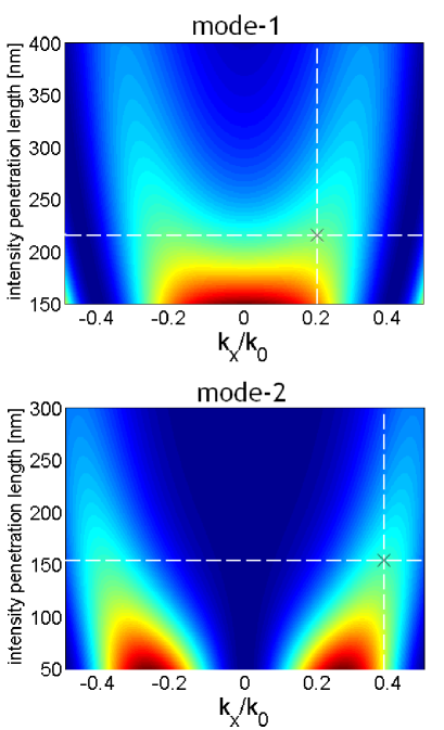
In Fig. 7, the emission in the region is shown as a function of the penetration depth. In the case of the fundamental mode, there is a single peak centered around for small penetration depth, with a quite flat profile and broadening for . When the penetration depth increases beyond nm, the far-field emission splits into two lobes, which separate more and more on increasing . At nm, the peaks are centered around , corresponding to an opening angle of about degrees. These findings explain the ring-like structure we observe in the experimental far-field: the vertical dashed white line in the figure shows the experimental central NA for the peaks (from Fig. 3), which corresponds to a penetration depth of about nm, fully compatible with the penetration depth from FDTD simulations, . For the second-order mode, in the region there are always two emission lobes, even at small penetration depth. On increasing , the two lobes move further and further apart. From Fig. 3, the lobes are centered around , which in our simulations is consistent with a penetration depth of about nm, as predicted by FDTD simulations. Therefore, far-field profiles can provide useful information about the penetration depth of PhC cavity modes, which in this case offer a bound on the effective cavity length, , and therefore on the Q-factor. Extensions of the present analysis to treat coupled cavity modes Intonti et al. (2011); Brunstein et al. (2011) can also be considered.
IV Conclusions
In conclusion, we have presented an extensive characterization of far-field emission profiles from L3-type photonic crystal nanocavities,
introducing a simple imaging technique as an efficient tool to give a two-dimensional mapping of the emitted intensity.
The measurements have been directly compared to theoretically modeled far-field projections from the 3D FDTD near-field
cavity modes profiles, and we believe these results to be useful to PhC cavity designs for specific purposes. The effect of disorder on the far-field profiles was investigated via numerical simulations.
Finally,we have introduced a simple Fabry-Perot model that is able to capture the essential features of far-field properties
for suitably designed near-field profiles. As a particular application of this model, we can envision, for example, the simultaneous optimization of in- and out-coupling for two different
modes supported by the same PhC cavity, which is still an open problem that might benefit from simplified models like the one presented here.
Acknowledgments
The authors acknowledge helpful discussions with Morten Bakker. This work was supported by NSF NIRT Grant No. 0304678, Marie Curie EXT-CT-2006-042580 and FOMNWO grant No. 09PR2721-2. A portion of this work was done in the UCSB nanofabrication facility, part of the NSF funded NNIN network.
Appendix A: Analytical calculations
The resonance frequencies for the modes can be found by setting the condition that the total phase acquired by the Bloch mode traveling back and forth is a multiple of (), which results in:
| (7) |
Let us start with a perfectly confined mode, with no penetration into the mirrors (). In this case the field is given by:
| (8) |
where is the rectangular function, for and zero elsewhere. The phase is set by the boundary conditions: for even (cosine-like solutions) and for odd (sine-like solutions). From Eq. 4:
| (9) |
The two modulo-squared Sinc functions in Eq. 9 give two main peaks centered at , which correspond to the higher-NA peaks in the far-field in Fig. 6. The first relative maximum of is at , which for Eq. 9 corresponds to . The FWHM of such a peak for is , which corresponds to ( for the first-order mode, corresponding to , and for the second-order mode, corresponding to ). Therefore for the first-order mode, the first relative maxima of the Sinc functions superpose, giving just one central peak. For the secod-order mode, on the other hand, the first relative maxima are well separated.
Including the penetration depth into the model, a simple near-field profile can be taken as a superposition of and two exponentially-decaying wings, as follows:
| (10) |
where is the Heaviside function ( for , for ). The part around () gives the same Fourier-transform as in Eq. 9 (which we label )), while the left and right-side exponential decay regions give the following:
| (11) |
All the quantities depend on the ratio between the penetration depth and the cavity length. The far-field profile can be calculated to be:
| (12) |
References
- Joannopoulos et al. (2008) J. D. Joannopoulos, S. G. Johnson, J. N. Winn, R. D. Meade, Photonic Crystals: Molding the Flow of Light, Princeton University Press, 2 edition, 2008.
- Yao et al. (2010) P. Yao, V. Manga Rao, S. Hughes, On-chip single photon sources using planar photonic crystals and single quantum dots, Laser & Photonics Reviews 4 (2010) 499–516.
- O’Brien et al. (2009) J. L. O’Brien, A. Furusawa, J. Vuckovic, Photonic quantum technologies, Nat Photon 3 (2009) 687–695.
- Notomi (2010) M. Notomi, Manipulating light with strongly modulated photonic crystals, Reports on Progress in Physics 73 (2010) 096501.
- Akahane et al. (2003) Y. Akahane, T. Asano, B. Song, S. Noda, High-Q photonic nanocavity in a two-dimensional photonic crystal, Nature 425 (2003) 944–947.
- Song et al. (2005) B. Song, S. Noda, T. Asano, Y. Akahane, Ultra-high-Q photonic double-heterostructure nanocavity, Nat Mater 4 (2005) 207–210.
- Kuramochi et al. (2006) E. Kuramochi, M. Notomi, S. Mitsugi, A. Shinya, T. Tanabe, T. Watanabe, Ultrahigh-q photonic crystal nanocavities realized by the local width modulation of a line defect, Appl. Phys. Lett. 88 (2006) 041112.
- Chalcraft et al. (2007) A. R. A. Chalcraft, S. Lam, D. O’Brien, T. F. Krauss, M. Sahin, D. Szymanski, D. Sanvitto, R. Oulton, M. S. Skolnick, A. M. Fox, D. M. Whittaker, H.-Y. Liu, M. Hopkinson, Mode structure of the l3 photonic crystal cavity, Applied Physics Letters 90 (2007) 241117.
- Strauf et al. (2006) S. Strauf, K. Hennessy, M. T. Rakher, Y.-S. Choi, A. Badolato, L. C. Andreani, E. L. Hu, P. M. Petroff, D. Bouwmeester, Self-tuned quantum dot gain in photonic crystal lasers, Physical Review Letters 96 (2006) 127404.
- Hennessy et al. (2007) K. Hennessy, A. Badolato, M. Winger, D. Gerace, M. Atatüre, S. Gulde, S. Fält, E. L. Hu, A. Imamoglu, Quantum nature of a strongly coupled single quantum dotcavity system, Nature (London) 445 (2007) 896–899.
- Nomura et al. (2006a) M. Nomura, S. Iwamoto, M. Nishioka, S. Ishida, Y. Arakawa, Highly efficient optical pumping of photonic crystal nanocavity lasers using cavity resonant excitation, Applied Physics Letters 89 (2006a) 161111.
- Nomura et al. (2006b) M. Nomura, S. Iwamoto, T. Yang, S. Ishida, Y. Arakawa, Enhancement of light emission from single quantum dot in photonic crystal nanocavity by using cavity resonant excitation, Applied Physics Letters 89 (2006b) 241124.
- Oulton et al. (2007) R. Oulton, B. D. Jones, S. Lam, A. R. A. Chalcraft, D. Szymanski, D. O’Brien, T. F. Krauss, D. Sanvitto, A. M. Fox, D. M. Whittaker, M. Hopkinson, M. S. Skolnick, Polarized quantum dot emission from photonic crystal nanocavities studied under moderesonant enhanced excitation, Opt. Express 15 (2007) 17221–17230.
- Imamoglu et al. (2007) A. Imamoglu, S. Fält, J. Dreiser, G. Fernandez, M. Atatüre, K. Hennessy, A. Badolato, D. Gerace, Coupling quantum dot spins to a photonic crystal nanocavity, Journal of Applied Physics 101 (2007) 081602.
- Mujumdar et al. (2007) S. Mujumdar, A. F. Koenderink, T. Sünner, B. C. Buchler, M. Kamp, A. Forchel, V. Sandoghdar, Near-field imaging and frequency tuning of a high-q photonic crystal membrane microcavity, Opt. Express 15 (2007) 17214–17220.
- Intonti et al. (2008) F. Intonti, S. Vignolini, F. Riboli, A. Vinattieri, D. S. Wiersma, M. Colocci, L. Balet, C. Monat, C. Zinoni, L. H. Li, R. Houdré, M. Francardi, A. Gerardino, A. Fiore, M. Gurioli, Spectral tuning and near-field imaging of photonic crystal microcavities, Phys. Rev. B 78 (2008) 041401.
- Vignolini et al. (2009) S. Vignolini, F. Intonti, F. Riboli, D. S. Wiersma, L. Balet, L. H. Li, M. Francardi, A. Gerardino, A. Fiore, M. Gurioli, Polarization-sensitive near-field investigation of photonic crystal microcavities 94 (2009) 163102.
- Waks and Vuckovic (2006) E. Waks, J. Vuckovic, Dipole induced transparency in drop-filter cavity-waveguide systems, Phys. Rev. Lett. 96 (2006) 153601.
- Aufféves-Garnier et al. (2007) A. Aufféves-Garnier, C. Simon, J.-M. Gerard, J.-P. Poizat, Giant optical nonlinearity induced by a single two-level system interacting with a cavity in the Purcell regime, Phys. Rev. A 75 (2007) 053823.
- Bonato et al. (2010) C. Bonato, F. Haupt, S. S. R. Oemrawsingh, J. Gudat, D. Ding, M. P. van Exter, D. Bouwmeester, Cnot and bell-state analysis in the weak-coupling cavity qed regime, Phys. Rev. Lett. 104 (2010) 160503.
- Kim et al. (2006) S.-H. Kim, S.-K. Kim, Y.-H. Lee, Vertical beaming of wavelength-scale photonic crystal resonators, Phys. Rev. B 73 (2006) 235117.
- Tran et al. (2009) N.-V.-Q. Tran, S. Combrié, A. De Rossi, Directive emission from high- photonic crystal cavities through band folding, Phys. Rev. B 79 (2009) 041101.
- Toishi et al. (2009) M. Toishi, D. Englund, A. Faraon, J. Vučković, High-brightness single photon source from a quantum dot in a directional-emission nanocavity, Opt. Express 17 (2009) 14618–14626.
- Portalupi et al. (2010) S. L. Portalupi, M. Galli, C. Reardon, T. Krauss, L. O’Faolain, L. C. Andreani, D. Gerace, Planar photonic crystal cavities with far-field optimization for high coupling efficiency and quality factor, Opt. Express 18 (2010) 16064–16073.
- Badolato et al. (2005) A. Badolato, K. Hennessy, M. Atature, J. Dreiser, E. Hu, P. M. Petroff, A. Imamoglu, Deterministic coupling of single quantum dots to single nanocavity modes, Science 308 (2005) 1158–1161.
- Thon et al. (2009) S. M. Thon, M. T. Rakher, H. Kim, J. Gudat, W. T. M. Irvine, P. M. Petroff, D. Bouwmeester, Strong coupling through optical positioning of a quantum dot in a photonic crystal cavity, Applied Physics Letters 94 (2009) 111115.
- Andreani et al. (2004) L. C. Andreani, D. Gerace, M. Agio, Gap maps, diffraction losses, and exciton-polaritons in photonic crystal slabs, Photonics and Nanostructures - Fundamentals and Applications 2 (2004) 103 – 110.
- Akahane et al. (2005) Y. Akahane, T. Asano, B.-S. Song, S. Noda, Fine-tuned high-q photonic-crystal nanocavity, Opt. Express 13 (2005) 1202–1214.
- Andreani and Gerace (2006) L. C. Andreani, D. Gerace, Photonic-crystal slabs with a triangular lattice of triangular holes investigated using a guided-mode expansion method, Phys. Rev. B 73 (2006) 235114.
- Portalupi et al. (2011) S. L. Portalupi, M. Galli, M. Belotti, L. C. Andreani, T. F. Krauss, L. O’Faolain, Deliberate versus intrinsic disorder in photonic crystal nanocavities investigated by resonant light scattering, Phys. Rev. B 84 (2011) 045423.
- Michael et al. (2007) C. P. Michael, K. Srinivasan, T. J. Johnson, O. Painter, K. H. Lee, K. Hennessy, H. Kim, E. Hu, Wavelength- and material-dependent absorption in gaas and algaas microcavities, Applied Physics Letters 90 (2007) 051108.
- Vuckovic et al. (2002) J. Vuckovic, M. Loncar, H. Mabuchi, A. Scherer, Optimization of the q factor in photonic crystal microcavities, IEEE J. Quant. Electr. 38 (2002) 850.
- Sauvan et al. (2005) C. Sauvan, P. Lalanne, J. P. Hugonin, Slow-wave effect and mode-profile matching in photonic crystal microcavities, Phys. Rev. B 71 (2005) 165118.
- Silberstein et al. (2001) E. Silberstein, P. Lalanne, J.-P. Hugonin, Q. Cao, Use of grating theories in integrated optics, J. Opt. Soc. Am. A 18 (2001) 2865–2875.
- Combrié et al. (2006) S. Combrié, E. Weidner, A. DeRossi, S. Bansropun, S. Cassette, A. Talneau, H. Benisty, Detailed analysis by fabry-perot method of slab photonic crystal line-defect waveguides and cavities in aluminium-free material system, Opt. Express 14 (2006) 7353.
- Lalanne et al. (2008) P. Lalanne, C. Sauvan, J. Hugonin, Photon confinement in photonic crystal nanocavities, Laser & Photonics Reviews 2 (2008) 514–526.
- Fuhrmann et al. (2011) D. A. Fuhrmann, S. M. Thon, H. Kim, D. Bouwmeester, P. M. Petroff, A. Wixforth, H. J. Krenner, Dynamic modulation of photonic crystal nanocavities using gigahertz acoustic phonons, Nat Photon 5 (2011) 605–609.
- Sauvan et al. (2009) C. Sauvan, J. P. Hugonin, P. Lalanne, Difference between penetration and damping lengths in photonic crystal mirrors, Applied Physics Letters 95 (2009) 211101.
- Intonti et al. (2011) F. Intonti, F. Riboli, N. Caselli, M. Abbarchi, S. Vignolini, D. S. Wiersma, A. Vinattieri, D. Gerace, L. Balet, L. H. Li, M. Francardi, A. Gerardino, A. Fiore, M. Gurioli, Youngs type interference for probing the mode symmetry in photonic structures, Physical Review Letters 106 (2011) 143901.
- Brunstein et al. (2011) M. Brunstein, T. J. Karle, I. Sagnes, F. Raineri, J. Bloch, Y. Halioua, G. Beaudoin, L. L. Gratiet, J. A. Levenson, A. M. Yacomotti, Radiation patterns from coupled photonic crystal nanocavities, Applied Physics Letters 99 (2011) 111101.