First-principles Structural and Electronic Characterization of Ordered SiO2 Nanowires
Abstract
Density functional theory and molecular dynamics simulations have been used to optimize the structure of nanowires of SiO2. The starting structures were based on -cristobalite, ortho-tridymite, -tridymite, and rutile crystals. The analysis of the electronic structure has been validated by many-body perturbation calculations using the G0W0 and GW + Bethe-Salpeter equation approximations, in order to account for quasi-particle and excitonic effects. The calculations indicate that many of these nanowires have semiconducting character, while the corresponding bulk solids are insulators. In the case of thick rutile-like nanowires we found the gap congested with surface states. Electronic charge is transferred from silicon atoms to oxygen atoms, and the bonding in the nanowires is partly ionic and partly covalent. The magnitude of the band gap can be engineered by changing the structure and the thickness of the nanowires.
Universidad Autónoma de Madrid]Departamento de Física Teórica de la Materia Condensada, Universidad Autónoma de Madrid, E-28049 Madrid, Spain Leiden University]Leiden Institute of Chemistry, Leiden University, PO box 9502, 2300 RA Leiden, The Netherlands Naval Research Laboratory]Microwave Technology Branch, Electronics Science & Technology Division, Naval Research Laboratory, Washington, DC 20375, United States of America Universidad de Valladolid]Departamento de Física Teórica, Atómica y Óptica, Facultad de Ciencias, Universidad de Valladolid, ES-47005 Valladolid, Spain
Keywords: density functional theory; silicon dioxide; nanocables; semiconductor; surface states; many-body corrections.
1 INTRODUCTION
Metallic oxide uses, including as catalysts, and in state of the art batteries, fuel cells, solar cells, and supercapacitors for electronics 1, 2, 3, 4, 5, 6, 7, 8, is recently arising as a burgeoning area, especially for nanostructures, like nanoclusters, nanotubes, nanowires and nanocables 9, 10. Recently, it has been shown that a metallic oxide combination, RuO2/SiO2, consisting of a transparent conductive platinum group metal oxide and a dielectric insulating silica material, can be made in a cylindrical layered fashion 11. The RuO2 part forms a thin shell around the inner solid core nanowire (or nanorod) of SiO2. Because Ruthenia is such an extraordinary material for charge storage - the highest known - being able to use cores of an inexpensive material to act as its scaffolding becomes an ideal way to use the expensive metal ruthenium.
Work on determining theoretically the intrinsic quantum conductances and capacitances 12, as well as the junction capacitances 13, of ruthenium oxide nanowires and nanocables, followed the earlier effort in producing conductive Ruthenia nanoskins on insulating silica paper 14. The essential purpose of those studies was to investigate charge storage for chemical and electronic applications. What must be done now is to completely characterize the underlying SiO2 nanowires, since their properties may affect the overlying RuO2 material. Thick SiO2 nanowires have been synthesized 15, 16. However, to our knowledge, few theoretical studies of SiO2 nanowires have been performed, and only for very thin nanowires 17, 18. We here present density functional calculations of the atomic and electronic structure of SiO2 nanowires as a function of nanowire thickness. An analysis of the electronic density of states, electrical character, electron density, charge transfer and chemical bonding is presented.
2 METHOD
In the density functional theory (DFT) calculations of the structure of the SiO2 nanowires we have used two different simulation packages: the localized basis set code Fireball 19, used for the full-characterization of the structures, and the plane-wave code Dacapo 20, 21, used for refining the electronic properties of the optimized structures. The computational Fireball scheme, as well as its theoretical foundations, has been described in full detail elsewhere 19, 22, 23. Fireball is a supercell implementation of DFT formulated in real space using a basis of local pseudoatomic-orbitals. Here we only summarize the main points. A self-consistent version of the Harris-Foulkes functional 24, 25 is used for solving the Kohn-Sham (KS) equations where the KS potential is calculated by approximating the total charge by a superposition of spherical charges around each atom. The local density approximation (LDA) is used for the description of exchange and correlation (XC) effects. An extended basis set of single numerical atomic orbitals (one , three and five orbitals) is employed for Si, and a double numerical basis set for O. Core-electrons are replaced by norm-conserving scalar relativistic pseudopotentials 26.
In the Dacapo code 20, 21, the KS equations are solved using a periodic supercell geometry. The super-cells are such that the separation between neighbor nanowires is at least 15 Å, in order to avoid inter-nanowire interactions. The ion-electron interaction is modeled by ultra-soft pseudopotentials 27, and XC effects are treated by the generalized gradient RPBE functional 20. The one-electron valence wave-functions are expanded in a basis of plane-waves, with energy cut-offs of 400 and 500 eV for the kinetic energy and the electronic density, respectively. The supercell size and the energy cut-offs have been adjusted to achieve sufficient accuracy in the total energy.
The Brillouin zones of all the bulk-phases and nanowires were sampled with 666 and 1211 Monkhorst-Pack grids 28, respectively. In order to obtain the minimum energy structures with Fireball, a dynamical quenching technique has been employed 22, 23. Within this approach, all atoms are allowed to relax until an energy minimum is reached. Then, the atoms are displaced slightly and the dynamical quenching process is continued. We run the dynamical relaxation process until the force acting on each atom was less than 0.01 eVÅ-1. At the same time, we minimized the strain on the unit cell in all periodically repeated directions.
Once the optimized structures have been established with the Fireball code, these structures are used as starting geometries in a steepest-descent re-optimization, carried out with the Dacapo code. For all the systems, the convergence of the optimization procedure was immediate, revealing the consistency between the two optimization approaches. Additionally, in order to check the influence of the temperature on the structure of the nanowires, molecular dynamics simulations at temperature =500 K have been performed on some of the most stable structures, which revealed the high structural stability of the nanowires. In all cases, a typical dynamical pattern of two vibrational modes 10 is observed: a radial, breathing mode and a longitudinal, stretching mode, conserving the total energy in time (in tests up to 10000 ps).
3 GEOMETRICAL STRUCTURE OF THE NANOWIRES
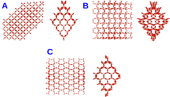
Due to the lack of information in the literature about the possible atomic structures of small diameter SiO2 nanowires we have approached the problem from a heuristic point of view. As a reasonable initial choice we constructed SiO2 nanowires based on one dimensional-like fragments of the most stable bulk phases. A number of polymorphs of silica, SiO2, exist in nature. Coesite and stishovite are polymorphs which form at high pressure and temperature. At moderately lower temperatures one finds the tridymite and cristobalite crystalline forms. These, like quartz, present low and high-temperature structural modifications. The crystalline lattices of three of those phases, -cristobalite 29, ortho-tridymite 30, and -tridymite 31 are plotted in 1. According to this, we have adopted as starting nanowire geometries fragments of the -cristobalite, ortho-tridymite, and -tridymite crystals in the form of SiO2 nanowires. Those fragments are of infinite length in the direction of the nanowire axis. The unit cell contains six SiO2 units in the case of the -cristobalite nanowire, and twelve SiO2 units in the two tridymite wires. Dynamical relaxations led to the optimized structures of 2, where frontal and lateral views of the most stable nanowires are shown. 2 also shows a front view of the starting bulk-like nanowires before relaxation. Molecular dynamics simulations revealed that the minimum energy structures obtained are robust and stable up to 500K at least. Optimization of the cell parameter in the axial direction was also allowed, but no significant variations were observed with respect to the starting cell parameters. The calculated lattice parameters are 5.07 Å, 8.27 Å and 8.24 Å for the -cristobalite, -tridymite and ortho-tridymite-based SiO2 nanowires, respectively. The starting bulk-like nanowires present a hexagonal-like section with some oxygen atoms popping out due to stoichiometry. The section deforms after structural relaxation: the hexagonal inner cavity of the nanowire reduces its size and more oxygen atoms appear on the outer part of the nanowire. The reconstruction is more severe in the two tridymite nanowires. We also did calculations in which the wires were cut from the crystal choosing other directions for the wire axis. However, those led to less stable structures after optimization.
| (Å) | (Å) | (Å) | |||||||
|---|---|---|---|---|---|---|---|---|---|
| Bulk-based | |||||||||
| -cristobalite | 5.03 | 6.73 | 1.730.06 | ||||||
| Ortho-tridymite | 6.31 | 8.74 | 1.740.08 | ||||||
| -tridymite | 6.43 | 8.45 | 1.740.08 | ||||||
| Rutile-based | |||||||||
| 4 SiO2 units | 4.67 | 6.57 | 1.730.02 | ||||||
| 12 SiO2 units | 10.32 | 12.23 | 1.740.05 | ||||||
| 16 SiO2 units | 14.12 | 15.64 | 1.740.04 | ||||||
| 24 SiO2 units | 16.09 | 17.84 | 1.730.05 | ||||||
| 32 SiO2 units | 18.67 | 21.16 | 1.740.06 | ||||||
| 40 SiO2 units | 23.04 | 24.88 | 1.740.08 |
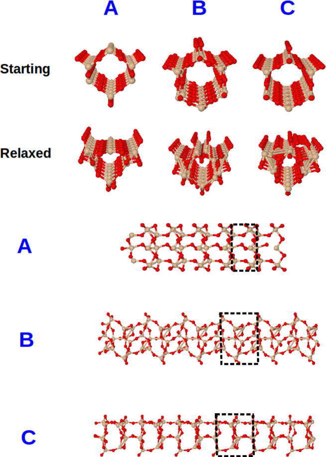
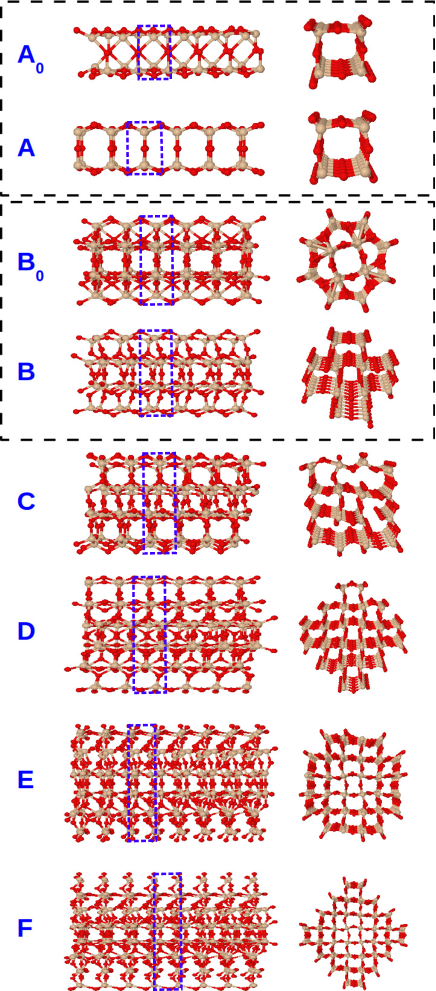
We have performed additional calculations starting with other structures. For this purpose we first took a narrow SiO2 nanowire whose lateral and front views are shown in panel A0 of 3. That structure, having four SiO2 molecules per unit cell, is taken from previous works 9, 10 on nanowires of transition metal dioxides (MO2), and it was obtained by relaxing nanowires cut from the rutile crystals. Shown in panel A is the relaxed SiO2 nanowire, whose structure is more symmetric than that of the starting nanowire. Next we relaxed a nanowire with the form of a two-wall nanotube, whose lateral and front views are shown in panel B0 of 3. This structure was also taken from previous work on transition metal dioxide nanowires 9, 10. Structural relaxation distorts the original nanotube producing an atomic arrangement based on the rutile lattice (panel B). Motivated by this feature, we explore a growth pattern to construct thicker nanowires based on the rutile-like structure of panel A. Nanowires with 16, 24, 32 and 40 SiO2 units per cell are shown in panels C, D, E and F. These structures are shown after relaxation. For nanowires of a given size, different starting configurations were considered, but only those leading to the most stable nanowires are shown in 3. The structures of all these nanowires are stable in molecular dynamics simulations at 500K.
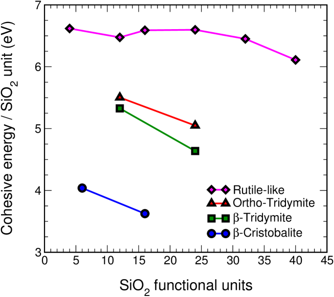
The cohesive energies of these nanowires per SiO2 unit, defined as:
| (1) |
have been plotted versus the number of SiO2 molecules per unit cell in 4. In (1), is the total energy of the nanowire per unit cell, is the number of SiO2 molecules per unit cell, and is the total energy of an isolated gas-phase SiO2 molecule. The cohesive energies of the reconstructed ortho-tridymite and -tridymite nanowires are similar, and higher than the cohesive energy of the reconstructed -cristobalite nanowires. That is, the tridymite nanowires are more stable.
In order to check the validity of the structures obtained in the simulations using the canonical (minimal) unit cell, we have carried out calculations taking a cell doubled in size, along the nanowire axis, compared to the original one. The aim of the test was to allow for the possibility of observing new structural reconstructions not seen in the dynamical quenches based on the minimum unit cell. The test was made for all the bulk-based nanowires and four rutile wires. The results obtained do not reveal any significant variation of the structures with respect to the nanowires obtained by just using the minimum unit cell.
The cohesive energies of the rutile-based nanowires are also included in 4. A similar value of the cohesive energy per SiO2 unit is obtained for all the rutile-based nanowires, although it tends to decrease as the cross section of the nanowire increases. That is, the cohesive energy per SiO2 unit tends to decrease for thick nanowires. We think this is due to the fact that no stable bulk phases of SiO2 with structures related to rutile exist at normal pressures. The only bulk phase related to rutile is stishovite 32, a high pressure phase with a mass density of 4.29 g cm-3, much larger than the density of -quartz, 2.65 g cm-3. Consequently, thick rutile-like nanowires are not expected to form at normal pressure. Thin nanowires, like those studied here, present fewer problems because the structural constraints are weaker. Still, one can notice the enhanced stability of the rutile-like nanowires with respect to those obtained from the -cristobalite, ortho-tridymite and -tridymite phases. The gain in cohesive energy with respect to the tridymite-like nanowires with a similar number of SiO2 units ranges between 1 eV and 2 eV per SiO2 unit, and from 2.5 and 3 eV per SiO2 unit with respect to the -cristobalite-like nanowire.
To interpret the behaviour of the cohesive energies in 4 one has to notice that the range of cross sections for these nanowires corresponds to the non-scalable regime, well known in clusters 33, where the properties vary in a non-smooth way, often showing oscillations, as the cluster size increases. The present calculations suggest that the non-scalable regime occurs also in thin nanowires, and is responsible for the oscillations of the cohesive energy of the rutile-like wires, and for the initial decrease of the cohesive energies of the -cristobalite, ortho-tridymite and -tridymite wires.
Basic structural measurements of a nanowire can include its diameter as well as its length. These parameters may be related to laboratory preparation of nanowires 14, 15, 16. At the atomistic level, a characteristic parameter would be an average bond-length. Accordingly, 1 provides the calculated average diameter estimated from the most external radially opposite Si atoms, , the average diameter estimated from the most external radially opposite O atoms, , and the average Si-O bond-distance, , in all the bulk-based and rutile-based SiO2 nanowires. Notice that the largest diameter obtained is that for in the case of 40 functional units per unit cell. Its value is about 25 Å=2.5 nm, which, from the point of view of experimental synthesis, corresponds to a thin nanowire. Although SiO2 nanowires used as a core in composite systems such as RuO2/SiO2 have tipically been one order of magnitude thicker 14, there is no reason why smaller core nanowires could not be processed and employed. Since the thicknesses of the nanowires studied here are on the non-scalable regime, where the properties may vary in a non smooth way, it is not easy to extrapolate the results of 4 to very thick wires.
4 ELECTRONIC STRUCTURE
4.1 Density of states (DOS)
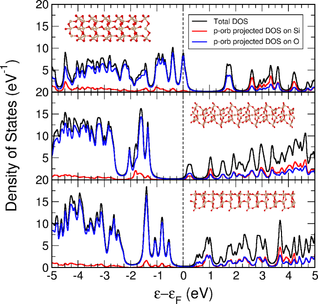
We begin our analysis by considering the nanowires obtained from the cristobalite and tridymite bulk-phases (see 2). In addition to its intrinsic interest, the study provides insight on how structural changes in the nanowires may affect their electronic properties, bonding character and charge transfer between atoms. Such information could prove useful when trying to form SiO2 semiconducting nanostructured materials, as well as when forming composite nanocables with overlying metal or semiconducting materials.
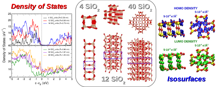
5 shows the total electronic DOS profiles versus energy for the three nanowires of 2. In order to mimic the experimental resolution 34, a Lorentzian broadening of 0.05 eV has been applied to the energy levels. The magnitude of the electronic gaps, measured as the difference between the energies of the highest occupied (HOMO) and lowest unoccupied (LUMO) molecular orbitals, is 1.69, 1.57 and 1.06 eV for the -cristobalite (top panel), ortho-tridymite (middle panel) and -tridymite (bottom panel) nanowires, respectively, revealing the potential semiconducting-like character of these nanostructures, especially if appropriate donor or acceptor atoms were available to reside in shallow states below the band edges within the bandgap. The calculated band-gaps are smaller than the gaps of the corresponding bulk crystals. The gap of bulk -cristobalite obtained by DFT is in the range 5.5-5.7 eV for LDA calculations, and increases to 10.1-10.3 eV if quasiparticle corrections are taken into account 35. A gap of 6.6 eV is obtained in gradient-corrected BLYP calculations 36. Our RPBE calculations give a gap of 7 eV. Turning to the tridymite crystals, the BLYP gap of -tridymite is 6.6 eV 36, and our RPBE gaps for ortho- and -tridymite are 5.8 and 7.7 eV, respectively. That is, the bulk phases are insulators. A substantial lowering of the gap of the nanowires with respect to the bulk crystals is then obtained. The band-gap values of the nanowires are similar to those for some elemental bulk semiconductors like Si, or III-V binary and ternary semiconductor compounds, like GaAs, InGaP, and InGaAs, with varying stoichiometry 37, 38, 39.
Regarding the DOS profiles of the three nanowires we observe different band structure behaviors: i) the -cristobalite nanowire (top panel) acts as a pure acceptor semiconductor-like material, able to give up mobile holes whose volumetric density is
| (2) |
since (here is the top of the valence band, is the Boltzmann constant and is a numerical constant depending on the temperature ); ii) the ortho-tridymite nanowire (middle panel) acts as a potential donor semiconductor-like material, able to create mobile electrons with density
| (3) |
since (here is the bottom of the conduction band and is a numerical constant depending on ); and iii) the -tridymite nanowire (bottom panel) acts as an intrinsic semiconductor with tiny carrier densities
| (4) |
with the Fermi level located in the middle of the gap
| (5) |
for 0 or 1, and with no preference to donate or accept electronic charge 40.
In 5 we also show the projected DOS onto the -states of Si and O atoms. In the energy range plotted, the occupied part of the DOS is dominated by the -states of O. This means that the oxygen atoms have accepted some electronic charge from the silicon atoms (details are provided below). The sum of the Si and O -orbital contributions falls slightly below the total DOS, the difference being the smaller -orbital contributions.
| Transport gaps (eV) | Standard DFT | quasi-particle G0W0 | GW + BSE |
|---|---|---|---|
| Rutile-like nanowire | |||
| 4 SiO2 units | 4.53 | 4.80 | 5.98 |
| 12 SiO2 units | 2.84 | 2.98 | 3.58 |
| 16 SiO2 units | 1.62 | 1.73 | 2.01 |
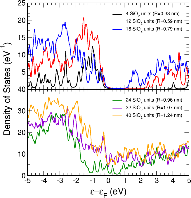
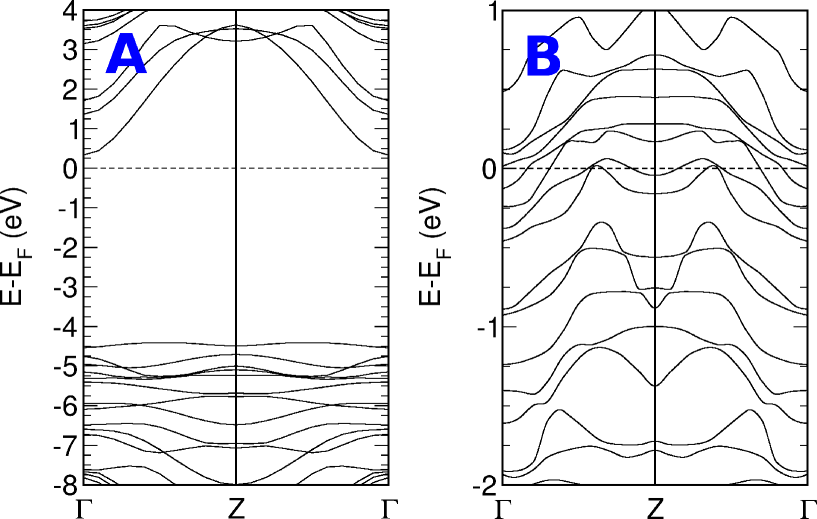
6 shows the total DOS profiles versus energy for the most stable rutile-based nanowires of 3. As observed in the top panel of 6, thin rutile-like nanowires (with 4, 12 and 16 SiO2 molecules per unit cell) show a semiconducting behavior, and the electronic gap is progressively reduced as the number of SiO2 functional units in the cell increases. For thicker nanowires, those in the bottom panel, new peaks appear in the DOS near the Fermi energy, and this region becomes congested. The structure of the electronic levels in that region can be seen in 7. That figure shows the band structure of two nanowires, with 4 and 24 SiO2 functional units in the cell, respectively. The left-side panel shows clearly the gap existing in the thin nanowire. On the other hand, the band structure of the thick nanowire (notice the different energy scale) shows that a bunch of states occupy the region of the gap. These can be interpreted as surface-like states.
A comparison between 5 and 6 shows differences between the electronic gaps corresponding to nanowires of similar thickness but different structures. The -cristobalite nanowire (with four SiO2 units per cell) has a gap of 1.69 eV, while the gap of the thinnest rutile-like nanowire (six SiO2 units per cell) is 4.93 eV. For nanowires with 12 SiO2 units per cell, the differences are again evident, although not so large: the rutile-like nanowire has a gap of 2.91 eV, and the two tridymite nanowires show gaps of 1.57 and 1.06 eV. The conclusion is that by varying the thickness and the structure of the nanowires, these can be engineered to produce a desired value of the electronic gap.
There is a reduction of the band-gap of the nanowires with respect to the SiO2 bulk crystals. We ascribe the difference to the particular structure of the nanowires, with many unsaturated oxygen atoms on the surface. This is required by stoichiometry, two O atoms per Si atom, and it becomes reflected, as shown in 5, in the dominance of the occupied DOS near the Fermi level by the -like states of oxygen. The reduced gaps also indicate that the nanowires will be more reactive than the usual bulk SiO2 phases.
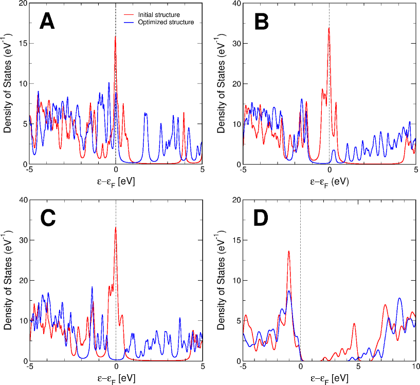
The structural relaxation of the nanowires shown in 2 and 3 is well explained by looking at the DOS. 8 shows the DOS profiles of four nanowires in the original unrelaxed structure and after structural optimization. In the cases of -cristobalite (panel A), ortho-tridymite (panel B) and -tridymite (panel C), the density of states in the unrelaxed structure shows several high peaks in the region near the Fermi energy. Those peaks correspond to electronic states located inside a gap of width about 5 eV, which reminds the gap in the bulk crystals. The high DOS near the Fermi energy indicates that the unrelaxed structures of the nanowires are unstable. In fact, as the initial structures of 2 relax to more stable arrangements, the states at the Fermi level almost disappear, and a true gap develops, although smaller in magnitude than the original gap of the crystal. At difference with the previous wires, the smallest rutile-based nanowire shows a gap and no peaks at the Fermi energy. The effect of structural relaxation is, in this case, to widen the gap by moving the unoccupied electronic states up in energy. The widening of the gap increases the stability of the nanowire. However, as discussed above, surface states appear in the gap for thick rutile-like nanowires.
In order to check the reliability of the DFT-DOS profiles and transport gaps, we have carried out more accurate electronic structure calculations for the rutile-based nanowires with 4, 12 and 16 functional units. The choice of these testing structures is based on: i) their transport gaps are easy to identify (see 6), while the thicker nanowires show states inside the gap region; ii) their small cell sizes lower the substantial computational effort of such calculations. For this purpose, we have calculated the many-body corrections using two different formalisms: a) quasi-particle corrections have been calculated within the G0W0 formalism 41, 42 (quasi-particle Green function screened interaction approach) to properly account for the exchange-correlation self-energy; b) the GW + Bethe-Salpeter equation (BSE) approximation 43, 44, 45, where the quasi-particle GW approach is further corrected to account for excitonic effects (electron-hole interation) in the unoccupied and excited states. The GW + BSE formalism includes, by construction, excitonic effects, which are important in highly correlated systems, and combines the excellent performance of the GW + standard DFT approach for the ground state electronic structure with the high accuracy of the BSE methodology for the calculation of excitations. These calculations have been carried out with the Yambo package 46. More than 200 unoccupied electronic bands were necessary to obtain converged self-consistent results.
2 shows the transport gaps (in eV) predicted by the G0W0 and GW + BSE formalisms for the three rutile-like nanowires. The comparison between the DFT and G0W0 gaps indicates that the first-order quasi-particle corrections are small: the G0W0 gaps are larger than the DFT gaps by 0.27, 0.14 and 0.11 eV for the nanowires with 4, 12 and 16 SiO2 units, respectively. The excitonic corrections are larger. These lead to an additional increase of the gap by 1.18, 0.60 and 0.28 eV for the same three nanowires, respectively. The percentage change of the gap due to self-energy corrections,
| (6) |
is nearly independent of wire diameter (about 6 %). On the other hand, the additional percentage change induced by excitonic effects,
| (7) |
decreases as the nanowire diameter increases: 25 %, 20 % and 16 %, for the three nanowires, respectively. Thus, the largest gap corrections due to many-body effects occur for the thinnest nanowires. It is worth noticing, however, that the trend of a decreasing gap with increasing nanowire diameter predicted by the standard DFT calculations is maintained after including many-body corrections.
4.2 Electron distribution and charge transfer
| -cristobalite | Ortho-tridymite | Rutile | |
|---|---|---|---|
| Si atom | |||
| orbital charge | 1.1 | 1.0 | 1.0 |
| orbital charge | 2.2 | 2.2 | 2.2 |
| Net charge gain / lost | -0.7 | -0.8 | -0.8 |
| O atoms | |||
| orbital charge | 3.4 | 3.4 | 3.3 |
| orbital charge | 9.3 | 9.4 | 9.5 |
| Net charge gain / lost | 0.7 | 0.8 | 0.8 |
In order to understand the bonding mechanism we have carried out an analysis of the electronic charges of the atoms. Theoretical calculations giving the electronic charge distribution in the system can, in principle, provide this type of information, but the way to extract it is not unique. The usual output of quantum mechanical calculations is a continuous electronic charge density and it is not evident how to partition electrons amongst fragments of the system such as atoms or molecules. Different schemes have been proposed, some of them based on localized electronic orbitals 47, 48 and others based on the electron density 49.
Taking advantage of the localized basis set used in the Fireball code, we can evaluate the electronic charge in each localized orbital at the end of the self-consistent calculation 19, 22, 23. The Löwdin method 47, 48 has been employed to obtain the orbital charges. With those values, the sign and the magnitude of the net charge transfer between atoms can be obtained. In order to check the accuracy of the results we have compared the atomic charges with the Bader atomic charges 49, obtained using electron densities from the plane-wave Dacapo code. There is excellent agreement between atomic charges calculated in the two ways.
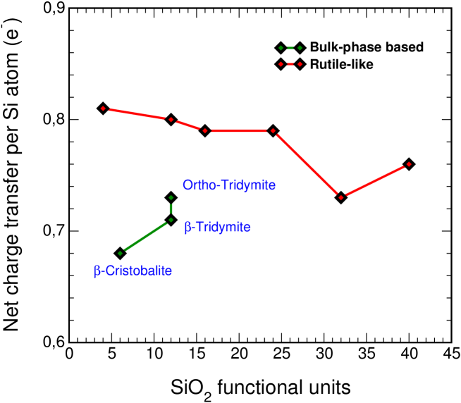
Electronic charge is transferred from Si to O atoms due to the higher electronegativity of oxygen. 9 shows the average net charge transfer, in e- units, from Si to O atoms, per SiO2 unit. In other words, this is the average charge transfer per Si atom. Charge transfers in the rutile-like nanowires range between 0.73 and 0.81 e- per Si atom. These are slightly larger than the charge transfers in the cristobalite- and tridymite-like nanowires, 0.68-0.73 e-. The larger charge transfer in the rutile-like nanowires correlates with their higher stability. For this purpose, one can notice the qualitative similarity of the data in 4 and 9.
3 shows average and orbital charges, in e- units, in the Si and O atoms for three nanowires: -cristobalite and ortho-tridymite wires, and the rutile-like nanowire with 24 SiO2 units per cell. The net electronic charges lost (by each Si atom) or gained (by two O atoms) are also given. The results for the two tridymite-like nanowires are very similar. Also the results for the six rutile-like nanowires are very similar. This, plus the information in 3, indicates that the average atomic charge populations, total and orbital-resolved, are similar in all the nanowires. We then conclude that the chemical bonding in these nanowires exhibits common features, quite independent of the detailed structure of the nanowires.
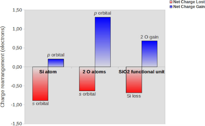
The chemical bonding can be described as a mixture of covalent and ionic contributions. In all cases, the -like electron population of the O atoms gains 0.70-0.75 e- per O atom (1.4-1.5 e- per SiO2 unit). The Si atoms also increase their -like charge by 0.1-0.2 e- per atom. This general increase of -like population in the nanowires arises from a loss of charge in the -like orbitals (0.9 e- lost by the Si atoms and 0.30-0.35 e- lost by each O atom). This is summarized in the bar diagram of 10 for the -cristobalite nanowire.
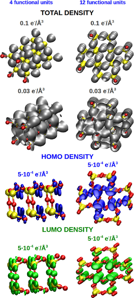
In order to visualize the spatial distribution of the electronic charge, 11 shows surfaces of constant electron density in 3 dimensional perspective for the rutile-like nanowires with 4 and 12 SiO2 units per cell. The densities selected are 0.1, and 0.03 e. The results are similar for the two nanowires (and for others not shown here). The surfaces corresponding to a density of 0.1 e are formed by a set of disconnected pieces showing a concentration of charge around the oxygen atoms, aided by the charge transfer from Si to O atoms. The surface corresponding to the lower density, 0.03 e, is a connected surface displaying the mixture of ionic and covalent bonding in the nanowires. 11 also shows the charge densities of the HOMO and LUMO orbitals, again for the rutile-like nanowires with 4 and 12 SiO2 units per cell (all with values of 510-4 e). In the thin nanowire, the HOMO orbital is localized near the planes formed by the most external oxygen atoms (each of those planes contains four oxygen atoms). In contrast, the LUMO orbital is localized near the planes containing the distorted squares formed by four Si and four O atoms. For the thicker nanowire, the HOMO orbital is placed in between the planes containing the Si atoms, and the LUMO orbital mostly surrounds internal Si atoms.
5 SUMMARY
This work presents ab-initio simulations for SiO2 nanowires. The structures of the nanowires have been determined: i) by relaxing nanowires cut from SiO2 bulk crystals (-cristobalite, ortho-tridymite and -tridymite), and ii) by relaxing nanowires with a rutile-like structure. The analysis of the electronic states indicates that many of these nanowires have a semiconducting character, different from the insulator character of the macroscopic bulk-crystals. However, for the thick rutile-like nanowires we found the gap congested by the presence of surface states. The bonding in all the nanowires can be described as partly ionic and partly covalent. Novel uses for nanoscopic SiO2 nanowires may arise from insights gained about the electronic density of states, chemical bonding, charge density distribution and cohesive energies per SiO2 unit as a function of nanowire thickness and structure.
6 ACKNOWLEDGEMENTS
Results presented here were conducted under the aegis of the NRL NanoScience Institute (NSI), project ”Nanoparticulate Ruthenium Dioxide Shells on Dielectric Cores: Basic ElectroChemistry, Physics, and Material Science of a Single-Unit-Thick Electron Conductor and the Implications for Energy and Electro-Optical Applications”. The work was supported by Spanish MICINN and the European Regional Development Fund (grants MAT2008-06483-C03-01, MAT2011-22781 and FIS2010-16046), Junta de Castilla y León (grant VA158A11-2), CAM (grant S2009/MAT-1467), and the European Project MINOTOR (Grant FP7-NMP-228424). J.I.M. acknowledges funding from Spanish MICIIN through Juan de la Cierva Program.
References
- 1 Heller, A. Science 1984, 223, 1141-1148.
- 2 Murphy, J.; Srinivasan, S.; Conway, B. E. Electrochemistry in Transition: From the 20th to the 21st Century; Plenum: New York, 1992.
- 3 Khaselev, O.; Turner, J. A. Science 1998 280, 425-427.
- 4 Grätzel, M. Nature 2001 414, 338-344.
- 5 Whitesides, G. M.; Crabtree, G. W. Science 2007 315, 796-798.
- 6 Hemminger, J.; Crabtree, G. W.; Kastner, M. The Energy Challenges Report: New Science for a Secure and Sustainable Energy Future; Argonne National Laboratory: Argonne, IL, 2008.
- 7 Man, I. C.; Su, H.; Calle-Vallejo, F.; Hansen, H. A.; Martínez, J. I.; Inoglu, N. G.; Kitchin, J.; Jaramillo, T. F.; Nørskov, J. K.; Rossmeisl, J. ChemCatChem 2011 3, 1159-1165.
- 8 Martínez, J. I.; Hansen, H. A.; Rossmeisl, J.; Nørskov, J. K. Phys. Rev. B 2009 79, 045120(1)-045120(5).
- 9 Mowbray, D. J.; Martínez, J. I.; García-Lastra, J. M.; Thygesen, K. S.; Jacobsen, K. W. J. Phys. Chem. C 2009 113, 12301-12308.
- 10 Mowbray, D. J.; Martínez, J. I.; Calle-Vallejo, F.; Rossmeisl, J.; Thygesen, K. S.; Jacobsen, K. W.; Nørskov, J. K. J. Phys. Chem. C 2011 115, 2244-2252.
- 11 Chervin, C. N.; Lubers, A. M.; Pettigrew, K. A.; Long, J. W.; Westgate, M. A.; Fontanella J. J.; Rolison, D. R. Nano Lett. 2009 9, 2316-2321.
- 12 Krowne, C. M. Phys. Lett. A 2010 374, 614-619.
- 13 Krowne, C. M. Phys. Lett. A 2010 374, 1172-1179.
- 14 Krowne, C. M. J. Nanomater. 2010 2010, 160639(1)-160639(27).
- 15 An, X.; Meng, G. W.; Wei, Q.; Kong, N.; Zhang, L. D. J. Phys. Chem. B 2006 110, 222-226.
- 16 Li, F. J.; Zhang, S.; Kong, J. H.; Zhang, W. L. Nanosci. Nanotech. Lett. 2011 3, 240-245.
- 17 Bilalbegovic, G. J. Phys.: Condens. Matter 2006 18, 3829-3836.
- 18 Zhang, D. J.; Guo, G.; Liu, C. B.; Zhang, R. Q. J. Phys. Chem. B 2006 110, 23633-23636.
- 19 Lewis, J. P.; Jelínek, P.; Ortega, J.; Demkov, A. A.; Trabada, D. G.; Haycock, B.; Wang, H.; Adams, G.; Tomfohr, J. K.; Abad, E.; Wang, H.; Drabold, D. A. Phys. Stat. Sol. B 2011 248, 1989-2007.
- 20 Hammer, B.; Hansen, L. B.; Nørskov, J. K. Phys. Rev. B 1999 59, 7413-7421.
- 21 Bahn, S. R.; Jacobsen, K. W. Comput. Sci. Eng. 2002 4, 56-66.
- 22 Lewis, J. P.; Glaesemann, K. R.; Voth, G. A.; Fritsch, J.; Demkov, A. A.; Ortega, J.; Sankey, O. F. Phys. Rev. B 2001 64, 195103(1)-195103(10).
- 23 Jelínek, P.; Wang, H.; Lewis, J. P.; Sankey, O. F.; Ortega, J. Phys. Rev. B 2005 71, 235101(1)-235101(9).
- 24 Harris, J. Phys. Rev. B 1985 31, 1770-1779.
- 25 Foulkes, W. M. C.; R. Haydock, Phys. Rev. B 1989 39, 12520-12536.
- 26 Fuchs, M.; Scheffler, M. Comput. Phys. Commun. 1999 119, 67-98.
- 27 Vanderbilt, D. Phys. Rev. B 41, 7892-7895 (1990).
- 28 Chadi, D. J.; Cohen, M. L. Phys. Rev. B 1973 8, 5747-5753.
- 29 Wyckoff, R. W. G. Crystal Structures, Vol. 1; Interscience, John Wiley and Sons: New York, London, 1963.
- 30 Dollase, W. A. Acta Cryst. 1967 23, 617-623.
- 31 Kihara, K. Z. Kristallogr. 1978 148, 237-253.
- 32 Ross, N. L.; Shu, J. F.; Hazen, R. M.; Gasparik, T. Am. Mineralogist 1990 75, 739-747.
- 33 Alonso, J. A. Structure and Properties of Atomic Nanoclusters; Imperial College Press: London, 2011.
- 34 Martínez, J. I.; Castro, A.; Rubio, A.; Alonso, J. A. J. Comput. Theor. Nano. 2006 3, 761(1)-761(6).
- 35 Ramos, L. E.; Furthmüller, J.; Bechstedt, F. Phys. Rev. B 2004 69, 085102(1)-085102(8).
- 36 Gnani, E.; Reggiani, S.; Colle, R.; Rudan, M. IEEE Trans. Elec. Dev. 2000 47, 1795-1803.
- 37 Sze, S. M. Physics of Semiconductor Devices; John Wiley and Sons: New York, 1981.
- 38 Jenichen, A.; Engler, C. Phys. Stat. Sol. B 2010 247, 59-66.
- 39 Picozzi, S.; Continenza, A.; Asahi, R.; Mannstadt, W.; Freeman, A. J.; Wolf, W.; Wimmer, E.; Geller, C. B. Phys. Rev. B 2000 61, 4677-4684.
- 40 McKelvey, J. P. Solid State and Semiconductor Physics; Harper & Row: New York, 1966.
- 41 Hybertsen, M. S.; Louie, S. G.; Phys. Rev. Lett. 1985 55, 1418-1421.
- 42 Hybertsen, M. S.; Louie, S. G.; Phys. Rev. B 1986 34, 5390-5413.
- 43 Rohlfing, M.; Louie, S. G. Phys. Rev. Lett. 1999 83, 856-859.
- 44 Onida, G.; Reining, L.; Rubio, A.; Rev. Mod. Phys. 2002 74, 601-659.
- 45 Martínez, J. I.; García-Lastra, J. M.; López, M. J.; Alonso, J. A. J. Chem. Phys. 2010 132, 044314(1)-044314(5).
- 46 Marini, A.; Hogan, C.; Grüning, M.; Varsano, D.; Comput. Phys. Commun. 2009 180 1392-1403.
- 47 Cusachs, L. C.; Politzer, P. Chem. Phys. Lett. 1968 1, 529-531.
- 48 Löwdin, P. O.; Adv. Quantum Chem. 1970 5, 185-199.
- 49 Bader, R. F. W. Atoms in Molecules - A Quantum Theory; Oxford University Press: New York, 1990.