Surface adatom conductance filtering in scanning tunneling spectroscopy of Co-doped BaFe2As2 iron pnictide superconductors
Abstract
We establish in a combination of ab initio theory and experiments that the tunneling process in scanning tunneling microscopy/spectroscopy on the A-122 iron pnictide superconductors - in this case BaFe2-xCoxAs2 - involve a strong adatom filtering of the differential conductance from the near- Fe3d states, which in turn originates from the top-most sub-surface Fe layer of the crystal. The calculations show that the dominance of surface Ba-related tunneling pathways leaves fingerprints found in the experimental differential conductance data, including large particle-hole asymmetry and an energy-dependent contrast inversion.
pacs:
74.70.Xa,73.40.Gk,73.20.-rThe discovery of high-temperature superconductivity in the iron pnictides has prompted a tremendous effort directed towards understanding the nature of superconductivity in these systems. Theory indicates unconventional superconductivity but with a pairing symmetry that can be very sensitive to electronic and structural details of the system PeterReview . Experimentally, surface sensitive probes of the electronic structure such as angle-resolved photoemission spectroscopy (ARPES) TerashimaPNAS ; KoitzschPRL2009 ; WiPNAS2011 ; EvHPRL2011 and scanning tunneling microscopy/spectroscopy (STM/STS) Hoffman ; MasseePRB2009 ; MasseeEPL2010 ; ZhangPRB2010 ; ChuangScience2010 ; NascimentoPRL2009 ; YinPRL2009 , play a major role in the search for a microscopic understanding of the superconductivity in these systems. In this context, the alkaline-earth-metal AFe2As2 (A-122, A = Ca, Ba, Sr) iron pnicties have been widely studied due to the availability of high-quality crystals, and the possibility to both n- and p-type dope these systems. It is therefore essential to definitively establish the properties of A-122 surfaces. Accessing the underlying physics representative of the bulk relies on a quantitative understanding of surface-related matrix elements coupled to potential surface-related changes in electronic/structural properties and this is exactly what we aim to do here.
Perhaps the most prominent theater for the surface/bulk debate is the case of BaFe2-xCoxAs2 (Ba-122) Hoffman . Due to the strong covalent bonding within the AsFe2As block, the surface of cleaved Ba-122 is expected to be either an exposed FeAs layer or a half layer of Ba atoms. Although there are indications for the former NascimentoPRL2009 , there is a much larger body of evidence for the latter EvHPRL2011 ; MasseePRB2009 ; MasseeEPL2010 ; ZhangPRB2010 ; YinPRL2009 . Electrostatics would dictate a half Ba layer as the crystal termination. Both the strong temperature dependence of the reconstructed surface and the large variety of topographic images observed by STM MasseePRB2009 ; Hoffman are most easily understood in terms of relatively loosely bound Ba atoms (which could be considered adatoms) constituting the termination layer. Density functional theory (DFT) data point to a Ba termination with a or 1 reconstruction as energetically favorable GaoPRB2010 . Recently, a combined LEED/ARPES/DFT study showed that the experimental LEED I/V curves could only result from a reconstructed Ba surface and furthermore that the associated surface-related bands overlapping with the bulk states have a strong impact on the breadth of spectral features observed in ARPES for this system EvHPRL2011 .
A quantitative understanding of tunneling processes in complex, layered crystals is important, as is illustrated in the cuprate high Tc systems, where asymmetry between electron removal and addition in STS data is seen as a sign of strong correlation effects HanaguriNature2004 , as well being attributed to the effect of the specific tunneling pathway from the CuO2 plane LDOS through the SrO and BiO layers to the STM tip NieminenPRL2009 . Given the marked and surface reconstructions observed in the LEED and STM experiments on the A-122 pnictide family Hoffman , it is important to uncover the impact of the real surface structure on spectroscopic tunneling measurements themselves.
We tackle this issue here by theoretically establishing the precise role of the Ba surface in STS of Co-doped Ba-122 superconductors, showing that the surface Ba atoms strongly filter the tunneling current, leading to marked particle-hole asymmetry in the tunneling conductance and bias-dependent contrast inversion in maps. A direct comparison with experiment explicitly confirms these key predictions.
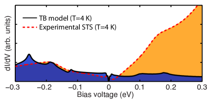
We start by examining the tunneling conductance in a simplified Fe band-based model, incorporating the five-band tight-binding model of Graser et al. Graser and comparing the results to the experimental data. This model was obtained by fitting to DFT calculations and so an additional two-fold renormalization of the bands is included to account for electronic correlations. As a next step, superconductivity is introduced at the BCS level, including interband impurity scattering. Since the interest here is in over energy scales almost 100 times that of , the precision of the theoretical description of the superconductivity is non-critical Supplement . Fig. 1 compares the model to measured spectra obtained on an overdoped sample (x = 0.22 i.e. 11% doping, Tc = 12 K). On the occupied side - negative sample bias - the gross structure is reproduced by the model, and one might assign the broad peak in the STS trace at meV to features in the Fe-based DOS. However, the unoccupied states raise doubts as to whether such a simple interpretation is tenable, as the measured exhibits a large particle-hole asymmetry with a much larger signal at positive bias voltage, a characteristic wholly lacking in the data of the tight-binding model. This discrepancy cannot be removed by including additional self-energy effects as they would only serve to further broaden the spectral features. It is clear that the theory needs to leave the confines of the five Fe-band basis, and the remainder of this letter is devoted precisely to this, showing that recognizing the filtering effect of the surface Ba states on the tunnel current removes the discrepancy so visible in Fig. 1.
To model the tunneling process correctly we have performed DFT calculations to simulate tunneling into various finite slab geometries of 8.5% () Co-doped Ba-122. These calculations use the full potential local orbital code (FPLO), FPLO , in the scalar-relativistic and local density approximations (LDA) pw92 . The choice of functional is not critical, since we are considering the non-magnetic state and fixed atomic geometries. See Supplement for further computational details.
The Ba-122 surface is modeled using a slab structure with a 21 reconstructed, half Ba termination layer with the atomic positions fixed to LEED data EvHPRL2011 . Since STM/STS experiments are often performed with Pt/Ir tips, we model the tip with a single Pt atom (henceforth referred to as the ‘tip’), positioned at different locations above the sample. The tunneling conductance is calculated from a weighted overlap between the slab wave functions and the localized 6 and 5 states of the tip atom:
| (1) |
where is the discrete tip state with energy , and is the Fermi level of the slab. The function representing the tip density of states (DOS) is replaced with a Lorentzian broadened expression, mimicking band formation in a real macroscopic tip. Here we used eV for all tip states, noting that the exact value has no qualitative influence on the results, and merely results in a scaling of the magnitude of the resulting curves. Eq. (1) is essentially a version of the Todorov-Pendry approximation Pendry91 as has been used in a wave function context Kobayashi95 and a Green’s function context Suominen11 . It goes beyond the commonly used Tersoff-Hamann model tersoff85 , which is derived for -wave tips only.
The matrix element in Eq. (1) in its full form is , with the potential at the tip. However, our tests have shown that for a nearly spherical potential the effect of including also only results in a global rescale of the curves, and thus the form shown in Eq. (1) is sufficient.
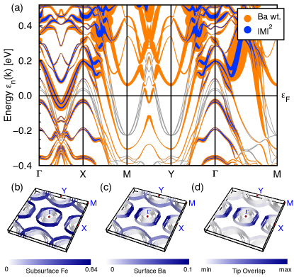
We first consider the matrix element for tunneling between the tip and the sample . Fig. 2(a) plots the band structure for the 1 reconstructed slab, with numerous surface bands from reconstruction-induced back-folding and atomic distortions in the outermost As-Fe2-As block EvHPRL2011 . The thickness of the orange (light) shading codes for the weight associated with the surface-Ba character of the bands. Most of the Ba-dominated bands lie above , except for one band with Ba- character dipping below between and . The magnitude of the tip-sample matrix element , coded by the weight of the blue (dark) shading, is also shown in Fig. 2(a). Comparing the two shadings, it is clear that the largest tunneling matrix elements coincide with the presence of bands with strong surface Ba character. To illustrate this important finding, panels (b)-(d) of Fig. 2 show the Fermi surface of the slab. In panel (b) the blue shading codes the sub-surface Fe 3d character, in (c) the Ba surface character and in (d) the tunneling matrix element . Panel (c) reflects the surface reconstruction, in that the Ba projection clearly breaks C4 symmetry. The essential point here is that panels (c) and (d) strongly resemble each other, meaning regions of the Fermi surface with the largest surface-Ba weight are directly correlated with the largest tunneling matrix element. In contrast, the weight of the Fe atoms is isotropic around the Fermi surfaces (Fig. 2[b]) and does not correlate with the suppressed tunneling matrix element along the - direction evident in panel (d). At low bias voltage, the primary tunneling pathway is in fact one from the uppermost Fe layer of the terminating As-Fe2-As block to the tip, and this runs through the Ba surface atoms, involving the - region of the Brillouin zone. It is through this filter that STS-experiments see the superconducting states of these materials.
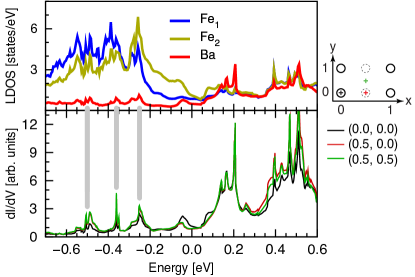
Having established the clear correlation between the tunneling matrix element and Ba character of the bands, we now turn to the calculated tunneling conductance itself. In Fig. 3 the calculated spectra obtained for various tip locations above the 1 terminated A-122 (A=Ba) surface are shown. In simple models is expected to be a measure of the local DOS of the sample at the tip position and so the partial DOS, projected on the surface Ba atoms and two representative sub-surface Fe atoms is plotted in the upper panel. Inspecting the lower panel of the figure, the first observation is that the calculated spectra exhibit a large bias asymmetry, with tunneling into unoccupied states of the sample clearly being favored, regardless of the exact tip position. Thus, consideration of rather than LDOS now brings the theory into line with the experimental data (Fig. 1) in terms of tunneling asymmetry. Furthermore, the important intermediary role of the adatom states leads to the observation that the main features of the spectra for both electron removal and addition correlate well with the structure in the Ba projected partial DOS. If it were not for the tunneling matrix element in Eq. (1) the simulated curve would resemble the LDOS of the Fe atoms, showing - with respect to the experimental data - the ‘wrong’ asymmetry with the conductance larger on the occupied, negative sample bias side.
Looking at the three different traces in the lower panel of the figure, one sees that the the main features of the tunneling spectrum are insensitive to the lateral position of the tip position with respect to these high symmetry positions within the 1 adatom lattice. Experimentally, the measured STS spectra are indeed uncorrelated with the topographic details within the 1 and surface reconstructions MasseePRB2009 , which lends credibility to the relevance of both the model and the simulation parameters used here.
In the simulations, for experimentally relevant tipsample separations, the filtering of the tunneling current by the adatoms, especially the asymmetry of the spectra, is also robust for surfaces. However, the peak structure in the calculated curves on the occupied side depends on the assumed locations of the sub-surface Fe and As atoms: their positions determine the fine details of the surface-related band splittings (see online supplementary material).
In the computer, variation of the tip-sample separation goes without risk of a tip crash, and our simulations show that dependence of the conductance curves on the lateral tip position increases if the tip is moved closer to the surface. For the data shown in Fig. 3, a vertical tipBa adatom distance of was used, motivated by the experimental situation. At tip sample distances well below those used typically in experiment (i.e. with the tip pushed to within of the surface), our simulations show that the filtering effects through the Ba adatoms are reduced.
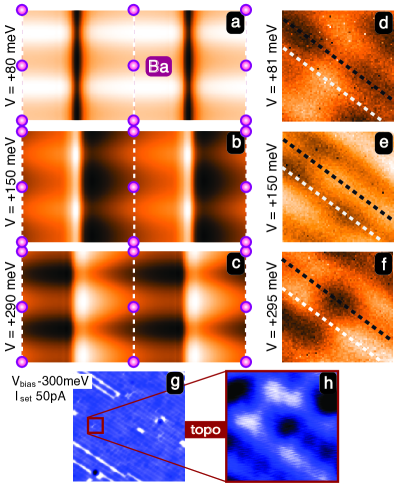
Going further than the three different lateral tip positions in Fig. 3, we now simulate tunneling conductance maps, constructed by varying the tip atom’s lateral position at a fixed distance from the surface of the slab (14 , as before). This generates a set of spectra as a function of tip position, which in this case are normalized such that the integral from meV is fixed. To create the conductance map for a particular bias voltage V, a slice through the simulated data-cube at this bias is then plotted as a function of .
Applying this procedure to the simulated data for the 1-reconstructed surface produces the maps shown in panels (a) - (c) of Fig. 4, for , , and meV, respectively. At meV, the 1 reconstruction is clearly seen in the calculated maps, appearing - for example - as a dark stripe joining the locations of the missing Ba atoms. Interestingly, as the bias voltage is increased to 150 meV (panel [b]) a clear contrast reversal takes place. This behavior in the model is confirmed in our measured tunneling conductance maps, shown in panels (d)-(f) of Fig. 4. These were measured with a 5 meV modulation on the bias voltage and had set-up parameters meV and pA, with normalization of the spectra to the area of the electron addition spectral weight up to 300 meV. The (black) white dashed lines in Fig. 4(d)-(f) are guides, marking the Ba adatom peaks (valleys) observed in the topography (panel [g]), of which a zoom is presented in Fig. 4(h). The measured maps show a similar relative contrast reversal at the same positive bias values. The peaks (valleys) in the conductance map at 80 meV (panel [d]) reverse roles at 150 meV, appearing instead as valleys (peaks) (panel [e]). If one traces along the occupied Ba row under the white dashed line in panel [e] at 150meV bias, the experiment indicates higher dI/dV between the positions of the Ba atoms (the latter visible in the topographic scan shown in panel [h] as bright features) and the corresponding theory map (panel [b]) shows the same behaviour. Moving up to a bias around 290meV in panel (c), a second type of contrast change occurs along the occupied Ba row where the occupied (unoccupied) Ba positions become brigher (darker). This change is also reflected in the experimental data (panel [f]). However, at 295 meV the agreement between theory and experiment is not perfect: theory predicts the highest intensity to occur in between the Ba rows whole in the experimental data the highest intensity occurs on the Ba rows. Nevertheless, the experimental confirmation of the contrast changes at lower bias voltage predicted by our DFT calculations closes the loop as regards the validity and precision of our theoretical description showing a heavily Ba-filtered tunneling current in STS of Co-doped Ba-122 superconductors.
In summary, our joint theoretical and experimental investigation has uncovered that the alkaline earth adatom termination layer in STS experiments on A-122 iron pnictide superconductors acts as a tunneling filter. Bands with strong Ba5d character in the Ba-122 system - which originate in the 1 reconstruction - are the door-keeper to a sub-set of the Fe3d related states from the uppermost Fe layer of the sub-surface As-Fe2-As block. Our model naturally explains the observed strong particle-hole asymmetry observed in the STS spectra, which cannot be found in the underlying Fe 3d partial DOS. We expect very similar adatom-filtering effects to impact the tunneling current in other alkaline-earth A-122 systems, but given the sensitivity to the surface reconstruction, experimental data regarding the real surface structure - such as those from LEED - are required before the different aspects can be successfully unravelled as we have done here.
Acknowledgements.
The authors acknowledge F. Massee, A. Kemper and A. V. Chubukov for useful discussions. This work was supported by the Foundation for Fundamental Research on Matter (FOM) and the VENI program (both part of of the Dutch NWO) and the EU (FP7/2007-2013, no. 226716).References
- (1) P. J. Hirschfeld, M. M. Korshunov, and I. I. Mazin, Rep. Prop. Phys. 74, 124508 (2011).
- (2) K. Terashima et al., PNAS 106, 7330 (2009).
- (3) A. Koitzsch et al., Phys. Rev. Lett. 102, 167001 2009.
- (4) M. Yi et al., PNAS 108, 6878 (2011).
- (5) E. van Heumen et al.,Phys. Rev. Lett 106, 027002 (2011).
- (6) J. E. Hoffman, Rep. Prog. Phys., 74, 124513 (2011).
- (7) F. Massee, S. de Jong, Y. Huang, J. Kaas, E. van Heumen, J. B. Goedkoop, and M. S. Golden, Phys. Rev. B 80, 140507(R) (2009).
- (8) F. Massee, Y. K. Huang, J. Kaas, E. van Heumen, S. de Jong, R. Huisman, H. Luigjes, J. B. Goedkoop, and M. S. Golden, Europhysics Lett. 92, 57012 (2010).
- (9) H. Zhang et al., Phys. Rev. B 81,104520 (2010).
- (10) Y. Yin, M. Zech, T. L. Williams, X. F. Wang, G. Wu, X. H. Chen, and J. E. Hoffman, Phys. Rev. Lett. 102, 097002 (2009).
- (11) T.-M. Chuang, M. P. Allan, J. Lee, Y. Xie, N. Ni,S. L. Bud’ko, G. S. Boebinger, P. C. Canfield, and J. C. Davis, Science 327, 181 (2010).
- (12) V. B. Nascimento et al., Phys. Rev. Lett. 103 076104 (2009).
- (13) M. Gao, F. Ma, Z.-Y. Lu, and T. Xiang, Phys. Rev. B 81, 193409 (2010).
- (14) T. Hanaguri et al., Nature (London) 430,1001 (2004)
- (15) J. Nieminen, H. Lin, R. S. Markiewicz, and A. Bansil, Phys. Rev. Lett. 102, 037001 (2009).
- (16) S. Graser, A. F. Kemper, T. A. Maier, H.-P. Cheng, P. J. Hirschfeld, and D. J. Scalapino, Phys. Rev. B 81, 214503 (2010).
- (17) See online supplementary material.
- (18) K. Koepernik, and H. Eschrig, Phys. Rev. B 59,1743 (1999); Version 9.09, http://www.fplo.de.
- (19) J. P. Perdew, and Y. Wang, Phys. Rev. B 45,13244(1992).
- (20) J. B. Pendry, A. B. Prêtre, and B. C. H. Krutzen, J.Phys.: Cond. Matt. 3, 4313 (1991).
- (21) K. Kobayashi and J. Yamauchi, Phys. Rev. B 51,17085 (1995).
- (22) I. Suominen et al., arXiv:1106.3302v1 (2011) unpublished.
- (23) J. Tersoff and D. R. Hamann, Phys. Rev. B 31,805 (1985).