Strong interaction studies with antiprotonsTechnical Design Report - MVD
Technical Design Report for the:
\Panda
Micro Vertex Detector
(AntiProton Annihilations at Darmstadt)
Strong Interaction Studies with Antiprotons
\Panda Collaboration
Technical Design Report for the:
\Panda
Micro Vertex Detector
(AntiProton Annihilations at Darmstadt)
Strong Interaction Studies with Antiprotons
\Panda Collaboration
30th November 2011
The \Panda Collaboration
\institemUniversität Basel, Switzerland
\authitemW. Erni,
\authitemI. Keshelashvili,
\authitemB. Krusche,
\authitemM. Steinacher\lastitem\institemInstitute of High Energy Physics, Chinese Academy of Sciences, Beijing, China
\authitemY. Heng,
\authitemZ. Liu,
\authitemH. Liu,
\authitemX. Shen,
\authitemQ. Wang,
\authitemH. Xu\lastitem\institemUniversität Bochum, I. Institut für Experimentalphysik, Germany
\authitemM. Albrecht,
\authitemJ. Becker,
\authitemK. Eickel,
\authitemF. Feldbauer,
\authitemM. Fink,
\authitemP. Friedel,
\authitemF.H. Heinsius,
\authitemT. Held,
\authitemH. Koch,
\authitemB. Kopf,
\authitemM. Leyhe,
\authitemC. Motzko,
\authitemM. Pelizäus,
\authitemJ. Pychy,
\authitemB. Roth,
\authitemT. Schröder,
\authitemJ. Schulze,
\authitemM. Steinke,
\authitemT. Trifterer,
\authitemU. Wiedner,
\authitemJ. Zhong\lastitem\institem Universität Bonn, Germany
\authitemR. Beck,
\authitemM. Becker,
\authitemS. Bianco,
\authitemK.-Th. Brinkmann,
\authitemC. Hammann,
\authitemF. Hinterberger,
\authitemR. Jäkel,
\authitemD. Kaiser,
\authitemR. Kliemt,
\authitemK. Koop,
\authitemC. Schmidt,
\authitemR. Schnell,
\authitemU. Thoma,
\authitemP. Vlasov,
\authitemC. Wendel,
\authitemA. Winnebeck,
\authitemTh. Würschig,
\authitemH.-G. Zaunick\lastitem\institemUniversità di Brescia, Brescia, Italy
\authitemA. Bianconi\lastitem\institemInstitutul National de C&D pentru Fizica si Inginerie Nucleara “Horia Hulubei”, Bukarest-Magurele, Romania
\authitemM. Bragadireanu,
\authitemM. Caprini,
\authitemM. Ciubancan,
\authitemD. Pantea,
\authitemP.-D Tarta\lastitem\institemDipartimento di Fisica e Astronomia dell’Università di Catania
and INFN, Sezione di Catania, Italy
\authitemM. De Napoli,
\authitemF. Giacoppo,
\authitemE. Rapisarda,
\authitemC. Sfienti\lastitem\institemAGH University of Science and Technology Cracow, Poland
\authitemT. Fiutowski,
\authitemN. Idzik,
\authitemB. Mindur,
\authitemD. Przyborowski,
\authitemK. Swientek\lastitem\institemIFJ, Institute of Nuclear Physics PAN, Cracow, Poland
\authitemE. Bialkowski,
\authitemA. Budzanowski,
\authitemB. Czech,
\authitemS. Kliczewski,
\authitemA. Kozela,
\authitemP. Kulessa,
\authitemP. Lebiedowicz,
\authitemK. Malgorzata,
\authitemK. Pysz,
\authitemW. Schäfer,
\authitemR. Siudak,
\authitemA. Szczurek\lastitem\institemInstitute of Applied Informatics, University of Technology, Cracow, Poland
\authitemP. Brandys,
\authitemT. Czyzewski,
\authitemW. Czyzycki,
\authitemM. Domagala,
\authitemM. Hawryluk,
\authitemG. Filo,
\authitemD. Kwiatkowski,
\authitemE. Lisowski,
\authitemF. Lisowski\lastitem\institemInstytut Fizyki, Uniwersytet Jagiellonski, Cracow, Poland
\authitemW. Bardan,
\authitemD. Gil,
\authitemB. Kamys,
\authitemSt. Kistryn,
\authitemK. Korcyl,
\authitemW. Krzemieñ,
\authitemA. Magiera,
\authitemP. Moskal,
\authitemZ. Rudy,
\authitemP. Salabura,
\authitemJ. Smyrski,
\authitemA. Wroñska\lastitem\institemGesellschaft für Schwerionenforschung mbH, Darmstadt, Germany
\authitemM. Al-Turany,
\authitemR. Arora,
\authitemI. Augustin,
\authitemH. Deppe,
\authitemD. Dutta,
\authitemH. Flemming,
\authitemK. Götzen,
\authitemG. Hohler,
\authitemR. Karabowicz,
\authitemD. Lehmann,
\authitemB. Lewandowski,
\authitemJ. Lühning,
\authitemF. Maas,
\authitemH. Orth,
\authitemK. Peters,
\authitemT. Saito,
\authitemG. Schepers,
\authitemC.J. Schmidt,
\authitemL. Schmitt,
\authitemC. Schwarz,
\authitemJ. Schwiening,
\authitemB. Voss,
\authitemP. Wieczorek,
\authitemA. Wilms\lastitem\institemVeksler-Baldin Laboratory of High Energies (VBLHE), Joint Institute for Nuclear Research. Dubna,
Russia
\authitemV.M. Abazov,
\authitemG.D. Alexeev,
\authitemV.A. Arefiev,
\authitemV.I. Astakhov,
\authitemM.Yu. Barabanov,
\authitemB.V. Batyunya,
\authitemYu.I. Davydov,
\authitemV.Kh. Dodokhov,
\authitemA.A. Efremov,
\authitemA.G. Fedunov,
\authitemA.A. Feshchenko,
\authitemA.S. Galoyan,
\authitemS. Grigoryan,
\authitemA. Karmokov,
\authitemE.K. Koshurnikov,
\authitemV.I. Lobanov,
\authitemYu.Yu. Lobanov,
\authitemA.F. Makarov,
\authitemL.V. Malinina,
\authitemV.L. Malyshev,
\authitemG.A. Mustafaev,
\authitemA.G. Olshevski,
\authitemM.A. Pasyuk,
\authitemE.A. Perevalova,
\authitemA.A. Piskun,
\authitemT.A. Pocheptsov,
\authitemG. Pontecorvo,
\authitemV.K. Rodionov,
\authitemYu.N. Rogov,
\authitemR.A. Salmin,
\authitemA.G. Samartsev,
\authitemM.G. Sapozhnikov,
\authitemG.S. Shabratova,
\authitemA.N. Skachkova,
\authitemN.B. Skachkov,
\authitemE.A. Strokovsky,
\authitemM.K. Suleimanov,
\authitemR.Sh. Teshev,
\authitemV.V. Tokmenin,
\authitemV.V. Uzhinsky
\authitemA.S. Vodopyanov,
\authitemS.A. Zaporozhets,
\authitemN.I. Zhuravlev,
\authitemA.G. Zorin\lastitem
\institemUniversity of Edinburgh, United Kingdom
\authitemD. Branford,
\authitemD. Glazier,
\authitemD. Watts,
\authitemP. Woods\lastitem\institemFriedrich Alexander Universität Erlangen-Nürnberg, Germany
\authitemA. Britting,
\authitemW. Eyrich,
\authitemA. Lehmann,
\authitemF. Uhlig\lastitem\institemNorthwestern University, Evanston, U.S.A.
\authitemS. Dobbs,
\authitemZ. Metreveli,
\authitemK. Seth,
\authitemB. Tann,
\authitemA. Tomaradze\lastitem\institemUniversità di Ferrara and INFN, Sezione di Ferrara, Italy
\authitemD. Bettoni,
\authitemV. Carassiti,
\authitemP. Dalpiaz,
\authitemA. Drago,
\authitemE. Fioravanti,
\authitemI. Garzia,
\authitemM. Negrini,
\authitemM. Savriè,
\authitemG. Stancari\lastitem\institemINFN-Laboratori Nazionali di Frascati, Italy
\authitemB. Dulach,
\authitemP. Gianotti,
\authitemC. Guaraldo,
\authitemV. Lucherini,
\authitemE. Pace\lastitem\institemINFN, Sezione di Genova, Italy
\authitemA. Bersani,
\authitemM. Macri,
\authitemM. Marinelli,
\authitemR.F. Parodi\lastitem\institemJustus Liebig-Universität Gießen, II. Physikalisches Institut, Germany
\authitemV. Dormenev,
\authitemP. Drexler,
\authitemM. Düren,
\authitemT. Eisner,
\authitemK. Foehl,
\authitemA. Hayrapetyan,
\authitemP. Koch,
\authitemB. Krïoch,
\authitemW. Kühn,
\authitemS. Lange,
\authitemY. Liang,
\authitemM. Liu,
\authitemO. Merle,
\authitemV. Metag,
\authitemM. Moritz,
\authitemM. Nanova,
\authitemR. Novotny,
\authitemB. Spruck,
\authitemH. Stenzel,
\authitemC. Strackbein,
\authitemM. Thiel,
\authitemQ. Wang
\lastitem\institemUniversity of Glasgow, United Kingdom
\authitemT. Clarkson,
\authitemC. Euan,
\authitemG. Hill,
\authitemM. Hoek,
\authitemD. Ireland,
\authitemR. Kaiser,
\authitemT. Keri,
\authitemI. Lehmann,
\authitemK. Livingston,
\authitemP. Lumsden,
\authitemD. MacGregor,
\authitemB. McKinnon,
\authitemR. Montgomery,
\authitemM. Murray,
\authitemD. Protopopescu,
\authitemG. Rosner,
\authitemB. Seitz,
\authitemG. Yang\lastitem\institemKernfysisch Versneller Instituut, University of Groningen, Netherlands
\authitemM. Babai,
\authitemA.K. Biegun,
\authitemA. Glazenborg-Kluttig,
\authitemE. Guliyev,
\authitemV.S. Jothi,
\authitemM. Kavatsyuk,
\authitemP. Lemmens,
\authitemH. Löhner,
\authitemJ. Messchendorp,
\authitemT. Poelman,
\authitemH. Smit,
\authitemJ.C. van der Weele\lastitem\institemFachhochschule Südwestfalen, Iserlohn, Germany
\authitemH. Sohlbach\lastitem\institemForschungszentrum Jülich, Institut für Kernphysik, Jülich, Germany
\authitemM. Büscher,
\authitemR. Dosdall,
\authitemR. Dzhygadlo,
\authitemS. Esch,
\authitemA. Gillitzer,
\authitemF. Goldenbaum,
\authitemD. Grunwald,
\authitemV. Jha,
\authitemG. Kemmerling,
\authitemH. Kleines,
\authitemA. Lehrach,
\authitemR. Maier,
\authitemM. Mertens,
\authitemH. Ohm,
\authitemD.L. Pohl,
\authitemD. Prasuhn,
\authitemT. Randriamalala,
\authitemJ. Ritman,
\authitemM. Roeder,
\authitemG. Sterzenbach,
\authitemT. Stockmanns,
\authitemP. Wintz,
\authitemP. Wüstner,
\authitemH. Xu\lastitem\institemUniversity of Silesia, Katowice, Poland
\authitemJ. Kisiel\lastitem\institemChinese Academy of Science, Institute of Modern Physics, Lanzhou, China
\authitemS. Li,
\authitemZ. Li,
\authitemZ. Sun,
\authitemH. Xu\lastitem\institemLunds Universitet, Department of Physics, Lund, Sweden
\authitemK. Fissum,
\authitemK. Hansen,
\authitemL. Isaksson,
\authitemM. Lundin,
\authitemB. Schröder\lastitem\institemJohannes Gutenberg-Universität, Institut für Kernphysik, Mainz, Germany
\authitemP. Achenbach,
\authitemA. Denig,
\authitemM. Distler,
\authitemM. Fritsch,
\authitemD. Kangh,
\authitemA. Karavdina,
\authitemW. Lauth,
\authitemM. Michel,
\authitemM.C. Mora Espi,
\authitemJ. Pochodzalla,
\authitemS. Sanchez,
\authitemA. Sanchez-Lorente,
\authitemC. Sfienti,
\authitemT. Weber\lastitem\institemResearch Institute for Nuclear Problems, Belarus State University, Minsk, Belarus
\authitemV.I. Dormenev,
\authitemA.A. Fedorov,
\authitemM.V. Korzhik,
\authitemO.V. Missevitch\lastitem\institemInstitute for Theoretical and Experimental Physics, Moscow, Russia
\authitemV. Balanutsa,
\authitemV. Chernetsky,
\authitemA. Demekhin,
\authitemA. Dolgolenko,
\authitemP. Fedorets,
\authitemA. Gerasimov,
\authitemV. Goryachev\lastitem\institemMoscow Power Engineering Institute, Moscow, Russia
\authitemA. Boukharov,
\authitemO. Malyshev,
\authitemI. Marishev,
\authitemA. Semenov\lastitem\institemIIT Bombay, Department of Physics, Mumbai, India
\authitemR. Varma\lastitem
\institemTechnische Universität München, Germany
\authitemB. Ketzer,
\authitemI. Konorov,
\authitemA. Mann,
\authitemS. Neubert,
\authitemS. Paul,
\authitemM. Vandenbroucke,
\authitemQ. Zhang\lastitem\institemWestfälische Wilhelms-Universität Münster, Germany
\authitemA. Khoukaz,
\authitemT. Rausmann,
\authitemA. Täschner,
\authitemJ. Wessels\lastitem\institemBudker Institute of Nuclear Physics, Novosibirsk, Russia
\authitemE. Baldin,
\authitemK. Kotov,
\authitemS. Peleganchuk,
\authitemYu. Tikhonov\lastitem\institemInstitut de Physique Nucléaire, Orsay, France
\authitemT. Hennino,
\authitemM. Imre,
\authitemR. Kunne,
\authitemC. Le Galliard,
\authitemJ.P. Le Normand,
\authitemD. Marchand,
\authitemA. Maroni,
\authitemS. Ong,
\authitemJ. Pouthas,
\authitemB. Ramstein,
\authitemP. Rosier,
\authitemM. Sudol,
\authitemC. Theneau,
\authitemE. Tomasi-Gustafsson,
\authitemJ. Van de Wiele,
\authitemT. Zerguerras\lastitem\institemDipartimento di Fisica Nucleare e Teorica, Università di Pavia,
INFN, Sezione di Pavia, Pavia, Italy
\authitemG. Boca,
\authitemA. Braghieri,
\authitemS. Costanza,
\authitemA. Fontana,
\authitemP. Genova,
\authitemL. Lavezzi,
\authitemP. Montagna,
\authitemA. Rotondi\lastitem\institemInstitute for High Energy Physics, Protvino, Russia
\authitemV. Buda,
\authitemV.V. Abramov,
\authitemA.M. Davidenko,
\authitemA.A. Derevschikov,
\authitemY.M. Goncharenko,
\authitemV.N. Grishin,
\authitemV.A. Kachanov,
\authitemD.A. Konstantinov,
\authitemV.A. Kormilitsin,
\authitemY.A. Matulenko,
\authitemY.M. Melnik
\authitemA.P. Meschanin,
\authitemN.G. Minaev,
\authitemV.V. Mochalov,
\authitemD.A. Morozov,
\authitemL.V. Nogach,
\authitemS.B. Nurushev,
\authitemA.V. Ryazantsev,
\authitemP.A. Semenov,
\authitemL.F. Soloviev,
\authitemA.V. Uzunian,
\authitemA.N. Vasiliev,
\authitemA.E. Yakutin\lastitem\institemPetersburg Nuclear Physics Institute of Academy of Science,
Gatchina, St. Petersburg, Russia
\authitemS. Belostotski,
\authitemG. Gavrilov,
\authitemA. Itzotov,
\authitemA. Kisselev,
\authitemP. Kravchenko,
\authitemS. Manaenkov,
\authitemO. Miklukho,
\authitemY. Naryshkin,
\authitemD. Veretennikov,
\authitemV. Vikhrov,
\authitemA. Zhadanov\lastitem\institemKungliga Tekniska Högskolan, Stockholm, Sweden
\authitemT. Bäck,
\authitemB. Cederwall\lastitem\institemStockholms Universitet, Stockholm, Sweden
\authitemC. Bargholtz,
\authitemL. Gerén,
\authitemP.E. Tegnér,
\authitemP. Thørngren,
\authitemK.M. von Würtemberg\lastitem\institemUniversità del Piemonte Orientale Alessandria
and INFN, Sezione di Torino, Torino, Italy
\authitemL. Fava\lastitem\institemUniversità di Torino and INFN, Sezione di Torino, Torino, Italy
\authitemD. Alberto,
\authitemA. Amoroso,
\authitemM.P. Bussa,
\authitemL. Busso,
\authitemF. De Mori,
\authitemM. Destefanis,
\authitemL. Ferrero,
\authitemM. Greco,
\authitemT. Kugathasan,
\authitemM. Maggiora,
\authitemS. Marcello,
\authitemS. Sosio,
\authitemS. Spataro\lastitem\institemINFN, Sezione di Torino, Torino, Italy
\authitemD. Calvo,
\authitemS. Coli,
\authitemP. De Remigis,
\authitemA. Filippi,
\authitemG. Giraudo,
\authitemS. Lusso,
\authitemG. Mazza,
\authitemM. Mignone,
\authitemA. Rivetti,
\authitemR. Wheadon,
\authitemL. Zotti\lastitem\institemINAF-IFSI and INFN, Sezione di Torino, Torino, Italy
\authitemO. Morra\lastitem\institemPolitecnico di Torino and INFN, Sezione di Torino, Torino, Italy
\authitemF. Iazzi,
\authitemA. Lavagno,
\authitemP. Quarati,
\authitemK. Szymanska\lastitem\institemUniversità di Trieste and INFN, Sezione di Trieste, Trieste, Italy
\authitemR. Birsa,
\authitemF. Bradamante,
\authitemA. Bressan,
\authitemA. Martin\lastitem\institemUniversität Tübingen, Tübingen, Germany
\authitemH. Clement\lastitem\institemThe Svedberg Laboratory, Uppsala, Sweden
\authitemB. Galnander\lastitem\institemUppsala Universitet, Institutionen för Strålningsvetenskap, Uppsala, Sweden
\authitemH. Calén,
\authitemK. Fransson,
\authitemT. Johansson,
\authitemA. Kupsc,
\authitemP. Marciniewski,
\authitemE. Thomé,
\authitemM. Wolke,
\authitemJ. Zlomanczuk\lastitem\institemUniversitat de Valencia, Dpto. de Física Atómica, Molecular y Nuclear, Valencia, Spain
\authitemJ. Díaz,
\authitemA. Ortiz\lastitem\institemWarsaw University of Technology, Institute of Atomic Energy Otwock-Swierk, Warsaw, Poland
\authitemP. Buda,
\authitemK. Dmowski,
\authitemR. Korzeniewski,
\authitemD. Przemyslaw,
\authitemB. Slowinski\lastitem\institemSoltan Institute for Nuclear Studies, Warsaw, Poland
\authitemS. Borsuk,
\authitemA. Chlopik,
\authitemZ. Guzik,
\authitemJ. Kopec,
\authitemT. Kozlowski,
\authitemD. Melnychuk,
\authitemM. Plominski,
\authitemJ. Szewinski,
\authitemK. Traczyk,
\authitemB. Zwieglinski\lastitem\institemÖsterreichische Akademie der Wissenschaften, Stefan Meyer Institut für Subatomare Physik, Wien, Austria
\authitemP. Bühler,
\authitemA. Gruber,
\authitemP. Kienle,
\authitemJ. Marton,
\authitemE. Widmann,
\authitemJ. Zmeskal\lastitem
| Editors: | K.-Th. Brinkmann | Email: Brinkmann@hiskp.uni-bonn.de |
| D. Calvo | Email: calvo@to.infn.it |
|
| T. Stockmanns | Email: t.stockmanns@fz-juelich.de |
|
| Technical Coordinator: | Lars Schmitt | Email: l.schmitt@gsi.de
|
| Deputy: | Bernd Lewandowski | Email: b.lewandowski@gsi.de
|
| Spokesperson: | Ulrich Wiedner | Email: ulrich.wiedner@ruhr-uni-bochum.de
|
| Deputy: | Paola Gianotti | Email: paola.gianotti@lnf.infn.it |
MVD Group:
| L. Ackermann2 | H. Kleines6 | M. Ramm6 |
| M. Becker1 | R. Kliemt1 | O. Reinecke2 |
| S. Bianco1 | K. Koop1 | J. Ritman4 |
| K.-Th. Brinkmann1 | M. Kosmata2 | A. Rivetti8 |
| L. Busso9 | F. Krüger2 | R. Schnell1 |
| D. Calvo8 | T. Kugathasan9 | H. Sohlbach3 |
| S. Coli8 | S. Marcello9 | T. Stockmanns4 |
| F. De Mori9 | G. Mazza8 | J. Tummo1 |
| P. De Remigis8 | M. Mertens4 | P. Vlasov1 |
| D. Deermann4 | M. Mignone8 | R. Wheadon8 |
| S. Esch4 | O. Morra7 | Th. Würschig1 |
| A. Filippi8 | J. Pfennings5 | P. Wüstner6 |
| G. Giraudo8 | R. Pietzsch2 | H.-G. Zaunick1 |
| D. Grunwald5 | A. Pitka1 | L. Zotti9 |
| R. Jäkel2 | D.-L. Pohl4 | |
| V. Jha4 | T. Quagli9 |
1 HISKP, Universität Bonn, Germany
2 IKTP, TU Dresden, Germany
3 FH Südwestfalen, Fachbereich Informatik und Naturwissenschaften, Iserlohn, Germany
4 Forschungszentrum Jülich, Institut für Kernphysik, Jülich, Germany
5 ZAT, Jülich, Germany
6 ZEL, Jülich, Germany
7 INAF-IFSI and INFN, Sezione di Torino, Torino, Italy
8 INFN, Sezione di Torino, Torino, Italy
9 Università di Torino and INFN, Sezione di Torino, Torino, Italy
Preface
This document illustrates the technical layout and the expected performance
of the Micro Vertex Detector (MVD) of the \Pandaexperiment. The MVD will
detect charged particles as close as possible to the interaction zone.
Design criteria and the optimisation process as well as the technical
solutions chosen are discussed and the results of this process are
subjected to extensive Monte Carlo physics studies. The route towards
realisation of the detector is outlined.
The use of registered names, trademarks, \etcin this publication does not imply, even in the absence of specific statement, that such names are exempt from the relevant laws and regulations and therefore free for general use.
Chapter 1 The \PandaExperiment and its Tracking Concept
The following sections contain a general introduction to the \Pandaexperiment and, in particular, a short description of the implemented overall tracking concept. They belong to a common introductory part for the volumes of all individual tracking systems.
1.1 The \PandaExperiment
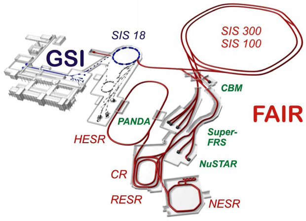
The \Panda(AntiProton ANnihilation at DArmstadt) experiment [PANDA-LOI] is one of the key projects at the future Facility for Antiproton and Ion Research (\Fair) [FAIR1] [Greenpaper], which is currently under construction at GSI, Darmstadt. For this new facility the present GSI accelerators will be upgraded and further used as injectors. The completed accelerator facility will feature a complex structure of new accelerators and storage rings. An overview of the \Fairfacility is given in figure 1.1. Further details of the accelerator complex are described in [FAIR-Accelerator]. The \Fairaccelerators will deliver primary proton and ion beams as well as secondary beams of antiprotons or radioactive ions, all with high energy, high intensity and high quality. Experiments to be installed at the facility will address a wide range of physics topics in the fields of nuclear and hadron physics as well as in atomic and plasma physics. An executive summary of the main \Fairprojects can be found in [FAIR1] and [FAIR2].
The \Pandaexperiment will perform precise studies of antiproton-proton annihilations and reactions of antiprotons with nucleons of heavier nuclear targets. It will benefit from antiproton beams with unprecedented intensity and quality. The covered centre-of-mass energy between 1 \gevand 5 \gevallows for very accurate measurements, especially in the charm quark sector. Based on a broad physics program, studying the non-pertubative regime, it will be possible to explore the nature of the strong interaction and to obtain a significant progress in our understanding of the QCD spectrum and hadron structure.
Nowadays these studies are carried out mainly at electron machines that offer the advantage of kinematically clean reactions but at the price of a reduced set of final states and reduced cross-sections. Also the future experiments currently planned as upgrade at existing high-energy physics facilities will not deliver high-precision data over the full charm spectrum. In this context, the \Pandaexperiment will be a unique tool to improve both statistics and precision of existing data and to further explore the physics in the charm quark sector. Moreover, the \Pandacollaboration is in the ideal situation to be able to benefit from the expertise gained during the construction of the LHC detectors and of the B-factory experiments, which have determined a significant progress in the detector technology due to the performed optimisation or the introduction of completely new concepts and instruments.
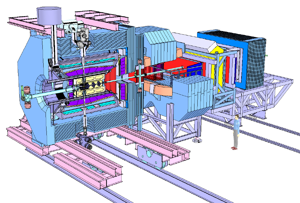
In the first section of this chapter the scientific program of \Pandawill be summarised. It ranges from charmonium spectroscopy to the search for exotic hadrons and the study of nucleon structure, from the study of in-medium modifications of hadron masses to the physics of hypernuclei. Therefore, antiproton beams in the momentum range from 1.5 \gevcto 15 \gevcwill be provided by the high-energy storage ring (\HESR) to the experiment. An overview of this accelerator and storage ring will be given in the second section. To explore the broad physics program, the \Pandacollaboration wants to build a state-of-the-art general purpose detector studying annihilation reactions of antiprotons with protons (\pbarp) and in nuclear matter (\pbarA). The different target systems will be discussed in section 1.1.3. The \Pandaapparatus consists of a set of systems surrounding an internal target placed in one of the two straight sections of the \HESR. Figure 1.2 shows the layout of the \Pandadetector. It consists of a 4 m long and 2 T strong superconducting solenoid instrumented to detect both charged and neutral particles emitted at large and backward angles (Target Spectrometer, TS) and of a 2 Tm resistive dipole magnetic spectrometer to detect charged and neutral particles emitted at angles between zero and twenty degrees (Forward Spectrometer, FS) with respect to the beam axis. A complex detector arrangement is necessary in order to reconstruct the complete set of final states, relevant to achieve the proposed physics goals. With the installed setup, a good particle identification with an almost complete solid angle will be combined with excellent mass, momentum and spatial resolution. More details of the \Pandadetector will be described in section 1.2.
1.1.1 The Scientific Program
One of the most challenging and fascinating goals of modern physics is the achievement of a fully quantitative understanding of the strong interaction, which is the subject of hadron physics. Significant progress has been achieved over the past few years thanks to considerable advances in experiment and theory. New experimental results have stimulated a very intense theoretical activity and a refinement of the theoretical tools.
Still there are many fundamental questions which remain basically unanswered. Phenomena such as the confinement of quarks, the existence of glueballs and hybrids, the origin of the masses of hadrons in the context of the breaking of chiral symmetry are long-standing puzzles and represent the intellectual challenge in our attempt to understand the nature of the strong interaction and of hadronic matter.
Experimentally, studies of hadron structure can be performed with different probes such as electrons, pions, kaons, protons or antiprotons. In antiproton-proton annihilation, particles with gluonic degrees of freedom as well as particle-antiparticle pairs are copiously produced, allowing spectroscopic studies with very high statistics and precision. Therefore, antiprotons are an excellent tool to address the open problems.
The \PANDAexperiment is being designed to fully exploit the extraordinary physics potential arising from the availability of high-intensity, cooled antiproton beams. Main experiments of the rich and diversified hadron physics program are briefly itemised in the following. More details can be found in the \pandaphysics booklet [PANDA:PhysBooklet].
-
•
Charmonium Spectroscopy
A precise measurement of all states below and above the open charm threshold is of fundamental importance for a better understanding of QCD. All charmonium states can be formed directly in \pbarpannihilation. At full luminosity \PANDAwill be able to collect several thousand \ccbarstates per day. By means of fine scans it will be possible to measure masses with accuracies of the order of 100 \kevand widths to 10% or better. The entire energy region below and above the open charm threshold will be explored. -
•
Search for Gluonic Excitations
One of the main challenges of hadron physics is the search for gluonic excitations, i.e. hadrons in which the gluons can act as principal components. These gluonic hadrons fall into two main categories: glueballs, i.e. states of pure glue, and hybrids, which consist of a \qqbarpair and excited glue. The additional degrees of freedom carried by gluons allow these hybrids and glueballs to have \JPCexotic quantum numbers: in this case mixing effects with nearby \qqbarstates are excluded and this makes their experimental identification easier. The properties of glueballs and hybrids are determined by the long-distance features of QCD and their study will yield fundamental insight into the structure of the QCD vacuum. Antiproton-proton annihilations provide a very favourable environment in which to look for gluonic hadrons. -
•
Study of Hadrons in Nuclear Matter
The study of medium modifications of hadrons embedded in hadronic matter is aiming at understanding the origin of hadron masses in the context of spontaneous chiral symmetry breaking in QCD and its partial restoration in a hadronic environment. So far experiments have been focussed on the light quark sector. The high-intensity \pbarbeam of up to 15 \gevcwill allow an extension of this program to the charm sector both for hadrons with hidden and open charm. The in-medium masses of these states are expected to be affected primarily by the gluon condensate.Another study which can be carried out in \PANDAis the measurement of \jpsiand \Dmeson production cross sections in \pbarannihilation on a series of nuclear targets. The comparison of the resonant \jpsiyield obtained from \pbarannihilation on protons and different nuclear targets allows to deduce the \jpsi-nucleus dissociation cross section, a fundamental parameter to understand \jpsisuppression in relativistic heavy ion collisions interpreted as a signal for quark-gluon plasma formation.
-
•
Open Charm Spectroscopy
The \HESR, running at full luminosity and at \pbarmomenta larger than 6.4 \gevc, would produce a large number of \Dmeson pairs. The high yield and the well defined production kinematics of \Dmeson pairs would allow to carry out a significant charmed meson spectroscopy program which would include, for example, the rich \Dand \Dsmeson spectra. -
•
Hypernuclear Physics
Hypernuclei are systems in which neutrons or protons are replaced by hyperons. In this way a new quantum number, strangeness, is introduced into the nucleus. Although single and double \Lambdaplain-hypernuclei were discovered many decades ago, only 6 double \Lambdaplain-hypernuclei are presently known. The availability of \pbarbeams at \FAIRwill allow efficient production of hypernuclei with more than one strange hadron, making \PANDAcompetitive with planned dedicated facilities. This will open new perspectives for nuclear structure spectroscopy and for studying the forces between hyperons and nucleons. -
•
Electromagnetic Processes
In addition to the spectroscopic studies described above, \PANDAwill be able to investigate the structure of the nucleon using electromagnetic processes, such as Deeply Virtual Compton Scattering (DVCS) and the process \pbarp \ee, which will allow the determination of the electromagnetic form factors of the proton in the timelike region over an extended region. Furthermore, measuring the Drell Yan production of muons would give access to the transverse nucelon structure.
1.1.2 High Energy Storage Ring – \HESR
| Experimental Requirements | |
|---|---|
| Ion species | Antiprotons |
| production rate | /s ( per 10 min) |
| Momentum / Kinetic energy range | 1.5 to 15 \gevc/ 0.83 to 14.1 \gev |
| Number of particles | to |
| Betatron amplitude at IP | 1 m to 15 m |
| Betatron amplitude E-Cooler | 25 m to 200 m |
| Operation Modes | |
| High resolution (HR) | Peak Luminosity of 2cm-2s-1 for |
| assuming = atoms/cm2 | |
| RMS momentum spread , | |
| 1.5 to 8.9 \gevc | |
| High luminosity (HL) | Peak Luminosity up to 2cm-2s-1 for |
| assuming = atoms/cm2 | |
| RMS momentum spread , | |
| 1.5 to 15 \gevc | |
The \HESRis dedicated to supply \PANDAwith high intensity and high quality antiproton beams over a broad momentum range from 1.5 \gevcto 15 \gevc [HESR:FAIR:2008]. Table 1.1 summarises the experimental requirements and main parameters of the two operation modes for the full \Fairversion. The High Luminosity (HL) and the High Resolution (HR) mode are established to fulfil all challenging specifications for the experimental program of \PANDA [hesr:lehrach:2009]. The HR mode is defined in the momentum range from 1.5 \gevcto 9 \gevc. To reach a relative momentum spread down to the order of , only circulating particles in the ring are anticipated. The HL mode requires an order of magnitude higher beam intensity with reduced momentum resolution to reach a peak luminosity of 2cm-2s-1 in the full momentum range up to 15 \gevc. To reach these beam parameters a very powerful phase-space cooling is needed. Therefore, high-energy electron cooling [Ecool08] and high-bandwidth stochastic cooling [HESR-CoolingScenario] will be utilised.
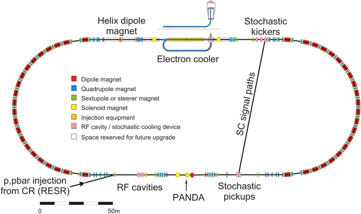
The \HESRlattice is designed as a racetrack shaped ring with a maximum beam rigidity of 50 Tm (see figure 1.3). It consists of two 180∘ arcs and two 155 m long straight sections with a total circumference of 575 m [HESR-Lattice]. The arc quadrupole magnets will allow for a flexible adjustment of transition energy, horizontal and vertical betatron tune as well as horizontal dispersion. In the straight section opposite to the injection point, an electron cooler will be installed. The \pandadetector with the internal target is placed at the other side. Further components in the straight \pandasection are beam injection kickers, septa and multi-harmonic RF cavities. The latter allow for a compensation of energy losses due to the beam-target interaction, a bunch rotation and the decelerating or accelerating of the beam. Stochastic cooling is implemented via several kickers and opposing high-sensitivity pick-ups on either side of the straight sections.
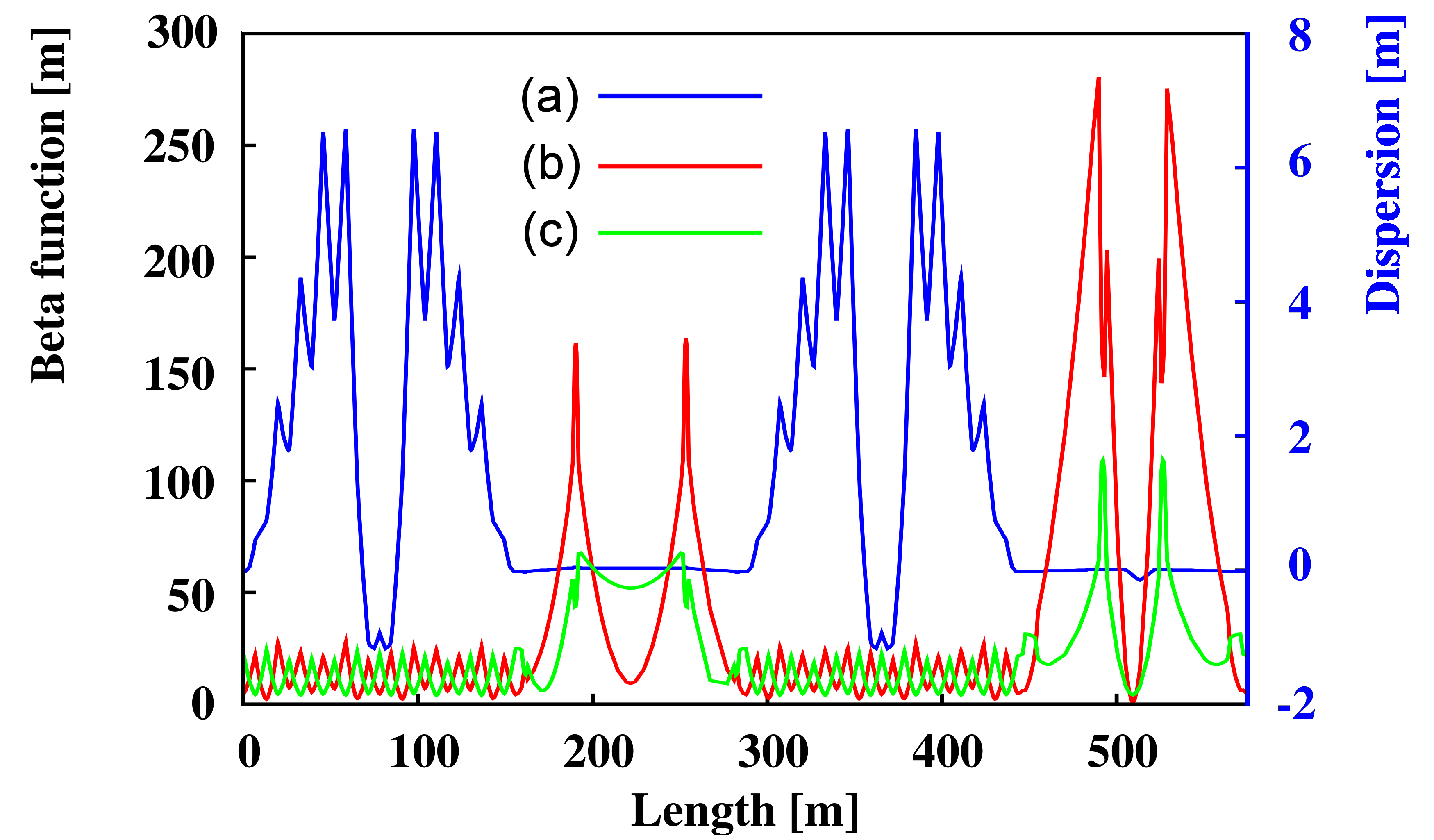
Special requirements for the lattice are low dispersion in the straight sections and small betatron amplitudes in the range between 1 m and 15 m at the internal interaction point (IP) of the \PANDAdetector. In addition, the betatron amplitude at the electron cooler must be adjustable within a large range between 25 m and 200 m. Examples of the optical functions for one of the defined optical settings are shown in figure 1.4. The deflection of the spectrometer dipole magnet of the \Pandadetector will be compensated by two dipole magnets that create a beam chicane. These will be placed 4.6 m upstream and 13 m downstream the \PandaIP thus defining a boundary condition for the quadrupole elements closest to the experiment. For symmetry reasons, they have to be placed at 14 m with respect to the IP. The asymmetric placement of the chicane dipoles will result in the experiment axis occurring at a small angle with respect to the axis of the straight section. The \PANDAsolenoid will be compensated by one solenoid magnet. Additional correction dipoles have to be included around the electron cooler due to the toroids that will be used to overlap the electron beam with the antiproton beam. Phase-space coupling induced by the electron cooler solenoid will be compensated by two additional solenoid magnets.
Closed orbit correction and local orbit bumps at dedicated locations in the ring are crucial to meet requirements for the beam-target interaction in terms of maximised ring acceptance and optimum beam-target overlap [Wel08]. The envisaged scheme aims on a reduction of maximum closed orbit deviations to below 5 mm while not exceeding 1 mrad of corrector strength. Therefore, 64 beam position monitors and 48 orbit correction dipoles are intended to be used. Because a few orbit bumps will have to be used in the straight parts of the \HESR, all correction dipoles therein are designed to provide an additional deflection strength of 1 mrad.
Transverse and longitudinal cooling will be used to compensate a transverse beam blow up and to achieve a low momentum spread, respectively. While stochastic cooling will be applicable in the whole momentum range, electron cooling is foreseen in a range from 1.5 \gevcto 8.9 \gevcwith a possible upgrade to 15 \gevc. The relative momentum spread can be further improved by combining both cooling systems. Beam losses are dominated by hadronic interactions between antiprotons and target protons, single large-angle Coulomb scattering in the target and energy straggling induced by Coulomb interactions of the antiprotons with target electrons. Mean beam lifetimes for the \HESRrange between 1540 s and 7100 s. The given numbers correspond to the time, after which the initial beam intensity is reduced by a factor of . A detailed discussion of the beam dynamics and beam equliibria for the \HESRcan be found in [hesr:lehrach:2009, lehrach:2006, hinterberger:2006, BoineFrankenheim:2006ci]. Advanced simulations have been performed for both cooling scenarios. In case of electron cooled beams the RMS relative momentum spread obtained for the HR mode ranges from (1.5 \gevc) to (8.9 \gevc), and (15 \gevc) [Rei07]. With stochastic cooling in a bandwidth of 2 GHz to 6 GHz, the RMS relative momentum spread for the HR mode results in (3.8 \gevc), (8.9 \gevc) and (15 \gevc) [Sto08]. In the HL mode a RMS relative momentum spread of roughly can be expected. Transverse stochastic cooling can be adjusted independently to ensure sufficient beam-target overlap.

1.1.3 Targets
The design of the solenoid magnet allows for an implementation of different target systems. \pandawill use both gaseous and non-gaseous targets. A very precise positioning of the target is crucial for the exact definition of the primary interaction vertex. In this context, big challenges for either system result from the long distance of roughly 2 m between the target injection point and the dumping system. Hydrogen target systems will be used for the study of antiproton-proton reactions. A high effective target density of about hydrogen atoms per square centimetre must be achieved to fulfill the design goals of the high luminosity mode. Besides the application of hydrogen as target material, an extension to heavier gases such as deuterium, nitrogen or argon is planned for complementary studies with nuclear targets.
At present, two different solutions are under development: a cluster-jet and a pellet target. Both will potentially provide sufficient target thickness but exhibit different properties concerning their effect on the beam quality and the definition of the IP. Solid targets are foreseen for hyper-nuclear studies and the study of antiproton-nucleus interaction using heavier nuclear targets. The different target options are shortly described in the following. Figure 1.5 gives an overview to all target option foreseen at \panda.
Cluster Jet Target
Cluster jet targets provide a homogeneous and adjustable target density without any time structure. Optimum beam conditions can be applied in order to achieve highest luminosity. The uncertainty of the IP in a plane perpendicular to the beam axis is defined by the optimised focus of the beam only. An inherent disadvantage of cluster-jet targets is the lateral spread of the cluster jet leading to an uncertainty in the definition of the IP along the beam axis of several millimetres.
For the target production a pressurised cooled gas is injected into vacuum through a nozzle. The ejected gas immediately condensates and forms a narrow supersonic jet of molecule clusters. The cluster beam typically exposes a broad mass distribution which strongly depends on the gas input pressure and temperature. In case of hydrogen, the average number of molecules per cluster varies from 103 to 106. The cluster-jets represent a highly diluted target and offer a very homogenous density profile. Therefore, they may be seen as a localised and homogeneous monolayer of hydrogen atoms being passed by the antiprotons once per revolution, i.e. the antiproton beam can be focused at highest phase space density. The interaction point is thus defined transversely but has to be reconstructed longitudinally in beam direction. At a dedicated prototype cluster target station an effective target density of hydrogen atoms per square centimetre has been achieved using the exact \pandageometry [taeschner:2011]. This value is close to the maximum number required by \panda. Even higher target densities seem to be feasible and are topic of ongoing R&D work.
Hydrogen Pellet Target
Pellet targets provide a stream of frozen molecule droplets, called pellets, which drip with a fixed frequency off from a fine nozzle into vacuum. The use of pellet targets gives access to high effective target densities. The spatial resolution of the interaction zone can be reduced by skimmers to a few millimetres. A further improvement of this resolution can be achieved by tracking the individual pellets. However, pellet targets suffer from a non-uniform time distribution, which results in larger variations of the instantaneous luminosity as compared to a cluster-jet target. The maximum achievable average luminosity is very sensitive to deviations of individual pellets from the target axis. The beam must be widened in order to warrant a beam crossing of all pellets. Therefore, an optimisation between the maximum pellet-beam crossing time on the one hand and the beam focusing on the other is necessary.
The design of the planned pellet target is based on the one currently used at the WASA-at-COSY experiment [WASA-Pellet]. The specified design goals for the pellet size and the mean lateral spread of the pellet train are given by a radius of 25 m to 40 m and a lateral RMS deviation in the pellet train of approximately 1 mm, respectively. At present, typical variations of the interspacing of individual pellets range between 0.5 mm and 5 mm. A new test setup with an improved performance has been constructed [PANDA-PelletTarget]. First results have demonstrated the mono-disperse and satellite-free droplet production for cryogenic liquids of H2, N2 and Ar [PANDA-PelletTarget2009]. However, the prototype does not fully include the \pandageometry. The handling of the pellet train over a long distance still has to be investigated in detail. The final resolution on the interaction point is envisaged to be in the order of 50 m. Therefore, an additional pellet tracking system is planned.
Other Target Options
In case of solid target materials the use of wire targets is planned. The hyper-nuclear program requires a separate target station in upstream position. It will comprise a primary and secondary target. The latter must be instrumented with appropriate detectors. Therefore, a re-design of the innermost part of the \pandaspectrometer becomes necessary. This also includes the replacement of the MVD.
1.1.4 Luminosity Considerations
The luminosity describes the flux of beam particles convolved with the target opacity. Hence, an intense beam, a highly effective target thickness and an optimised beam-target overlap are essential to yield a high luminosity in the experiment. The product of and the total hadronic cross section delivers the interaction rate , i.e. the number of antiproton-proton interactions in a specified time interval, which determines the achievable number of events for all physics channels and allows the extraction of occupancies in different detector regions. These are needed as input for the associated hardware development.
Obviously, the achievable luminosity is directly linked with the number of antiprotons in the \HESR. The particles are injected at discrete time intervals. The maximum luminosity thus depends on the antiproton production rate = d/d. Moreover, a beam preparation must be performed before the target can be switched on. It includes pre-cooling to equilibrium, the ramping to the desired beam momentum and a fine-tuned focusing in the target region as well as in the section for the electron cooler. Therefore, the operation cycle of the \HESRcan be separated into two sequences related to the beam preparation time (target off) and the time for data taking (target on), respectively. The beam preparation time also contains the period between the target switch-off and the injection, at which the residual antiprotons are either dumped or transferred back to the injection momentum.
Macroscopic Luminosity Profile
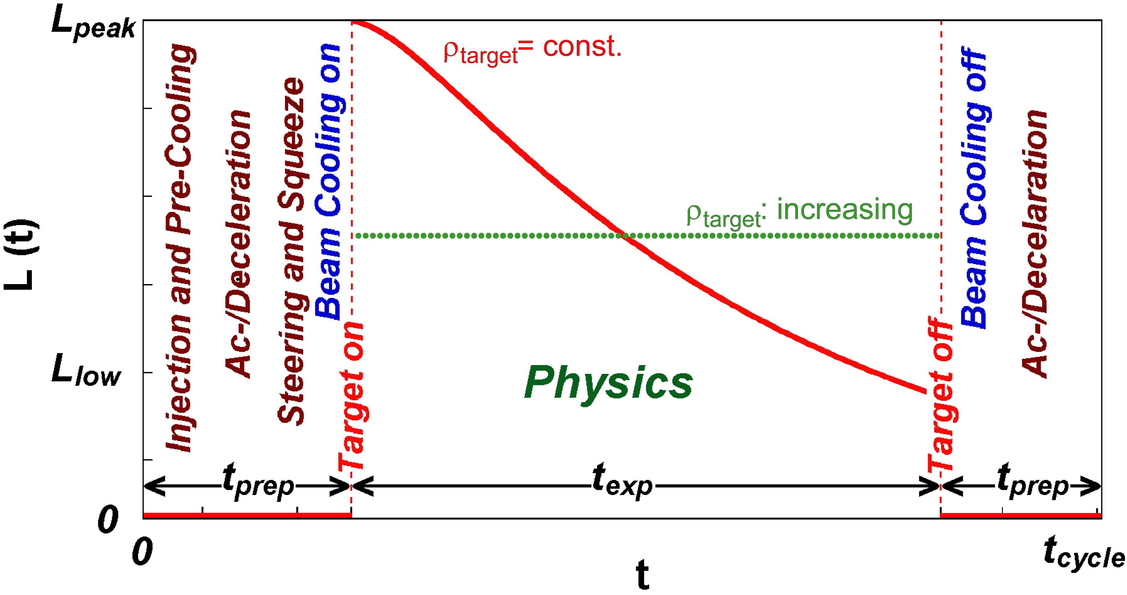
A schematic illustration of the luminosity profile during one operation cycle is given in figure 1.6. The maximum luminosity is obtained directly after the target is switched on. During data taking the luminosity decreases due to hadronic interactions, single Coulomb scattering and energy straggling of the circulating beam in the target. Compared to beam-target interaction, minor contributions are related to single intra-beam scattering (Touschek effect). Beam losses caused by residual gas scattering can be neglected, if the vacuum is better than 10-9 mbar. A detailed analysis of all beam loss processes can be found in [lehrach:2006, hinterberger:2006]. The relative beam loss rate for the total cross section is given by the expression
| (1.1) |
where corresponds to the mean (1/) beam lifetime, is the revolution frequency of the antiprotons in the ring and is the effective target thickness defined as an area density given in atoms per square centimetre. For beam-target interactions, the beam lifetime is independent of the beam intensity. The Touschek effect depends on the beam equilibria and beam intensity. At low momenta the beam cooling scenario and the ring acceptance have large impact on the achievable beam lifetime.
| 1.5 \gevc | 9 \gevc | 15 \gevc | |
| Total hadronic cross section/ mbarn | |||
| Cluster jet target | |||
| Target density: /cm-2 | |||
| Antiproton production rate: /s-1 | |||
| Beam preparation time: /s | |||
| Optimum cycle duration: /s | |||
| Mean beam lifetime: /s | |||
| Max Cycle Averaged Luminosity: /cm-2s-1 | |||
| Pellet target | |||
| Target density: / cm-2 | |||
| Antiproton production rate: /s-1 | |||
| Beam preparation time: /s | |||
| Optimum cycle duration: /s | |||
| Mean beam lifetime: /s | |||
| Max Cycle Averaged Luminosity: /cm-2s-1 | |||
Cycle Average Luminosity
| Target material | (=1.5 \gevc) | (=15 \gevc) | |
|---|---|---|---|
| [cm-2s-1] | [cm-2s-1] | [atoms/cm2] | |
| deuterium | |||
| argon | |||
| gold |
In physics terms, the time-averaged cycle luminosity is most relevant. The maximum average luminosity depends on the ratio of the antiproton production rate to the loss rate and is thus inversely proportional to the total cross section. It can be increased if the residual antiprotons after each cycle are transferred back to the injection momentum and then merged with the newly injected particles. Therefore, a bucket scheme utilising broad-band cavities is foreseen for beam injection and the refill procedure. Basically, the cycle average luminosity reads as:
| (1.2) |
where corresponds to the number of available particles at the start of the target insertion.
For the calculations, machine cycles and beam preparation times have to be specified. The maximum cycle average luminosity is achieved by an optimisation of the cycle time . Constraints are given by the restricted number antiprotons in the \HESR, the achievable effective target thickness and the specified antiproton production rate of s-1 at \FAIR.
Main results of calculations performed for different hydrogen targets are summarised in table 1.2. The total hadronic cross section, , decreases with higher beam momentum from approximately 100 mbarn at 1.5 \gevcto 50 mbarn at 15 \gevc. With the limited number of 1011 antiprotons, as specified for the high-luminosity mode, cycle averaged luminosities of up to cm-2s-1 can be achieved at 15 \gevcfor cycle times of less than one beam lifetime. Due to the very short beam lifetimes at lowest beam momenta more than particles can not be provided in average. As a consequence, the average luminosity drops below the envisaged design value at around 2.4 \gevcto finally roughly 5 s-1cm-2 at 1.5 \gevc. Due to the lower assumed target density the achievable luminosity of the cluster-jet target is smaller compared to the pellet operation.
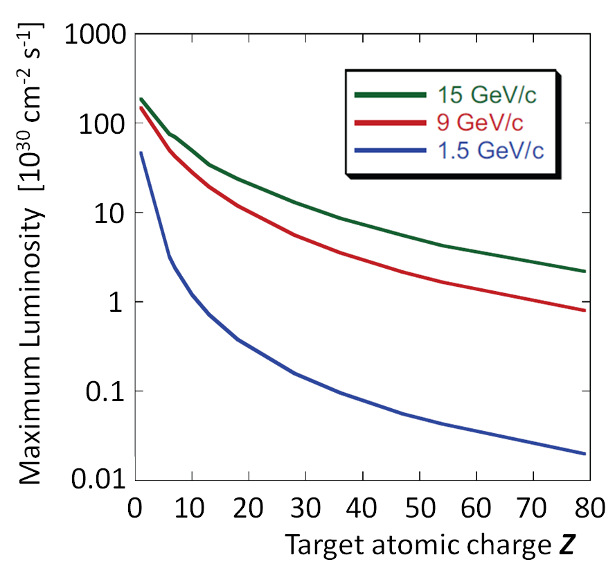
In case of nuclear targets the total hadronic cross section for the interaction of antiprotons with target nucleons can be estimated from geometric considerations taking into account the proton radius of fm and the radius of a spherical nucleus , which can be roughly approximated as , where fm and is the mass number. With the assumption that , the required total hadronic cross section, , for a nucleus of mass number can be extracted from the given values of for antiproton-proton collisions as follows:
| (1.3) |
Simulation results on maximum average luminosities based on equation 1.3 are shown in figure 1.7. They include adapted beam losses in the target due to single Coulomb scattering and energy straggling. Compared to antiproton-proton experiments, the maximum average luminosity for nuclear targets decreases rapidly with both, higher atomic charge and lower beam momenta, by up to three orders of magnitude. Specific values for selected nuclear targets are given in table 1.3 with the effective target thickness required to reach these numbers.
| Target | ||||||
|---|---|---|---|---|---|---|
| material | [\gevc] | [cm-2s-1] | [cm-2s-1] | [mbarn] | [s-1] | |
| hydrogen | 1.5 | () | 100 | 3.7 | ||
| 15 | () | 51 | 2.1 | |||
| argon | 1.5 | () | 2020 | – | ||
| 15 | () | 1030 | ||||
| gold | 1.5 | () | 7670 | – | ||
| 15 | () | 3911 |
Event Rates
Besides the cycle-averaged luminosity an evaluation of the instantaneous luminosity during the data taking is indispensable for performance studies of the \pandadetector. Associated event rates define the maximum data load to be handled at different timescales by the individual subsystems. The discussions in this section are based on the following assumptions:
-
•
Nominal antiproton production rate at \FAIR:
s-1 -
•
Effective target density:
atoms/cm2 -
•
Maximum number of antiprotons in the \HESR:
= 1011 -
•
Recycling of residual antiprotons at the end of each cycle
As indicated in figure 1.6 the instantaneous luminosity during the cycle changes on a macroscopic timescale. One elegant way to provide constant event rates in case of a cluster-jet target is given by the possibility to compensate the antiproton consumption during an accelerator cycle by the increase of the effective target density. Alternatively, using a constant target beam density the beam-target overlap might be increased adequately to the beam consumption. With these modifications the instantaneous luminosity during the cycle is expected to be kept constant to a level of 10%.
The values for the luminosity as given in table 1.2 are averaged over the full cycle time. However, to extract the luminosity during data taking, , these numbers must be rescaled to consider the time average over the experimental time:
| (1.4) |
In addition to the fluctuation of the instantaneous luminosity during the operation cycle as dicussed above (), it must be considered that the \HESRwill be only filled by 90% in case of using a barrier-bucket system. As a consequence, values for during data taking are 10% higher than the ones for .
An estimate of peak luminosities, , must further include possible effects on a short timescale. Contrary to homogeneous cluster beams, a distinct time structure is expected for the granular volume density distribution of a pellet beam. Such time structure depends on the transverse and longitudinal overlap between single pellets and the circulating antiproton beam in the interaction region. Deviations of the instantaneous luminosity on a microsecond timescale are caused by variations of the pellet size, the pellet trajectory and the interspacing between consecutive pellets. The latter must be well controlled to avoid the possible presence of more than one pellet in the beam at the same instant. The resulting ratio depends on the pellet size. First studies on the expected peak values for the \pandapellet target have been performed [Smirnov:2009]. Results indicate that the peak luminosity stays below cm-2s-1 if the pellet size is not bigger than 20 m.
Finally, for the extraction of event rates the obtained luminosities are multiplied with the hadronic cross section. Table 1.4 summarises the main results for a hydrogen target based on a pellet system, which is expected to deliver upper limits for the occuring event rates. In addition, a rough estimate for nuclear targets based on the input of table 1.3 and equation 1.3 is given. Even though these values still must be verified by detailed studies, it can be seen that the reduced average luminosity for heavier nuclear targets is counter-balanced by an increased cross-section that results in comparable event rates.
Based on the given assumptions and caveats, as discussed in this section, a nominal interaction rate of s-1 can be defined that all detector systems have to be able to handle. This specification includes the requirement that density fluctuations of the beam-target overlap have to be smaller than a factor of two (). However, in order to avoid data loss it might be important to introduce a generic safety factor that depends on special features of the individual detector subsystems and their position with respect to the interaction region.
1.2 The \PANDADetector
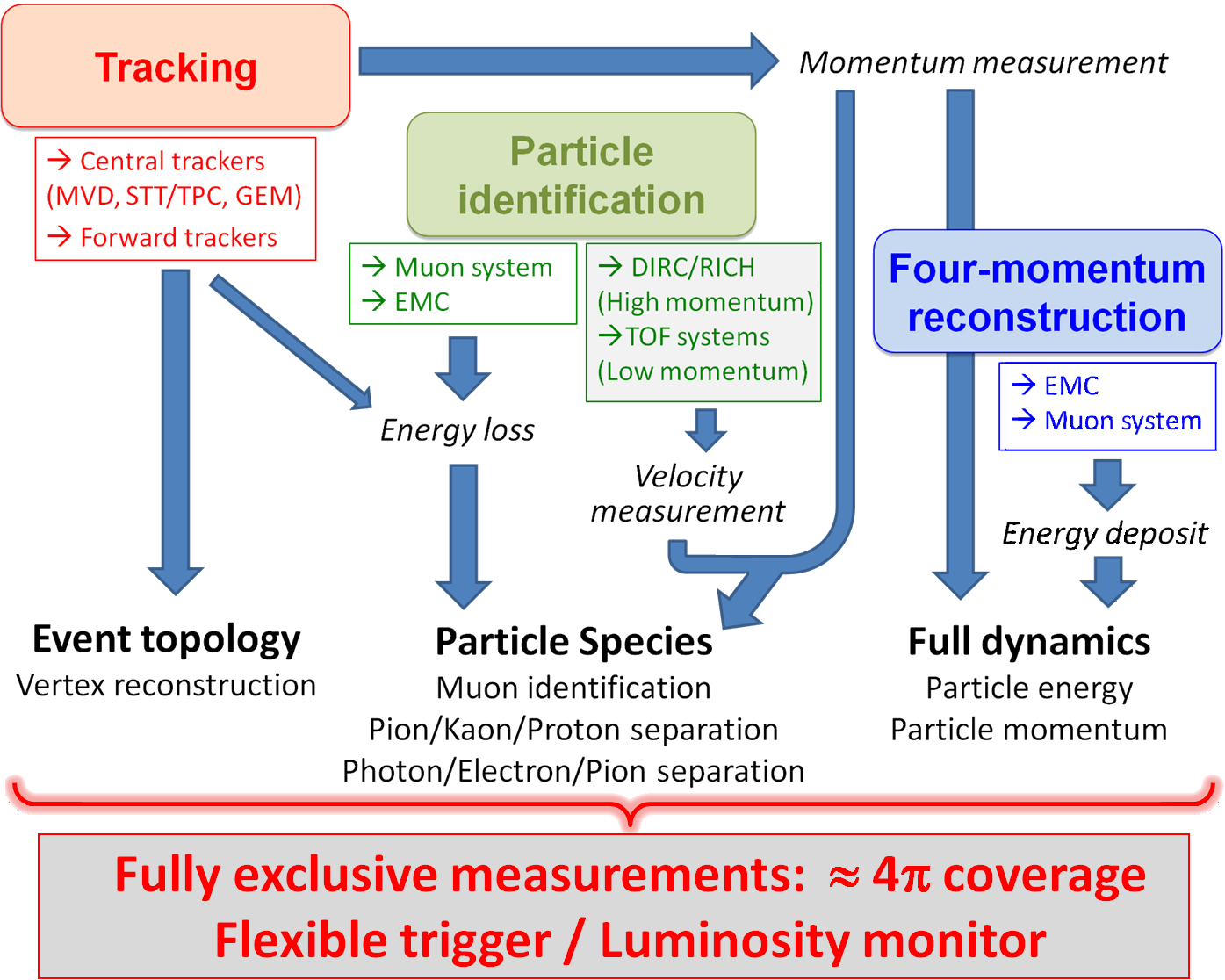
The main objectives of the design of the \PANDAexperiment are to achieve acceptance, high resolution for tracking, particle identification and calorimetry, high rate capabilities and a versatile readout and event selection. To obtain a good momentum resolution the detector will be composed of two magnetic spectrometers: the Target Spectrometer (TS), based on a superconducting solenoid magnet surrounding the interaction point, which will be used to measure at large polar angles and the Forward Spectrometer (FS), based on a dipole magnet, for small angle tracks. An overview of the detection concept is shown in figure 1.8.
It is based on a complex setup of modular subsystems including tracking detectors (MVD, STT, GEM), electromagnetic calorimeters (EMC), a muon system, Cherenkov detectors (DIRC and RICH) and a time-of-flight (TOF) system. A sophisticated concept for the data acquisition with a flexible trigger is planned in order to exploit at best the set of final states relevant for the \PANDAphysics objectives.
1.2.1 Target Spectrometer
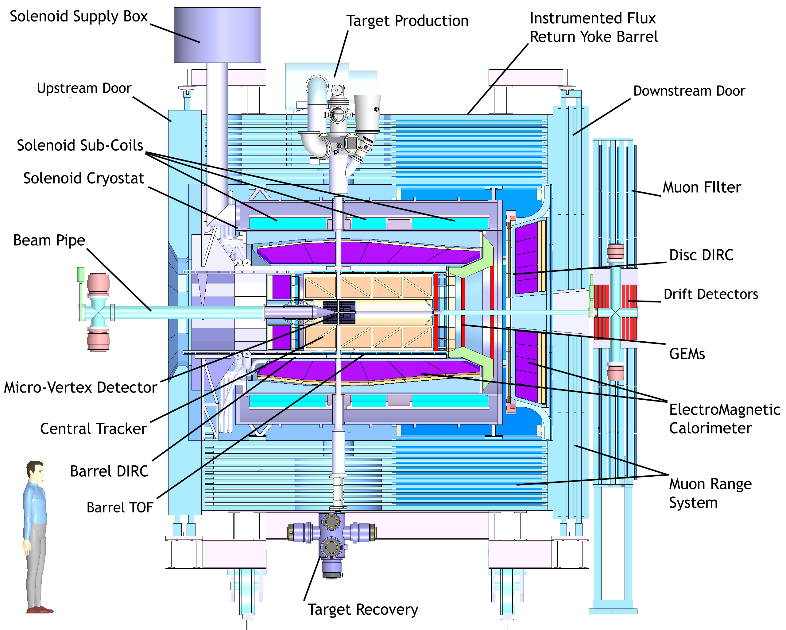
The Target Spectrometer will surround the interaction point and measure charged tracks in a highly homogeneous solenoidal field. In the manner of a collider detector it will contain detectors in an onion shell like configuration. Pipes for the injection of target material will have to cross the spectrometer perpendicular to the beam pipe.
The Target Spectrometer will be arranged in three parts: the barrel covering angles between 22 and 140, the forward end cap extending the angles down to 5 and 10 in the vertical and horizontal planes, respectively, and the backward end cap covering the region between about 145 and 170. Please refer to figure 1.9 for an overview.
Beam-Target System
The beam-target system consists of the apparatus for the target production and the corresponding vacuum system for the interaction region. The beam and target pipe cross sections inside the target spectrometer are decreased to an inner diameter of 20 mm close to the interaction region. The innermost parts are planned to be made of beryllium, titanium or a suited alloy which can be thinned to wall thicknesses of 200 m. Due to the limited space and the constraints on the material budget close to the IP, vacuum pumps along the beam pipe can only be placed outside the target spectrometer. Insections are foreseen in the iron yoke of the magnet which allow the integration of either a pellet or a cluster-jet target. The target material will be injected from the top. Dumping of the target residuals after beam crossing is mandatory to prevent backscattering into the interaction region. The entire vacuum system is kept variable and allows an operation of both target types. Moreover, an adaptation to non-gaseous nuclear wire targets is possible. For the targets of the planned hypernuclear experiment the whole upstream end cap and parts of the inner detector geometry will be modified. A detailed discussion of the different target options can be found in chapter 1.1.3.
Solenoid Magnet
The solenoid magnet of the TS will deliver a very homogeneous solenoid field of 2 T with fluctuations of less than 2%. In addition, a limit of mm is specified for the normalised integral of the radial field component. The superconducting coil of the magnet has a length of 2.8 m and an inner diameter of 90 cm, using a laminated iron yoke for the flux return. The cryostat for the solenoid coils is required to have two warm bores of 100 mm diameter, one above and one below the target position, to allow for insertion of internal targets. The load of the integrated inner subsystems can be picked up at defined fixation points. A precise description of the magnet system and detailed field strength calculations can be found in [PANDA-MagnetTDR].
Micro Vertex Detector
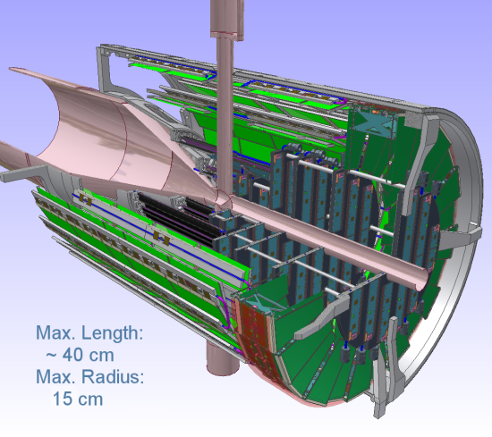
The design of the Micro Vertex Detector (\Mvd) for the Target Spectrometer is optimised for the detection of secondary decay vertices from charmed and strange hadrons and for a maximum acceptance close to the interaction point. It will also strongly improve the transverse momentum resolution. The setup is depicted in figure 1.10.
The concept of the \Mvdis based on radiation hard silicon pixel detectors with fast individual pixel readout circuits and silicon strip detectors. The layout foresees a four layer barrel detector with an inner radius of 2.5 cm and an outer radius of 13 cm. The two innermost layers will consist of pixel detectors and the outer two layers will be equipped with double-sided silicon strip detectors.
Six detector wheels arranged perpendicular to the beam will achieve the best acceptance for the forward part of the particle spectrum. While the inner four layers will be made entirely of pixel detectors, the following two will be a combination of strip detectors on the outer radius and pixel detectors closer to the beam pipe.
Additional Forward Disks
Two additional silicon disk layers are considered further downstream at around 40 cm and 60 cm to achieve a better acceptance of hyperon cascades. They are intended to be made entirely of silicon strip detectors. Even though they are not part of the central MVD it is planned, as a first approach, to follow the basic design as defined for the strip disks of the MVD. However, an explicit design optimisation still has to be performed. Two of the critical points to be checked are related to the increased material budget caused by these layers and the needed routing of cables and supplies for these additional disks inside the very restricted space left by the adjacent detector systems.
Straw Tube Tracker (\Stt)
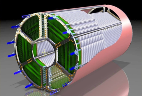
This detector will consist of aluminised Mylar tubes called straws. These will be stiffened by operating them at an overpressure of 1 bar which makes them self-supporting. The straws are to be arranged in planar layers which are mounted in a hexagonal shape around the \Mvdas shown in figure 1.11. In total there are 27 layers of which the 8 central ones are skewed, to achieve an acceptable resolution of 3 mm also in (parallel to the beam). The gap to the surrounding detectors will be filled with further individual straws. In total there will be 4636 straws around the beam pipe at radial distances between 15 cm and 41.8 cm with an overall length of 150 cm. All straws have a diameter of 10 mm and are made of a 27 m thick Mylar foil. Each straw tube is constructed with a single anode wire in the centre that is made of 20 m thick gold plated tungsten The gas mixture used will be Argon based with CO2 as quencher. It is foreseen to have a gas gain not greater than 105 in order to warrant long term operation. With these parameters, a resolution in and coordinates of less than 150 m is expected. A thin and light space frame will hold the straws in place, the force of the wire however is kept solely by the straw itself. This overall design results in a material budget of 1.2% of one radiation length.
Forward GEM Detectors
Particles emitted at angles below 22\degrees which are not covered fully by the STT will be tracked by three planar stations placed approximately 1.1 m, 1.4 m and 1.9 m downstream of the target. Each of the station consists of double planes with two projections per plane. The stations will be equipped with Gaseous micro-pattern detectors based on Gas Electron Multiplier (GEM) foils as amplification stages. The chambers have to sustain a high counting rate of particles peaked at the most forward angles due to the relativistic boost of the reaction products as well as due to the small angle \pbarpelastic scattering. The maximum expected particle flux in the first chamber in the vicinity of the 5 cm diameter beam pipe will be about cm-2s-1.
Barrel DIRC
At polar angles between 22\degrees and 140\degrees, particle identification will be performed by the Detection of Internally Reflected Cherenkov (\Dirc) light as realised in the \INSTBaBar detector [Staengle:1997xp]. It will consist of 1.7 cm thick fused silica (artificial quartz) slabs surrounding the beam line at a radial distance of 45 cm to 54 cm. At \INSTBaBar the light was imaged across a large stand-off volume filled with water onto 11,000 photomultiplier tubes. At \Panda, it is intended to focus the images by lenses onto Micro-Channel Plate PhotoMultiplier Tubes (MCP PMTs) which are insensitive to magnet fields. This fast light detector type allows a more compact design and the readout of two spatial coordinates.
Forward End-Cap DIRC
A similar concept is considered to be employed in the forward direction for particles at polar angles between 5\degrees and 22\degrees. The same radiator, fused silica, is to be employed, however in shape of a disk. The radiator disk will be 2 cm thick and will have a radius of 110 cm. It will be placed directly upstream of the forward end cap calorimeter. At the rim around the disk the Cherenkov light will be measured by focusing elements. In addition measuring the time of propagation the expected light pattern can be distinguished in a 3-dimensional parameter space. Dispersion correction is achieved by the use of alternating dichroic mirrors transmitting and reflecting different parts of the light spectrum. As photon detectors either silicon photomultipliers or microchannel plate PMTs are considered.
Scintillator Tile Barrel (Time-of-Flight)
For slow particles at large polar angles, particle identification will be provided by a time-of-flight (TOF) detector positioned just outside the Barrel DIRC, where it can be also used to detect photon conversions in the DIRC radiator. The detector is based on scintillator tiles of size, individually read out by two Silicon PhotoMultipliers per tile. The full system consists of 5,760 tiles in the barrel part and can be augmented also by approximately 1,000 tiles in forward direction just in front of the endcap disc DIRC. Material budget and the dimension of this system are optimised such that a value of less than 2% of one radiation length, including readout and mechanics and less than 2 cm radial thickness will be reached, respectively. The expected time resolution of 100 ps will allow precision timing of tracks for event building and fast software triggers. The detector also provides well timed input with a good spatial resolution for online pattern recognition.
Electromagnetic Calorimeters
Expected high count rates and a geometrically compact design of the Target Spectrometer require a fast scintillator material with a short radiation length and Molière radius for the construction of the electromagnetic calorimeter (\Emc). Lead tungsten (PbWO4) is a high density inorganic scintillator with sufficient energy and time resolution for photon, electron, and hadron detection even at intermediate energies [Mengel:1998si, Novotny:2000zg, Hoek:2002ss].
The crystals will be 20 cm long, i.e. approximately 22 , in order to achieve an energy resolution below 2\percent at 1 [Mengel:1998si, Novotny:2000zg, Hoek:2002ss] at a tolerable energy loss due to longitudinal leakage of the shower. Tapered crystals with a front size of will be mounted in the barrel EMC with an inner radius of 57 cm. This implies 11,360 crystals for the barrel part of the calorimeter. The forward end cap EMC will be a planar arrangement of 3,600 tapered crystals with roughly the same dimensions as in the barrel part, and the backward end cap EMC comprises of 592 crystals. The readout of the crystals will be accomplished by large area avalanche photo diodes in the barrel and in the backward end cap, vacuum photo-triodes will be used in the forward end cap. The light yield can be increased by a factor of about 4 compared to room temperature by cooling the crystals down to .
The EMC will allow to achieve an / ratio of 103 for momenta above 0.5 \gevc. Therefore, /-separation will not require an additional gas Cherenkov detector in favour of a very compact geometry of the EMC. A detailed description of the detector system can be found in [PANDA:TDR:EMC].
Muon Detectors
The laminated yoke of the solenoid magnet acts as a range system for the detection of muons. There are 13 sensitive layers, each 3 cm thick (layer “zero” is a double-layer). They alternate with 3 cm thick iron absorber layers (first and last iron layers are 6 cm thick), introducing enough material for the absorption of pions in the \PANDAmomentum range and angles. In the forward end cap more material is needed due to the higher momenta of the occurring particles. Therefore, six detection layers will be placed around five iron layers of 6 cm each within the downstream door of the return yoke, and a removable muon filter with additional five layers of 6 cm iron and corresponding detection layers will be moved in the space between the solenoid and the dipole.
As sensors between the absorber layers, rectangular aluminum Mini Drift Tubes (MDT) are foreseen. Basically, these are drift tubes with additional capacitive coupled strips, read out on both ends to obtain the longitudinal coordinate. All together, the laminated yoke of the solenoid magnet and the additional muon filters will be instrumented with 2,600 MDTs and 700 MDTs, respectively.
Hypernuclear Detector
The hypernuclei study will make use of the modular structure of \Panda. Removing the backward end cap calorimeter and the \Mvdwill allow to add a dedicated nuclear target station and the required additional detectors for spectroscopy close to the entrance of \Panda. While the detection of hyperons and low momentum can be ensured by the universal detector and its PID system, a specific target system and a -detector are additional components required for the hypernuclear studies.
The production of hypernuclei proceeds as a two-stage process. First hyperons, in particular \CascadeCascadebar, are produced on a nuclear target. In addition, a secondary target is needed for the formation of a double hypernucleus. The geometry of this secondary target is determined by the short mean life of the \Cascademinusof only 0.164 ns. This limits the required thickness of the active secondary target to about 25 mm to 30 mm. It will consist of a compact sandwich structure of silicon micro-strip detectors and absorbing material. In this way the weak decay cascade of the hypernucleus can be detected in the sandwich structure.
An existing germanium-array with refurbished readout will be used for the -spectroscopy of the nuclear decay cascades of hypernuclei. The main limitation will be the load due to neutral or charged particles traversing the germanium detectors. Therefore, readout schemes and tracking algorithms are presently being developed which will enable high resolution -spectroscopy in an environment of high particle flux.
1.2.2 Forward Spectrometer
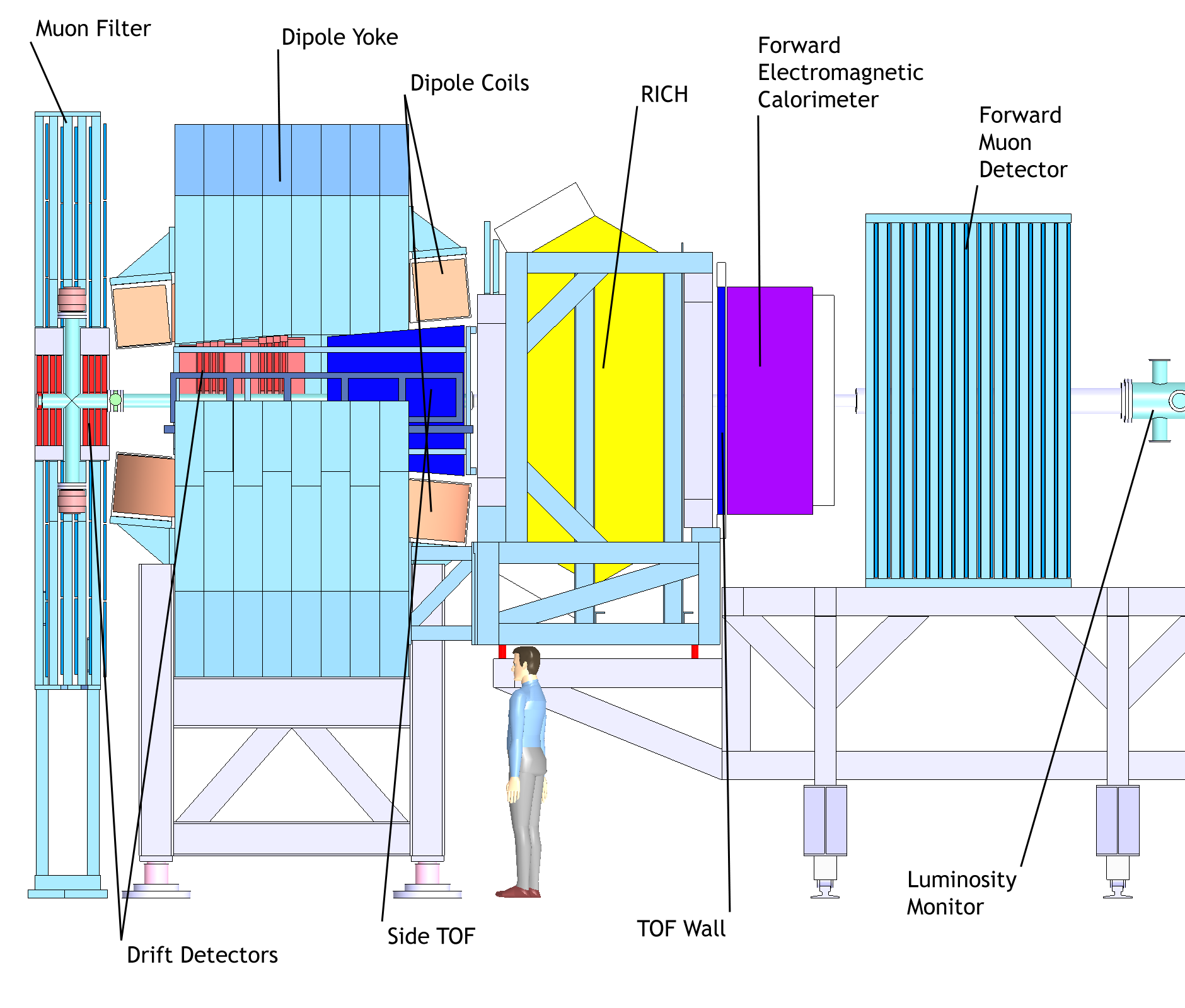
The Forward Spectrometer (FS) will cover all particles emitted in vertical and horizontal angles below and , respectively. Charged particles will be deflected by an integral dipole field. Cherenkov detectors, calorimeters and muon counters ensure the detection of all particle types. Figure 1.12 gives an overview to the instrumentation of the FS.
Dipole Magnet
A 2 Tm dipole magnet with a window frame, a 1 m gap, and more than 2 m aperture will be used for the momentum analysis of charged particles in the FS. In the current planning, the magnet yoke will occupy about 1.6 m in beam direction starting from 3.9 m downstream of the target. Thus, it covers the entire angular acceptance of the TS of 10\degrees and 5\degrees in the horizontal and in the vertical direction, respectively. The bending power of the dipole on the beam line causes a deflection of the antiproton beam at the maximum momentum of 15 of 2.2\degrees. For particles with lower momenta, detectors will be placed inside the yoke opening. The beam deflection will be compensated by two correcting dipole magnets, placed around the \Pandadetection system. The dipole field will be ramped during acceleration in the \HESRand the final ramp maximum scales with the selected beam momentum.
Forward Trackers
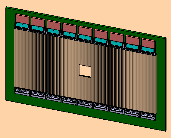
The deflection of particle trajectories in the field of the dipole magnet will be measured with three pairs of tracking drift detectors. The first pair will be placed in front, the second within and the third behind the dipole magnet. Each pair will contain two autonomous detectors, thus, in total, 6 independent detectors will be mounted. Each tracking detector will consist of four double-layers of straw tubes (see figure 1.13), two with vertical wires and two with wires inclined by a few degrees. The optimal angle of inclination with respect to vertical direction will be chosen on the basis of ongoing simulations. The planned configuration of double-layers of straws will allow to reconstruct tracks in each pair of tracking detectors separately, also in case of multi-track events.
Forward Particle Identification
To enable the / and / separation also at the highest momenta a \Richdetector is proposed. The favoured design is a dual radiator \Richdetector similar to the one used at \INSTHERMES [Akopov:2000qi]. Using two radiators, silica aerogel and C4F10 gas, provides // separation in a broad momentum range from 2 to 15 . The two different indices of refraction are 1.0304 and 1.00137, respectively. The total thickness of the detector is reduced to the freon gas radiator (5%), the aerogel radiator (2.8%), and the aluminum window (3%) by using a lightweight mirror focusing the Cherenkov light on an array of photo-tubes placed outside the active volume.
A wall of slabs made of plastic scintillator and read out on both ends by fast photo-tubes will serve as time-of-flight stop counter placed at about 7 m from the target. Similar detectors will be placed inside the dipole magnet opening to detect low momentum particles which do not exit the dipole magnet. The time resolution is expected to be in the order of 50 ps thus allowing a good / and / separation up to momenta of 2.8 \gevcand 4.7 \gevc, respectively.
Forward Electromagnetic Calorimeter
For the detection of photons and electrons a Shashlyk-type calorimeter with high resolution and efficiency will be employed. The detection is based on lead-scintillator sandwiches read out with wave-length shifting fibres passing through the block and coupled to photo-multipliers. The lateral size of one module is and a length of 680 mm (). A higher spatial resolution will be achieved by sub-dividing each module into 4 channels of 55 mm55 mm size coupled to 4 PMTs. To cover the forward acceptance, 351 such modules, arranged in 13 rows and 27 columns at a distance of 7.5 m from the target, are required. With similar modules, based on the same technique as proposed for \PANDA, an energy resolution of [bib:emc:KOP99] has been achieved.
Forward Muon Detectors
For the very forward part of the muon spectrum, a further range tracking system consisting of interleaved absorber layers and rectangular aluminium drift-tubes is being designed, similar to the muon system of the TS, but laid out for higher momenta. The system allows discrimination of pions from muons, detection of pion decays and, with moderate resolution, also the energy determination of neutrons and anti-neutrons. The forward muon system will be placed at about 9 m from the target.
Luminosity Monitor
The basic concept of the luminosity monitor is to reconstruct the angle of elastically scattered antiprotons in the polar angle range from 3 mrad to 8 mrad with respect to the beam axis corresponding to the Coulomb-nuclear interference region. The luminosity monitor will consist of a sequence of four planes of double-sided silicon strip detectors located in the space between the downstream side of the forward muon system and the \HESRdipole needed to redirect the antiproton beam out of the \PANDAchicane back into the direction of the \HESRstraight stretch (i.e. between m and m downstream of the target). The planes are positioned as close to the beam axis as possible and are separated by 10 cm along the beam direction. Each plane consists of four wafers arranged perpendicular surrounding to the beam axis placed at top, down, right and left. In this way, systematic errors can be strongly suppressed. The silicon wafers will be located inside a vacuum chamber to minimise scattering of the antiprotons before traversing the tracking planes. With the proposed detector setup an absolute precision of about 3% on the time integrated luminosity is considered feasible for this detector concept at \PANDA.
1.2.3 Data Acquisition
In \PANDA, a data acquisition concept is being developed to be as much as possible matched to the complexity of the experiment and the diversity of physics objectives and the rate capability of at least events/s. Therefore, every sub-detector system is a self-triggering entity. Signals are detected autonomously by the sub-systems and are preprocessed. Only the physically relevant information is extracted and transmitted. This requires hit-detection, noise-suppression and clusterisation at the readout level. The data related to a particle hit, with a substantially reduced rate in the preprocessing step, is marked by a precise time stamp and buffered for further processing. The trigger selection finally occurs in computing nodes which access the buffers via a high-bandwidth network fabric. The new concept provides a high degree of flexibility in the choice of trigger algorithms. It makes trigger conditions available which are outside the capabilities of the standard approach.
1.2.4 Infrastructure
The experimental hall for \PANDAwith a planned floor space of will be located in the straight section at the east side of the \HESR. Within the elongated concrete cave the \Pandadetector together with auxiliary equipment, beam steering, and focusing elements will be housed. Moreover, the experimental hall will provide additional space for delivery of components and assembly of the detector parts. To allow for access during \HESRoperation the beam line is shielded. The floor space for the \Pandaexperiment including dipoles and focusing elements is foreseen to have an area of and a height of 8.5 m with the beam line at a height of 3.5 m. The general floor level of the \HESRis planned to be 2 m higher to facilitate transport of heavy equipment into the \HESRtunnel. A crane spans the whole area with a hook at a height of about 10 m. The TS with electronics and supplies will be mounted on rails which makes it retractable to parking positions outside of the \HESRbeam line area. In the south corner of the hall, a counting house complex with five floors is foreseen. It will contain supplies e.g. for power, high voltage, cooling water and gases (1st floor), provide space for the readout electronics and data processing (2nd floor) as well as the online computing farm (3rd floor) and house the hall electricity supplies and ventilation (5th floor). The fourth floor with the control room, a meeting room and social rooms for the shift crew will be at level with the surrounding ground. The supply point will be at the north-east area of the building. All other cabling, which will be routed starting at the counting house, will join these supply lines at the end of the rails system of the Target Spectrometer at the eastern wall. The temperature of the building will be moderately controlled. More stringent requirements with respect to temperature and humidity for the detectors have to be maintained locally. To facilitate cooling and avoid condensation, the Target Spectrometer will be kept in a tent with dry air at a controlled temperature.
1.3 The Charged Particle Tracking System
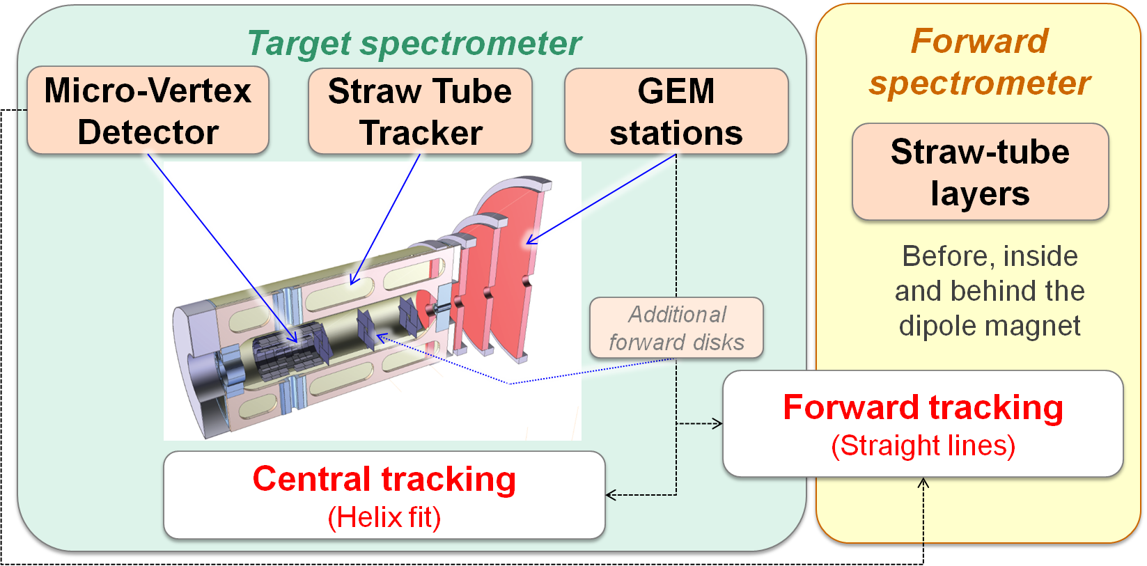
There are different tracking systems for charged particles at \PANDA, positioned inside the target spectrometer and in the forward region around the dipole magnet. Main tasks of the global tracking system are the accurate determination of the particle momenta, a high spatial resolution of the primary interaction vertex and the detection of displaced secondary vertices. Therefore, measurements of different subdetectors have to be merged in order to access the full tracking information.
1.3.1 Basic Approach
The magnetic solenoid field in the target spectrometer results in a circular transverse motion of charged particles with non-zero transverse momentum. The particle momentum then can be extracted via the determination of the bending radius. However, tracks with a small polar angle will exit the solenoid field too soon to be measured properly. For this case, the particle deflection induced by the subsequent dipole magnet is used to measure the particle momentum. Basically it can be deduced from a combined straight line fit before and after the dipole.
Due to the different analysing magnets, different track fitting algorithms have to be applied for central and forward tracks. Central tracks are reconstructed by combining hit points in the MVD layers with the hit information of the STT or the GEM stations. For the reconstruction of small angle tracks the straw tube layers in the forward spectrometer have to be used. In overlap regions the MVD, the additional forward disks or the GEM stations can contribute to the forward tracking because the delivery of an additional track point closer to the IP significantly improves the precision of the fitting results. After the global identification of individual tracks an event mapping have to be performed to match different tracks of the same event to a common vertex which either corresponds to the primary interaction vertex or a delayed decay of short-lived particles.
The luminosity monitor at the downstream end of the experiment is a tracking device of its own right. It was introduced to measure the time integrated luminosity, which is essential for the determination of cross sections for different physics processes. Therefore, elastically scattered antiprotons are measured under small angles corresponding to small momentum transfers. The associated differential cross sections are well known and thus provide an ideal reference channel. Additional information from the MVD will eventually improve the measurement by taking advantage of the reconstructed slow recoil proton at polar angles of around 90∘, which is correlated with the highly energetic antiproton detected in the luminosity monitor.
1.3.2 Optimisation Criteria
The different topics of the \PANDAphysics program will impose specific optimisation criteria and requirements to design and performance of the tracking system. The optimum design thus depends on the relative weight which is given to the different physics aspects. Main criteria for the optimisation will be discussed in the following.
Acceptance
Full azimuthal coverage is mandatory in order to allow identification of multi-particle final states and studies of correlations within the produced particles. In particular, the spectroscopy program of charmed and strange hadrons relies on the measurement of Dalitz plot distributions of three-body final states, which requires a smooth acceptance function across the full phase space. Particular care has to be taken to avoid gaps in the acceptance function and to minimise the effect of discontinuities induced by the transition between adjacent sub-detector components, by detector frames or by mechanical support structures.
The fixed-target setup at \PANDAimplies a Lorentz boost of the centre of mass ranging from 1.20 to 2.92. This large dynamic range in the Lorentz boost corresponds to a large difference in the typical event topologies at low and at high antiproton momenta. At higher antiproton beam momenta the vast majority of the produced particles in the final state will be emitted into the forward hemisphere. However, light particles like , or may well be emitted into the backward hemisphere even at highest beam momentum. As an example, pion backward emission is possible for a centre of mass momentum \mevcat \gevc, and for \mevcat \gevc.
Backward charged particle tracking is needed for various measurements foreseen at \PANDA. For instance, for the independent determination of the electric and magnetic parts of the time-like proton form factor in the reaction \pbarp \eethe full angular distribution has to be measured. At \gevcsq, that is at \gevc, a polar angle of in the centre of mass frame corresponds to electrons with a momentum of 0.70 \gevcat . Detection of pions in the backward hemisphere is important in studies of strange, multi-strange and charmed baryon resonances in \pbarp (+c.c.) reactions where the excited hyperon decays by single or double pion emission. Also higher charmonium states may emit pions with decay energies above the critical value for backward emission in the laboratory. The \PANDAtracking detectors therefore have to cover the full range of polar angles between and about .
Besides the solid angle of the detector also the acceptance in momentum space has to be considered. Often the final state contains charged particles with very large and with very small transverse momentum components which need to be reconstructed at the same time. Given the strength of the solenoid field of 2 T required to determine the momentum vector of the high transverse momentum particle, the radius of the transverse motion of the low transverse momentum particle may be small. Sufficient tracking capability already at small distance from the beam axis is therefore mandatory. As an example one may consider the reaction close to threshold with (& c.c.). Assuming 39 \mevcmomentum of the decay particles in the rest frame, particles of the subsequent decay (& c.c.) have 61 \mevcmomentum in the / rest frame. In the solenoid field of the TS, the charged pions and kaons from the / decay may have helix diameters up to almost 1.5 m. The transverse motion of the charged pion from the decay stays within a distance of almost 7 cm from the beam axis and therefore need to be reconstructed based on the track information from the MVD only.
Delayed Decay Vertex Detection
An important part of the \PANDAphysics program involves final states consisting of hadrons with open charm or strangeness which decay by weak interaction and thus have macroscopic decay lengths. The decay length of charmed hadrons is of the order of 100 m ( 310 m for , 150 m for , 120 m for , 130 m for , 60 m for , and 30 m for ). Therefore, the design of the tracking system aims on a detection of decay vertices of particles with decay lengths above 100 m. In order to achieve sufficient separation of the reconstructed decay vertex, the inner part of the tracking system has to be located very close to the interaction point, both in longitudinal and in radial direction. This requirement is fulfilled in the design of the MVD.
The identification of hyperons and mesons requires the reconstruction of delayed decay vertices at much larger distances. and hyperons have comparatively large decay lengths of about cm and cm, respectively. Due to the Lorentz boost this may result in vertices which are displaced by tens of centimetres from the interaction point mostly in the downstream direction. The considerations in the previous section concerning the required acceptance thus apply with respect to the shifted emission points of charged particles. The inner part of the \PANDAtracking system, therefore needs sufficient extension to the downstream direction in order to deliver sufficient track information for charged particle tracks originating from these displaced vertices.
Momentum and Spatial Resolution
The spatial resolution of the tracking detectors is important in two aspects. In the vicinity of the interaction point it directly determines the precision to which primary and displaced decay vertices can be reconstructed. Further on, based on the deflection of charged particles in both solenoid and dipole magnetic fields, it is an essential contribution to the momentum resolution of charged particles in all three coordinates.
The detection of displaced vertices of charmed hadrons imposes particular requirements to the spatial resolution close the interaction point. With a typical Lorentz boost , meson decay vertices have a displacement of the order of a few hundreds micrometres from the primary production point. Hence, to distinguish charged daughter particles of mesons from prompt particles a vertex resolution of 100 m is required. The position resolution is less demanding for the reconstruction of strange hadrons having decay lengths on the scale of centimeters. In this case a vertex resolution of a few millimetres is sufficient. Due to the significant Lorentz boost and the small opening angle between the decay particles of hyperons the resolution in transverse direction is required to be much better than the one for the longitudinal component.
The achievable momentum resolution is a complex function of the spatial resolution of the tracking sub-detectors, the number of track-points, the material budget of active and passive components resulting in multiple scattering, the strength and homogeneity of the magnetic field, and of the particle species, its momentum and its emission angle. Due to the respective momentum dependence, it is generally expected that multiple scattering limits the momentum resolution of low energy particles, whereas for high energy particles the smaller curvature of the tracks is the dominant contribution to the resolution.
The resolution in the determination of the momentum vectors of the final state particles directly determines the invariant or missing mass resolution of the particles that are to be reconstructed. Typically, the width of hadrons unstable with respect to strong interaction (except for certain narrow states like e.g. charmonium below the threshold) is of the order of 10 \mevccto 100 \mevcc. As an instrumental mass resolution much below the natural width is without effect, a value of a few 10 \mevccseems to be acceptable for the identification of known states or for the mass measurement of new states. With a typical scale of \gevccfor the kinematic particle energy this translates to a relative momentum resolution of the order of 1% as design parameter for the \PANDAtracking detectors.
Count Rate Capability
The expected count rates depend on the event rate as discussed in chapter 1.1.4 and the multiplicity of charged particles produced in the events. While the total rate is of importance for DAQ design and online event filtering, the relevant quantity for detector design and performance is the rate per channel, which is a function of the granularity per detector layer and of the angular distribution of the emitted particles. The latter depends on the beam momentum and the target material.
The nominal event rate at \PANDAis given by interactions per second. In case of annihilations typically only a few charged particles are produced. Even if secondary particles are taken into account, the number of charged particles per event will not be much larger than 10 in most cases. Thus the detector must able to cope with a rate of particles per second within the full solid angle. Particular attention has to be paid to elastic scattering since this process contributes significantly to the particle load in two regions of the detector: scattering of antiprotons at small forward angles and the corresponding emission of recoil protons at large angles close to . This affects primarily the inner region of the MVD disc layers and the forward tracking detector as well as the MVD barrel part and the central tracker.
The use of nuclear targets will not create significantly higher count rates than obtained with a hydrogen or deuterium target. This is due to single Coulomb scattering which dramatically increases with the nuclear charge () and results in losses with no related signals in the detector. In contrast to collisions in collisions no high rate of recoil particles close to is expected. The emission angles of recoil protons from quasi-free scattering are smeared by Fermi momentum and rescattering, while recoil nuclei, if they at all survive the momentum transfer, are too low energetic to pass through the beam pipe.
Particle Identification
Charged particle identification over a wide range of momentum and emission angle is an essential prerequisite for the capability of \PANDAto accomplish the envisaged physics program. Charged particles with higher momenta will be identified via Cherenkov radiation by the DIRC detector in the Target Spectrometer and by the forward RICH detector in the Forward Spectrometer. For positive charged kaon-pion separation in the DIRC about 800 \mevcmomentum is required. While almost all particles emitted within the acceptance of the Forward Spectrometer are above the Cherenkov threshold due to the forward Lorentz boost, a number of interesting reaction channels have final states with heavier charged particles () at larger angles with momenta below the DIRC threshold. In order to separate these low energy kaons from the much more abundant pions, particle identification capability based on energy loss information has to be supplied by the central tracking detector.
Material Budget
Any active or passive material inside the detector volume contributes to multiple scattering of charged particles, electron bremsstrahlung and photon conversion, and thus reduces the momentum resolution for charged particles in the tracking detectors, and detection efficiency and energy resolution for photons in the EMC. Therefore the material budget has to be kept as low as possible. Following the more demanding requirements to meet the performance criteria of the EMC, a total material budget of MVD and Central Tracker below 10% is still considered to be acceptable [PANDA:TDR:EMC].
References
Chapter 2 The Micro Vertex Detector – MVD
2.1 General Overview
This volume illustrates the technical layout and the expected performance of the Micro Vertex Detector (MVD) of the \PANDAexperiment. The introductory part contains a physics motivation that underlines the importance of this tracking system for key experiments at \PANDA. Basic detector requirements are defined taking into account both the demands of the scientific program and the experimental conditions of the antiproton accelerator \HESRas well as the \Pandatarget and detector setup. Moreover, the overall layout of the MVD is described.
Silicon detectors will be used as sensitive elements inside the MVD. The default option foresees hybrid pixel detectors and double-sided microstrip detectors in the inner and outer parts, respectively. Both of them are based on different detector technologies and thus impose specific requirements for the sensor production and characterisation, the connected \frontendelectronics and the hybridisation. Hence, all these topics will be discussed separately for the silicon pixel and the silicon strip part in chapter 3 and 4, respectively. Further aspects related to the MVD infrastructure, which are relevant for both parts, will be outlined in chapter 5. The performance of the MVD has been studied in extensive Monte Carlo simulations, which will be summarised in chapter 6.
2.2 Physics with the MVD
| particle | lifetime | decay length | decay channel (fraction) |
|---|---|---|---|
| 2.6842 | |||
| 311.8m | |||
| e.g. | |||
| 122.9m | |||
| e.g. | |||
| 149.9 m | |||
| e.g. | |||
| 7.89 | |||
| 2.404 | |||
| 4.434 | |||
| 4.91 | |||
| 2.461 | |||
| 59.9m | |||
| 33.6m |
| reaction channel | detected particle | tracking used for … |
| 2\Kp2\Km | momentum measurement (PID) | |
| \Kpm\pimp\Ks | momentum measurement (PID) | |
| \DDbar | \K’s and ’s | charm detection online |
| momentum measurement (PID) | ||
| \DDbar | \D(\Dbar) | inclusive charm ID online |
| \pip\pim ( / ) | vertex constraint |
Charged particle tracking is one of the essential parts in the overall detection concept at \PANDA, which aims at fully exclusive measurements with a flexible trigger. The MVD delivers 3D hit information close to the interaction point, which in addition defines the earliest possible measurement of particles in the reaction channel. Track and time information both provide important input for the subsequent event reconstruction. Precise timing is essential for an accurate assignment of individual tracks to the appropriate event. In addition, a fast detection of particles inside the MVD can be used as time reference for outer detector systems. The track information in the magnetic field of the solenoid gives access to the particle momentum and the event topology.
The identification of open charm and strangeness is one of the major tasks for the experiment. and hinges on the capability to resolve secondary decays of short-lived particles in displaced vertices other than the primary reaction point. In addition, the energy loss of slower protons, kaons and pions in the silicon detectors may be used as well to contribute to the global particle identification. Some examples of decay channels that hold the potential to be identified by purely geometrical means, are listed in table 2.1. Basically, strange and charmed hadrons exhibit two different decay length scales in the order of several centimetres and a few hundred micrometres, respectively. While \Pandawill focus on charm production, the identification of kaons will greatly enhance the efficiency also for mesons since they show large branchings into channels accompanied by kaons.
Key points of the \PANDAphysics program presented in chapter 1.1.1 can only be met with a suitable vertex resolution. In this context, the MVD will be of central importance for the associated physics goals. An identification of ground state mesons via their displaced vertex is of particular interest because they can be produced in associated decays of excited mesons as well as charmonia or charmonium-like states above the \DDbarthreshold. The applicability of a precise meson tagging is thus essential for the spectroscopy in the open charm sector and the charmonium mass region.
In addition, the experimental program at \Pandaputs emphasis on the high-resolution spectroscopy of electrons. Electrons are excellent tags for \Dmeson spectroscopy (cf. table 2.1). They carry information on the flavour of the decaying charm. With heavy targets leptons can also be used to reconstruct mesonic properties inside the nuclear medium.
Some of the envisaged physics benchmark channels, which all require the use of the vertex detector for quite different reasons, are listed in table 2.2. The most stringent requirements are given by those reaction channels where the \Ddecay will be used to select certain event patterns from the data stream during data acquisition, as indicated in the last column of the table.
2.3 Basic Detector Requirements
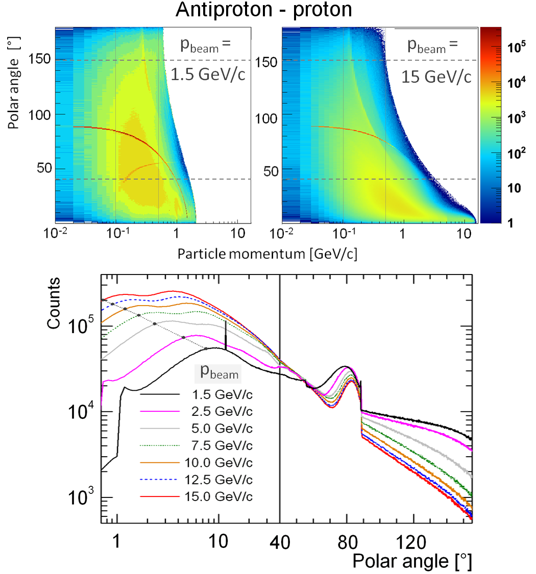
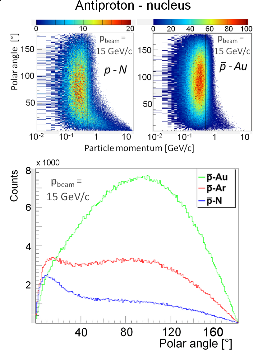
Basic detector requirements are mandated by the physics goals of the \Pandaexperiment and the experimental conditions the detector will meet during operation. The MVD has to cope with different experimental setups of the target region. In any case, before reaching the MVD particles must traverse at least one wall of the beam or target pipe. The minimum particle momentum for different particle species needed to reach the inner layer of the MVD is listed in table 2.3. Figure 2.1 illustrates the distribution of final state particles in antiproton-proton collisions at different beam momenta, which is expected to be obtained with a hydrogen target intended to be used in the first stage of \Panda.
| Particle | , | , |
|---|---|---|
| 89 MeV/c | 98 MeV/c | |
| 23 MeV/c | 25 MeV/c | |
| 56 MeV/c | 62 MeV/c | |
| 19 MeV/c | 21 MeV/c | |
| 1 MeV/c | 1 MeV/c |
The fixed-target setup is reflected by a Lorentz boost of particles in the forward direction, which increases with higher beam momentum. Most of these particles carry away a significant part of the initial beam momentum and thus the momentum range spans more than two orders of magnitude. Slower particles in a range of 100 \mevcup to 500 \mevcare emitted more or less isotropic over nearly the full solid angle. The elastic scattering process in antiproton-proton reactions delivers an enhanced emission of slow recoil protons at polar angles above 80∘. Results on the particle distribution in the final state to be expected with heavier targets are shown in figure 2.2. In comparison with antiproton-proton collisions the Lorentz boost in forward direction in antiproton-nucleus reactions is less distinct and vanishes with increasing atomic number.
Central task of the MVD is a precise measurement of both the primary interaction vertex and secondary decay vertices of short-lived particles. For this purpose the detection of a first track point very close to the nominal vertex is mandatory. Moreover, the obtained track information from the vertex detector also results in an improved momentum resolution. The general detection concept of \Pandarequests coverage over nearly the full solid angle. The boundary conditions of adjacent detector subsystems define a range of approximately 3∘ to 150∘ in polar angle to be covered by the MVD.
Due to the fixed-target setup, a very good spatial resolution is particularly needed in forward direction. Therefore, a high granularity and intrinsic detector resolution are a prerequisite. Slightly lower quality requirements result for the backward hemisphere. A sufficient number of track points must be measured inside the MVD to achieve an optimum tracking performance. In the best case, an independent pre-fit of MVD tracklets can be accomplished, for which a minimum of four track points is necessary. Further improvements can be achieved by an analogue readout of the signal amplitudes. It facilitates a cluster reconstruction over detector elements sharing the signal and additional energy loss measurements, which would be of advantage as they could be used in the particle identification at low energy.
Another main issue for the MVD is the minimisation of the material budget. \Pandawill have to cope with a large amount of low-energy particles. Scattering in the silicon layers is thus a major concern since the small-angle scattering drastically increases with decreasing particle energy. Moreover, any material near the primary target may cause background due to bremsstrahlung and pair production. The loss of photons related to the conversion or absorption in the detector material significantly affects the overall performance of the \Pandaapparatus,
As a consequence of the close position with respect to the interaction region all detector components must withstand an adequate radiation dose. With an overall lifetime of \Pandaof about 10 years and an assumed duty cycle of 50% the requested radiation tolerance given in terms of 1 \mevneutron equivalent particles per square centimetre, 1 \neueq, is in the order of \neueq [MVD-TIDstudy] and thus calls for dedicated production techniques. The achievable time resolution of the MVD must be in the order of 10 ns in order to cope with the high interaction rate. Particular challenges arise from the specific trigger and readout concept of the \Pandaexperiment that is based on an autonomous readout scheme for each of the individual detector sub-systems. Therefore, an internal trigger and a first data concentration must be integrated for each channel and on \frontendlevel, respectively. This approach exceeds common state-of-the-art solutions and required an extended research and development program.
In the following the most important detector requirements will be listed to conclude this section:
-
•
Optimum detector coverage
Within the given boundary conditions a full detector coverage must be envisaged. The number of layers is defined by the design goal, which foresees a minimum of four MVD hit points per track. An increased number of layers is necessary in the forward part in order to fulfill the required tracking performance. -
•
High spatial resolution
Tracks of charged hadrons have to be measured with a spatial resolution no worse than 100 m in and a few tens of m in . The achievable vertex resolution shall be in the same range of 100 m in order to resolve displaced decay vertices of open-charm states such as the and the with mean decay lengths of 123 m and 312 m, respectively (cf. table 2.1). One of the most demanding tasks is the recognition of \DDbarevents as decay products of charmonium states via their displaced vertices. At energies not much above the threshold, these mesons will be strongly forward focused. In this case, the best resolution is required along the beam (-direction). -
•
Low material budget
The impact of the MVD on the outer detector systems must be kept as low as possible. Photon conversion, in particular close to the interaction point, has to be minimised for the efficient operation of the electromagnetic calorimeter. Moreover, scattering deteriorates the overall tracking performance. In view of both deteriorating effects, the total material budget in units of radiation length, , shall stay below a value of . Besides the sole reduction of the total material amount, lightweight and low-Z materials must be used where ever possible. -
•
Improved momentum resolution
The track information of the MVD defines important constraints for the applied tracking algorithms and thus facilitates the determination of the particle momentum. In this context, it is of special importance for small-angle tracks. With the minimised material budget, matter effects will be reduced to such a level that the MVD can improve the overall momentum resolution by roughly a factor of two. -
•
Additional input to the global particle identification
The lower momenta for most of the emitted particles facilitate an improved particle identification based on energy loss measurements, which can provide additional to sustain different particles hypothesis. -
•
Fast and flexible readout
The readout has to be designed in a different way as compared to other experiments in order to allow continuous data collection from the detector without external triggering. As multiplicities are expected to be rather small (a maximum of 16 charged particles was estimated for the studies envisaged), the more serious aspect of data extraction from the vertex detector is caused by the rather high interaction rates, which will be in excess of 107 annihilations per second. The occupancy in different detector regions is very anisotropic and will also change due the use of different targets. This requires an efficient and flexible readout concept.
2.4 MVD Layout
The MVD is the innermost part of the central tracking system. Its position inside the \pandatarget spectrometer, the beam-target geometry and the resulting boundary conditions are shown in figure 2.3. In the following subsections, the basic geometry and the conceptual design of the detector will be discussed.
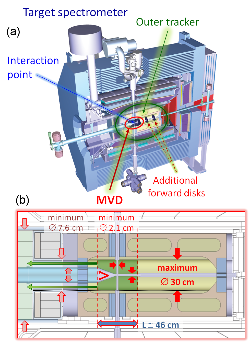
2.4.1 Basic Detector Geometry
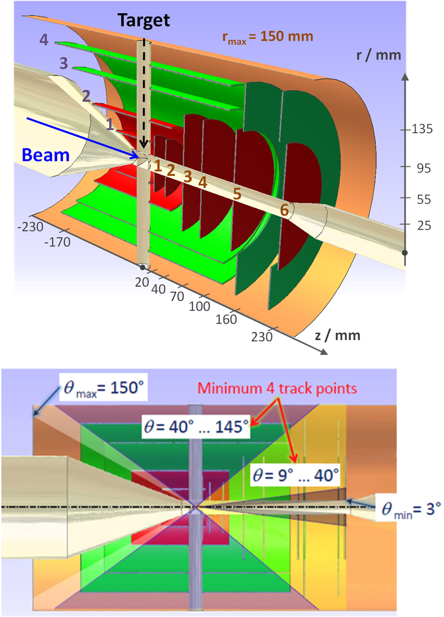
The MVD is divided into a barrel and a forward part. The outer limits are given by the detector position inside the central tracker, which defines a maximum radius of 15 cm. The extension of the MVD along the beam axis is roughly cm with respect to the nominal interaction point. A schematic picture of the MVD layers is shown in figure 2.4. There are four barrel layers and six forward disks. Silicon hybrid pixel detectors are foreseen in the two innermost barrel layers and for all disks. Double-sided silicon micro-strip detectors will be used in the two outer barrel layers and as radial complements in the last two disk layers. The basic detector layout results in a detector coverage with a minimum of four track points in a polar angle interval from 9∘ to 145∘.
The barrel part of the MVD covers polar angles between 40∘ and 150∘. The maximum downstream extension is given by both outer strip layers. The two pixel layers end at polar angles around 40∘ thus avoiding shallow crossing angles of particles. The upstream extension of all barrel layers is chosen to fit with the opening cone of the beam pipe. The radii of the innermost and the outermost barrel layer are set to 2.5 cm and 13.5 cm, respectively. The two intermediate barrel layers are arranged in increasing order.
The disk layers in forward direction enable a measurement at small polar angles between 3∘ and 40∘. The innermost disk located at cm is the closest of all detector layers with respect to the nominal interaction point. It has an interspacing of 2 cm to the second pixel disk. Both of these small pixel disks are located inside the outer pixel barrel layer. Further downstream there are four large pixel disks. While the first two of them are positioned inside the strip barrel layers, the ones still further downstream are outside the barrel layers and extended to larger radii by additional strip disks.
In addition to the MVD, there are two extra disks envisaged in forward direction that would fill the long detector-free gap to the forward GEM tracking station. They are intended to contribute to the vertex reconstruction of hyperons, which have much longer lifetimes and consequently a larger displacement of the secondary vertex than mesons. The conceptual design of these additional disks is similar to that of the strip disks of the MVD.
2.4.2 Conceptual Design
Choice of Detector Technology
Silicon detectors excel in a fast response and a low material budget. Moreover, they allow a high degree of miniaturisation and they can be produced in big quantities with very good reproducibility. Due to these properties they perfectly meet the requirements imposed on the MVD.
Silicon hybrid pixel detectors deliver discrete 2D information with a high granularity and allow very precise space point measurements. They are intended to be used in the innermost MVD layers in order to cope with the high occupancy close to the interaction region. However, the total number of channels required to cover larger surfaces increases rapidly.
The material budget of the detector scales with the number of readout channels. It must be minimised in order to fulfill the requirements of the \pandaexperiment. For this reason, double-sided silicon micro-strip detectors are foreseen in the outer parts of the MVD. They facilitate the readout of a much larger area with significantly fewer channels. However, an utilisation very close to the primary vertex is disfavored because of the high probability of multiple hits in the detector, which lead to ambiguities, so-called ghost hits, and the increased probability for hit loss due to pile-up.
In the following, all individual silicon detectors will be denoted as either pixel or strip sensors in order to avoid misinterpretations.
Hierarchical Structure
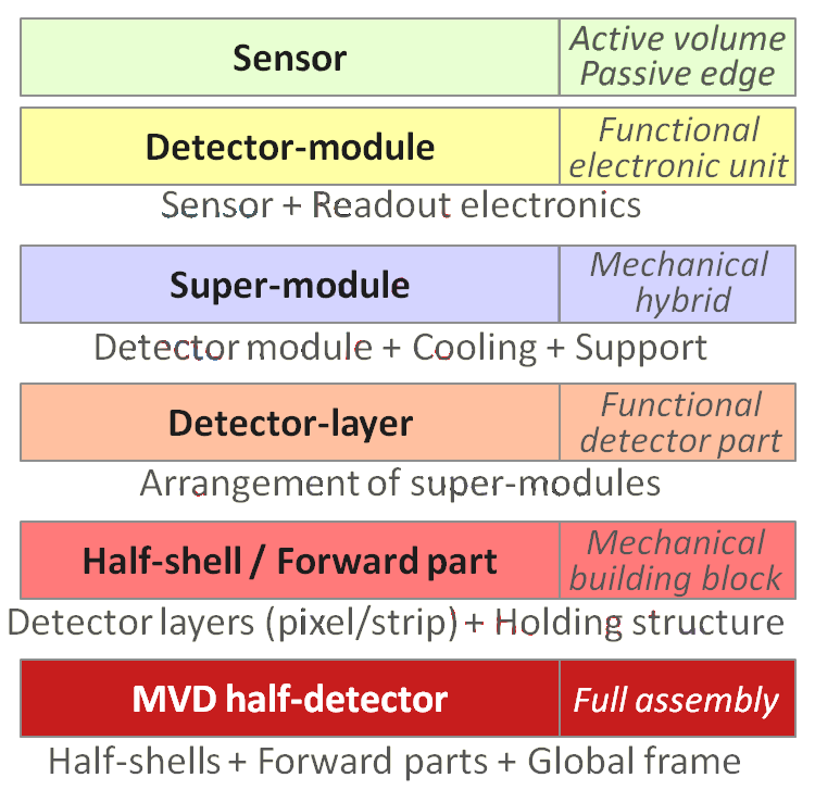
The hierarchical structure of the MVD is based on a modular concept following the future test and installation sequence of the detector. The silicon sensors represent the lowest level therein. A detector module is defined as the smallest functional unit, which is electronically independent. It is formed by all hard-wired connections between individual sensors and assigned components of the readout electronics.
The finalised hybrid is formed by a super-module including several detector modules and the associated cooling and support structure. It corresponds to the smallest mechanically independent unit for the detector assembly. Different detector layers are then composed of super-modules, which are attached to the respective mechanical holding structure. In this way four main building blocks are created. They are given by the individual pixel and strip layers, which form two half-shells in the barrel part and two half-disk structures in the forward part, respectively. The half-detector concept is required due to the target pipe, which crosses the entire MVD volume from the top to the bottom and thus breaks rotational symmetry around the beam axis. As a consequence, the detector will be left-right separated along its middle plane. A schematic picture of the hierarchy is given in figure 2.5.
Sensor Geometry
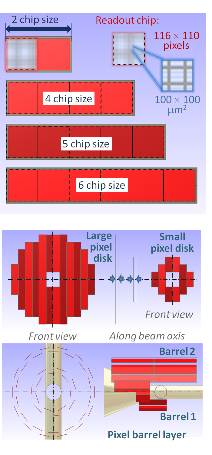
The schematic detector layers as shown in figure 2.4 must be approximated by an appropriate arrangement of individual detector elements. The precise sensor dimensions and the exact sensor positioning result from an explicit design optimisation [PhD-Tesis_Wuerschig]. It has been accomplished to facilitate compromise between good spatial coverage and minimum material on the one hand and the introduction of sufficient space needed for passive elements and appropriate safety margins for the detector integration on the other. Therefore, technical aspects have been taken into account alongside with purely geometric considerations. The final number of different sensor types is kept small in order to facilitate the modular concept and to obtain a high compatibility. The specific size of the readout structure has direct impact on the sensor design. For the two different detector types it is given by the pixel cell size and the strip interspacing, respectively.
In case of pixel sensors a rectangular shape is favored due to technical reasons. The \Pandapixel design is based on a quadratic pixel cell size with a side length of 100 m. There are four different pixel sensors, each of them has the same width but they differ in lengths. The dimensions correspond to multiples of the readout matrix of the connected readout chip, which serves cells (see chapter 3.3) and thus features an area of approximately 1.3 cm2. The different pixel sensor types are shown schematically in figure 2.6, on the top.
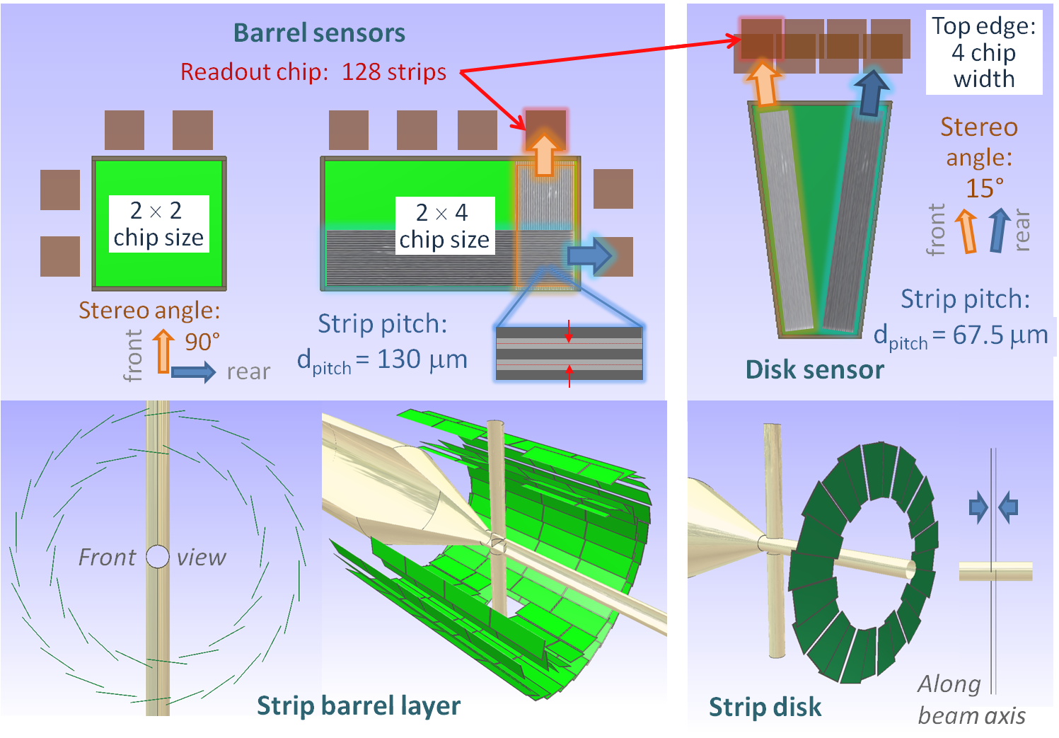
The basic geometry for the pixel sensor arrangement is illustrated below. A pixel barrel layer is made of a double-ring arrangement in order to achieve sufficient radial overlap. Shorter sensors are used to obtain sufficient space for the target pipe lead-through. The forward disk layers consist of an appropriate configuration of pixel sensors, which are aligned in different rows. Alternating rows are positioned with a small interspacing along the beam axis thus allowing the compensation of the passive edge around the active area.
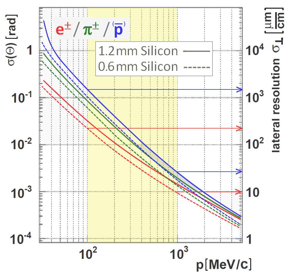
For silicon strip detectors there is no direct impact of the readout chip size on the dimension of the sensor segmentation. Hence, the distance between neighbouring strips, which is commonly denoted as “strip pitch”, is one of the main parameters for the detector optimisation. An approximate range is given by the average track deviation related to scattering effects in the previous pixel layers. Calculated values for the mean scattering angle and the associated deflection of tracks are shown in figure 2.8. They are obtained with an empirical formula for the multiple scattering in a Gaussian approximation given by Lynch and Dahl [ScatteringDahl].
| Basic parameter | Pixel part | Strip part |
|---|---|---|
| Number of super-modules | 66 | 70 |
| Number of detector modules | 176 | 140 |
| Number of sensors | 34 (2 chips size) | 172 (rectangular) |
| 28 (4 chips size) | 34 (squared) | |
| 54 (5 chips size) | 48 (trapezoidal) | |
| 60 (6 chips size) | ||
| Total: | 176 | 254 |
| Active silicon area / [m2] | 0.106 | 0.494 |
| Number of \frontendchips | 338 (barrels) | 940 (barrels) |
| 472 (disks) | 384 (disks) | |
| Total: | 810 | 1324 |
| Number of readout channels |
| Main | Sub-layer | () | () | ||||||
| layer | [mm] | [mm] | [mm] | [mm] | [mm] | [mm] | [mm] | [mm] | |
| Barrel | Inner ring | 25 | 22 | 21.80 | 22.75 | - | - | 39.8 | 9.8 |
| layer 1 | Outer ring | 28 | 27.80 | 28.58 | |||||
| Barrel | Inner ring | 50 | 47.5 | 47.30 | 47.85 | - | - | 79.8 | 57.8 |
| layer 2 | Outer ring | 52.5 | 52.30 | 52.82 | |||||
| Barrel | 95 | 92 | 89.72 | 96.86 | - | - | 133.8 | 139.0 | |
| layer 3 | |||||||||
| Barrel | 135 | 125 | 123.20 | 129.24 | - | - | 169.2 | 139.0 | |
| layer 4 | |||||||||
| Disk | Sdk 1, front | 50 | - | 11.70 | 36.56 | 20 | 22 | 19.7 | 19.9 |
| layer 1 | Sdk 1, rear | 24.1 | 24.3 | ||||||
| Disk | Sdk 1, front | 50 | - | 11.70 | 36.56 | 40 | 42 | 39.7 | 39.9 |
| layer 2 | Sdk 2, rear | 44.1 | 44.3 | ||||||
| Disk | Ldk 1, front | 95 | - | 11.70 | 73.96 | 70 | 72 | 69.7 | 69.9 |
| layer 3 | Ldk 1, rear | 74.1 | 74.3 | ||||||
| Disk | Ldk 2, front | 95 | - | 11.70 | 73.96 | 100 | 102 | 99.7 | 99.9 |
| layer 4 | Ldk 2, rear | 104.1 | 104.3 | ||||||
| Disk | Ldk 3, front | - | - | 11.70 | 73.96 | 160 | 150 | 147.7 | 147.9 |
| layer 5 | Ldk 3, rear | 152.1 | 152.3 | ||||||
| StripDk 1, L | - | - | 74.33 | 131.15 | 162.5 | 160.0 | 160.3 | ||
| StripDk 1, S | 165.0 | 165.3 | |||||||
| Disk | Ldk 4, front | - | - | 11.70 | 73.96 | 230 | 220 | 217.7 | 217.9 |
| layer 6 | Ldk 4, rear | 222.1 | 222.3 | ||||||
| StripDk 2, S | - | - | 74.33 | 131.15 | 207.5 | 204.7 | 205.0 | ||
| StripDk 2, L | 209.7 | 210.0 | |||||||
| Sdk … small pixel disk, Ldk … large pixel disk, StripDk … strip disk | |||||||||
Plotted results for a silicon thickness of 0.6 mm and 1.2 mm represent the minimum effective path lengths of particles crossing two and four pixel layers, respectively. With a minimum flight path of roughly 10 cm between the pixel and the barrel layers, the lateral track resolution due to scattering effects is restricted to a few hundred micrometers for particles with a momentum well below 1 \gevc.
In total there are three different strip sensor types, which have different shapes. They are shown in figure 2.7, on the top. Quadratic and rectangular sensors are chosen for the barrel part, while a trapezoidal design is used for the forward disks. The respective stereo angle is set to 90∘ in case of barrel type sensors and to a reduced angle of 15∘ for the trapezoids. In this way strips always run in parallel to one sensor edge. The strip pitch for the rectangular barrel sensors is set to 130 m. A smaller value of 67.5 m for the trapezoids in the disk part is used to recover the worsened resolution induced by the smaller stereo angle.
The strip barrel layers are formed by a paddle-wheel sensor arrangement. Neighbouring trapezoidal sensors of the forward disks are located at two positions slightly shifted along the beam axis in order to make up for the passive sensor edge. To accommodate the target pipe crossing, some barrel strip sensors are left out at the top and bottom. A schematic picture of the strip sensor geometry is given in the bottom part of figure 2.7.
Finally, the defined sensor geometry results in approximately 10.3 million pixel and roughly 200,000 strip readout channels. Design parameters for the MVD are summarised in table 2.5. A compilation of the sensor positions in all detector layers can be found in table 2.5.
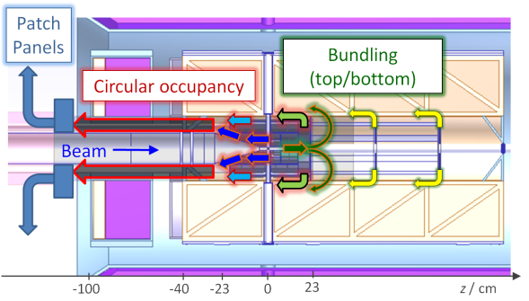
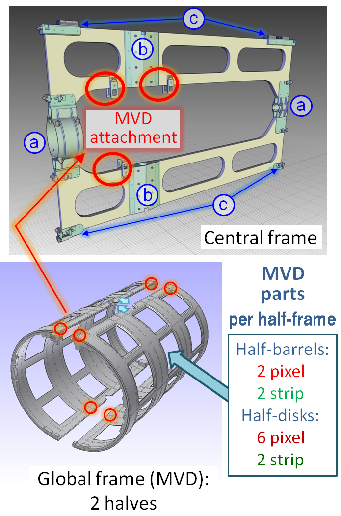
Mechanics and Detector Integration
The MVD will operate under normal pressure conditions at room temperature of approximately +25 ∘C. An active cooling of both pixel and strip readout electronics is needed for a long term stability of the detector. A detailed description of the cooling system can be found in chapter 5.6. Besides the cooling pipes, other service structures must be brought from the outside close to the silicon detectors in order to supply sensors and associated electronics components as well as to transmit signals for data and slow control of the readout chips. A schematic routing scheme for all MVD services is given in figure 2.9.
Limitations are given by the stringent boundary conditions. Due to the fixed target setup, which defines the physically most interesting region in the forward part, a guiding to the outside of the target spectrometer is only possible in upstream direction. In this region the opening cone of the beam pipe reduces the available cross section at inner radii. The restricted radial space requires a circular occupancy of all services around the beam pipe. For the pixel disk inside the barrel layers a bundling at the top and bottom is foreseen. Patch panels, which allow a connection to peripheral systems, are intended to be placed further upstream.
Basic ideas of the overall detector integration for the MVD are shown in figure 2.10. The mechanical interface to external parts of the \pandaapparatus is defined by a three point fixation to the central frame, which serves as reference frame and global support for the entire central tracking system. It also facilitates a consecutive assembly of the beam-target system, the MVD and the outer tracker outside of the solenoid magnet. A safe insertion of all attached sub-systems to their nominal position is realised via a rail system. The global support structure for the MVD is composed of two half-frames. Both halves are mechanically independent in order to avoid any introduction of stress to either half-detector. They allow the internal mounting of all detector half-layers and the attachment to the central frame. All support structures inside the MVD will be composed of light-weight carbon materials. Details can be found in section 5.5. Additional support structures are also needed for MVD services.
References
Chapter 3 Silicon Pixel Part
This chapter describes the silicon pixel part of the Micro Vertex Detector. The innermost layers and disks of the MVD are the most important ones for determining primary and secondary vertices of charm mesons. They need a very high precision and granularity to cope with the required spatial resolution. In addition they have to handle high track densities in the forward region for proton targets, they are exposed to relatively high radiation levels and they have to process and transmit very high data rates due to the untriggered readout of \PANDA. To cope with these requirements a hybrid pixel detector with its two-dimensional segmentation featuring a 2D readout without ambiguity, double hit resolution, excellent signal to noise ratio at high speed, and reliable sensor technology appears to be the most interesting choice for equipping the innermost part of the MVD.
3.1 Hybrid Pixel Assembly Concept
Hybrid pixel detectors have been studied and developed for the vertex trackers of the LHC experiment. The core issue is a two-dimensional matrix, the sensor (rectangular shape of few tens of mm by a few hundreds m thick), of reverse biased silicon diodes flip-chip bonded to several readout chips. Each cell (pixel) on the sensor matrix is connected by solder-lead bumps (alternatively indium is used) to a frontal cell on a readout ASIC developed in CMOS technology. The readout cell must fit into the same area as the pixel sensing element. In particular, the ASICs used in the LHC experiments have been developed in 250 nm CMOS technology, whereas the sensor has been made of Floating Zone (FZ) silicon with a minimum thickness of 200 m. The request of high granularity and the simulation results of benchmark channels for the MVD indicate a pixel size of as the most suitable. However the reduction of the surface of the pixel increases the perimeter-to-area ratio and hence the input capacitance, which is usually dominated by the inter-cell capacitance. To cope with the limited material budget an RD effort to investigate a lower sensor thickness has been made and the results are reported in chapter 3.2. Concerning the sensor material, references [semi0], [semi1] indicate that silicon epitaxial material could be an interesting material to be applied in \PANDA, in particular for radiation hardness, up to the radiation level expected. Taking into account the configuration of the wafer made of an epitaxial silicon layer grown on top of a Czochralski substrate, thinned pixel sensors could be obtained by removing most of the Cz substrate. Furthermore, an RD project has started to develop a readout ASIC in 130 nm CMOS technology equipped with pixel cells of the required size. In addition to the two-dimensional spatial information, time and energy loss of the hit will be measured. Besides the feature to obtain by this technology the same electrical functionality using a quarter of area than older technology with a power reduced by a factor 4 appears a challenge towards a simplification of the cooling system. The readout architecture is described in the section 3.3.3 and the ASIC prototypes in the section 3.3.5. A schematic view of the custom hybrid pixel assembly for the \PANDAexperiment is shown in figure 3.1.
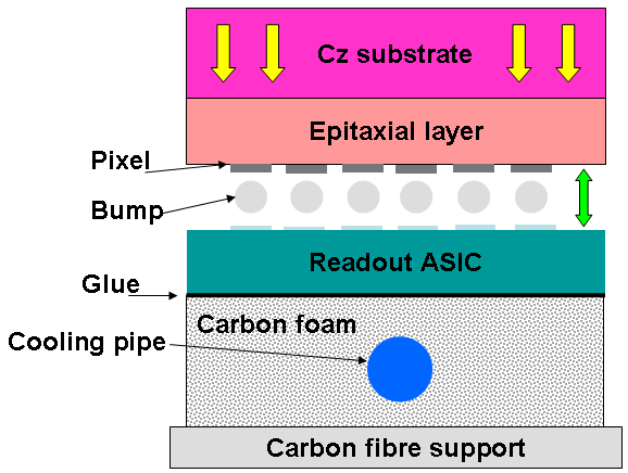
The epitaxial silicon layer with a thickness up to 150 m and a high resistivity of few kOhm cm is the active region of the pixel matrix. The Cz substrate features lower resistivity ( ) and a thickness of a few hundreds of m. Most of this substrate is removed starting from the side opposite to the epitaxial layer. Each pixel is connected by the bump bonding technique to the corresponding readout cell of a custom ASIC that will be developed in 130 nm CMOS technology. Then this assembly is glued to a carbon foam layer to improve heat dissipation towards the cooling pipe as a part of a cooling system working in depression mode and based on water as cooling fluid. A structure made of carbon fibre with suitable shape is the mechanical support.
3.2 Sensor
3.2.1 First Thinned Prototypes
To study the epitaxial silicon material, first prototypes of hybrid pixel assemblies using thinned epitaxial silicon pixel structures as sensor element have been produced and tested in 2008 [epi02]. Results were obtained from assemblies with three different epitaxial thicknesses of 50, 75 and 100 m. The \frontendchip for \PANDAwas still under development at that time and therefore ALICE pixel \frontendchips and readout chain were used. Basic detector characteristics, bump bond yields were measured, and tests with various radioactive sources were performed.
Design and Production
For the sensors, 4-inch wafers with three different n-epitaxial layer thicknesses deposited on standard Czochralski (Cz) substrate wafers were provided by ITME (Warsaw). The different epitaxial layer characteristics are shown in table 3.1. The Cz substrate parameters were equal for all wafers: conductivity type, Sb dopant, 525 m thickness, resistivity.
| Epi Layer | Thickness | Resistivity |
|---|---|---|
| Epi-50 | m | 4060 |
| Epi-75 | m | 4570 |
| Epi-100 | m | 4900 |
The wafers were processed by FBK-ITC (Trento) using ALICE pixel sensor masks provided by INFN-Ferrara which had already previously been used to produce high quality ALICE pixel assemblies from 200 m Float Zone (FZ) material [alice0]. The sensor masks include full-size and single-chip sensors (the ALICE pixel size is ) together with the usual range of diagnostic structures including simple diodes. Six epitaxial wafers were processed, two of each thickness. The thinning of the sensor wafers and the bump-bonding to ALICE pixel readout chips were performed by VTT (Finland). The target thicknesses for the sensor wafers were chosen to be 100, 120, and 150 m, respectively, for the 50, 75, and 100 m epi layers. Single chip sensors were bump-bonded to chip-sensor assemblies (Epi-50, Epi-75, and Epi-100, respectively, corresponding to the 50, 75, and 100 m thick epitaxial layers).
Results
The full-depletion voltage values for all three epitaxial wafer thicknesses were less than 6 V. Figure 3.2 shows the total sensor leakage current as a function of bias voltage up to 200 V for two assemblies.
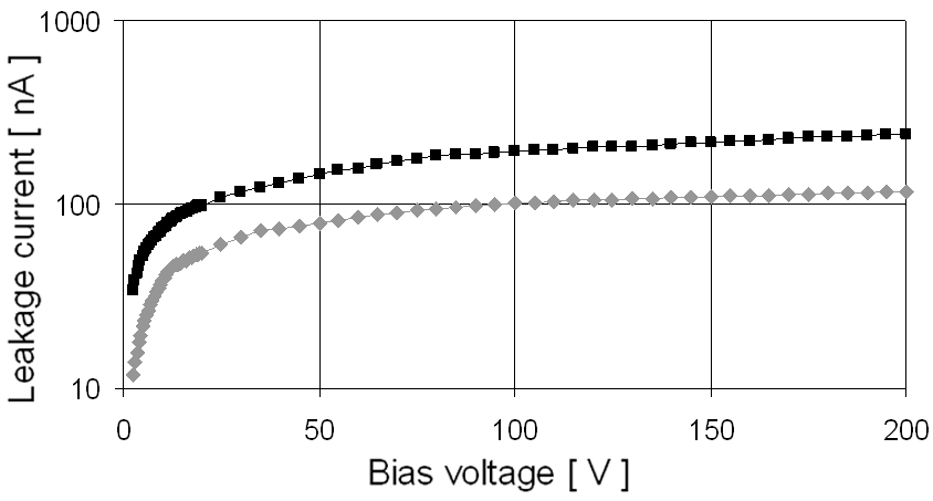
No sign of breakdown is observed, and the thicker sensor has a higher current for any given voltage. Good long-term stability was also noted. Total leakage current as a function of the bias voltage was measured at different temperatures up to 50 ∘C for one assembly (Epi-50). A leakage current of about 3 nA, corresponding to a bias voltage of 100 V, (the assembly has 8192 pixels) at 21 ∘C increases up to about 23 nA at 43 ∘C. This corresponds to a leakage current per pixel of less than about 10 fA, which is a value that can be accepted and controlled by the readout circuit.
Three assemblies, S15 (Epi-50), S8 (Epi-75), and S6 (Epi-100), were instead mounted on testing boards enabling their complete electrical characterisation using the ALICE Pixel DAQ system [alice1]. Beta particles from a 90Sr source, which pass through the assemblies and their associated mountings to subsequently trigger a plastic scintillator with photomultiplier readout should be sufficiently similar in their behaviour to minimum-ionising particles (MIP) to enable a relative comparison of the active thickness of the epitaxial sensors. Calibration of the threshold DAC setting in electrons is obtained by making similar, but selftriggered, threshold scans while exposing the assemblies to 55Fe and 109Cd Xray sources. Figure 3.3 shows the threshold value in electrons corresponding to the most probable value of the Landau distribution plotted with respect to the nominal epitaxial active thickness.
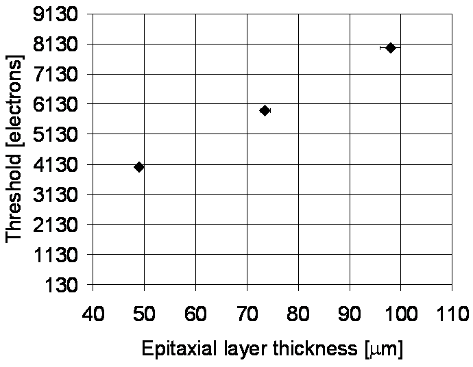
It should be noted, as is confirmed by the linearity of the result, that charge sharing is not a major issue despite the 50 m pixel width due to the fact that the active thickness is equally limited. Taking 22.500 electrons for a true MIP in 300 m of silicon one would expect 7500 electrons from 100 m of silicon, and given the use of the beta source which should raise that value somewhat the agreement seems more than satisfactory.
3.2.2 Radiation Damage Study
Epitaxial material has been studied for radiation damage by many experimental groups (RD50 collaboration). In particular, at the beginning of the RD phase for the \PANDApixel detector, results on thin epitaxial diodeds (about 25 m) and lower epitaxial resistivity (about ) were available. However the application of epitaxial material in the \PANDAexperiment asked for higher thickness and higher resistivity to obtain more electron production from MIP and a lower full depletion voltage, respectively. For these reasons systematic tests for radiation damage were planned. The most important parameters as full depletion voltage and leakage current have been studied as a function of fluences and annealing phases. To study the behaviour of these parameters, displacement damage tests were performed using neutrons from the nuclear reactor (TRIGA MARK II) of Pavia (Italy) at the LENA laboratory. Diodes from wafers, featuring different epitaxial thicknesses and resisitivity as reported in Table 3.2, have been characterised for full depletion voltage and leakage current using a probe station with bias voltage provided by a Keithley 237 High Voltage Source Measure Unit.
| Diodes | Thickness | Resistivity |
|---|---|---|
| Epi-50, HR | m | 4060 |
| Epi-75, HR | m | 4570 |
| Epi-100, HR | m | 4900 |
| Epi-50, MR | m | 3100 |
| Epi-75, MR | m | 3200 |
| Epi-100, MR | m | 3610 |
| Epi-75, LR | m | 460 |
I-V measurements have been performed using an HP4145B Semiconductor Parameter Analyser and C-V mesurements have been performed using an HP4248A Precision Meter. The measurents of I-V and C-V trends for different diodes have been carried out before and after the irradiation as a function of the equivalent fluence and specifically with the following values: and \neueq, respectively, corresponding to about 10 years of \PANDAlifetime with antiproton proton annihilation and antiproton Xe interactions (50% duty cycle).
Then, a long annealing phase at 60 ∘C was started and full depletion bias voltage and leakage current characterisation were performed many times during this period. The full depletion voltage is evaluated from the intersection of the two extrapolated lines in the capacitance-voltage characteristic. In Table 3.3 the full depletion voltage of diodes under test are reported before the irradiation.
| Diodes | Full Dep. Voltage [V] | [V] |
|---|---|---|
| Epi-50, HR | 4.35 | 0.06 |
| Epi-75, HR | 5.6 | 0.1 |
| Epi-100, HR | 5.9 | 0.2 |
| Epi-50, MR | 4.91 | 0.07 |
| Epi-75, MR | 8.2 | 0.3 |
| Epi-100, MR | 10.4 | 0.6 |
| Epi-75, LR | 42.6 | 1.3 |
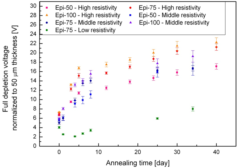
As expected the full depletion voltage values decrease as the resistivity of the epitaxial part increases. In figure 3.4 the full depletion bias voltages measured during the annealing phase at 60 ∘C following the irradiation corresponding to \neueq. All voltage values are normalised to the 50 m epitaxial thickness. The bias voltages reported at time zero are the values measured after the neutron irradiation and before the annealing phase [re:ciao].
The measured values of the full depletion voltages for high and middle resistivity diodes have increasing trends showing a reverse annealing effect. Practically the devices have undergone the type inversion phenomenon immediately after the neutron irradiation. Besides, the larger epitaxial thickness needs higher full depletion voltages that could be explained both by higher resistivity values of the epitaxial material or by a non-uniform concentration of oxygen diffusing from the Czochralski substrate, limiting its beneficial action against the effects induced by radiation. The full depletion voltage values for the lowest resistivity diodes as a function of the annealing time show a different trend in comparison to the others. The evidence for type inversion is found after few days of the annealing phase.
The diode volume currents corresponding to the full depletion bias voltage of the devices under study increase to values of about A/cm3 for all tested devices starting from A/cm3. A leakage current of about 13 nA/pixel, corresponding to the maximum measured volume current, assuming a volume of , the \PANDAchoice, is reached. Since the \frontendelectronics has a leakage compensation scheme designed to withstand a leakage current of 60 nA with a baseline shift smaller than 2 mV, this increase of leakage current is already acceptable for the \PANDAexperiment. The leakage current decreases to 50% after some days of annealing. The damage constant ranges between A/cm. This constant is estimated as / where is the difference between the diode volume current before and after the irradiation, both measured once the full depletion bias voltage has been reached, and is the corresponding equivalent fluence.
Results from a test at \neueqin particular for the annealing phase at 60 ∘C confirm the trends already discussed, but with higher full depletion voltage values corresponding to the same time of annealing. The diode volume currents after the irradiation are of the same order of magnitude.
Comparison of full depletion voltage values as a function of two different temperatures in the annealing phase (40 ∘C and 60 ∘C) shows different trends: evidence of inversion type is not limited to the lowest resistivity under test but even in the higher resistivity samples. Apart from that, the full depletion voltages are systematically lower at lower temperature as expected.
Looking at these results the lower thickness appears better for an application
as sensor, but this parameter has to be a compromise with the
information and the signal to noise ratio. Besides a higher thickness entails
larger stiffness. The 100 m thickness appears to be the best compromise.
The resistivity choice has to be a compromise between the initial
full depletion voltage
values and the values measured during the annealing phase.
The resistivity, for the epitaxial layer, can be adjusted in a certain range
between 1 k and 3 k.
3.2.3 Fullsize Prototype Sensors
A first design of the full size sensors for the pixel detector has been carried out, taking into account that sensors of different sizes are needed for optimising the disk coverage.
Design and Production
The basic idea for the \PANDApixel detector is a modular concept based on the readout chip size. Sensors housing 2, 4, 5 or 6 readout chips have been arranged in the epitaxial silicon wafer to allow a first production for thinning and dicing studies. In figure 3.5 the picture of a whole wafer with pixel sensors and diagnostic structures on the edge can be seen.
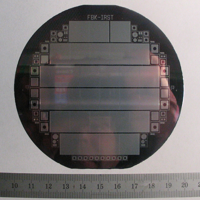
Figure 3.6 shows a partial view of the wafer. In the middle, two sensors for arranging six readout chips are visible. The vertical white lines correspond to two larger pixel () columns in the region where two readout ASICs will be arranged side by side.
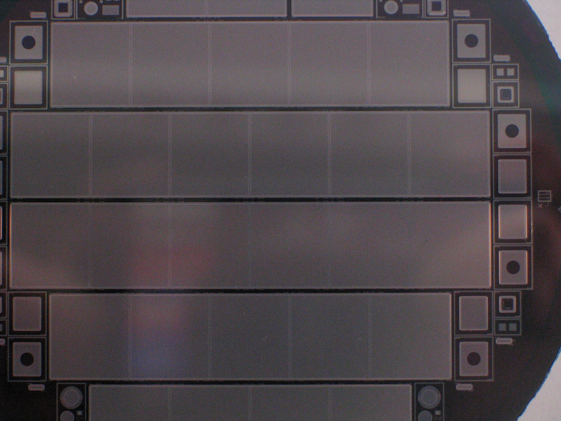
Figure 3.7 represents a partial view of a sensor made with pixels. At one corner of each pixel the pad for the bump bonding is visible. These are arranged in a mirror configuration with respect to a bus serving two pixel columns. The pitch along the column is 100 m, and along the rows is alternatively 50 m and 150 m.
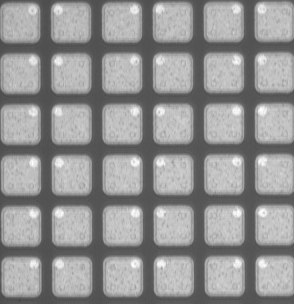
In these sensors the passive silicon edge housing guard
rings is 700 m wide (about 10% of the sensor size). The guard ring closest to
the sensor has a width of 100 m and it is connected to ground,
additional guard rings are floating.
This configuration has been applied as a preliminary
layout similar to the previous sensors designed for
LHC experiments. In our case the use of epitaxial silicon
sensors gives the possibility of a reduced bias voltage
during the sensor lifetime as a consequence of a lower full
depletion voltage. A limited guard ring
number reducing the previous passive silicon edge of 50%
could be possible. This evaluation has been obtained from
simulations carried out in collaboration with FBK, showing
the break down voltage as a function of the floating guard ring number.
Experimental measurement using the single chip assembly based on ToPix v3
will be performed to validate the simulation results.
Middle resistivity wafers used during the radiation
damage test have been investigated for
these tests.
Three epitaxial
thicknesses were chosen to better investigate the thickness
dependence during the thinning process. Epi-75
low resistivity wafers were added for comparison purposes.
Sixteen wafers were thinned at the Wafer Solution company:
the Epi-50 and Epi-75 wafers to the target of 100 m thicknesses
and the Epi-100 wafer to 120 m thickness,
in addition, half of these wafers were diced to obtain sensors.
No mechanical breakage occurred.
Tests
In addition to the radiation damage test of the epitaxial material used to make the first sensor prototypes with the results already described in the previous section, I-V and C-V measurements and planarity and thickness tests were performed.
In particular I-V and C-V measurements were made on some test structures before and after thinning and dicing of wafers to investigate potential mechanical damage in the bulk of the wafer. Variations within measurement errors have been reported in the I-V and C-V trends and no changes in the leakage current and full depletion voltage values were observed.
Concerning the planarity evaluation, two techniques were used compatible with the equipment at disposal at INFN-Torino: a Mitutoyo measurement machine equipped with both a precision CCD camera (magnifier 1:10) and a stylus probe (3 m over 1 m precision). Simply to put down the 4 inch thinned wafers on the measurement base and using a CCD camera, a total unplanarity of about 40% was measured by a grid of measurement positions and a preferential cup shape was observed. This result can be explained both with the elasticity of the wafer now thinned and a measurement imprecision due to the reflection of the light on the mirror like wafer surface.
By using the probe the elasticity of the wafer was immediately detected by observing the movement of the wafer under the probe pressure, without any breakage. The thickness measurement has been obtained using the same grid of 72 measurement positions as previously discussed. Figure 3.8 shows the result obtained for a 100 m thick nominal wafer.
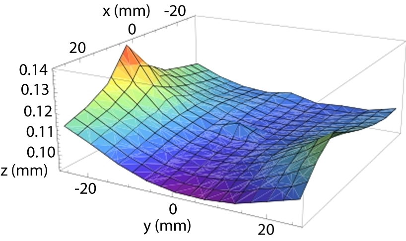
3.2.4 Technology Choice Epi vs. Oxygen
The higher radiation tolerance of the epitaxial devices in contrast to FZ ones can be explained taking into account the oxygen diffusion from the Cz substrate [oxygen0], as shown in figure 3.9.
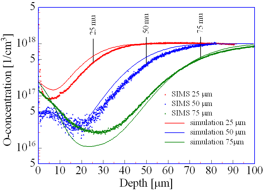
According to the oxidation process used to increase oxygen concentration in the FZ wafers [oxygen0] as shown in figure 3.10, some epitaxial wafers were submitted to an oxygen process at the FBK. In particular a 1100 ∘C phase for 12 hours with wafers in oxygen atmosphere was followed by a phase of 53.6 hours at 1100 ∘C temperature in a nitrogen atmosphere. Then SIMS measurements of the oxygen concentration as a funtion of depth were performed at ITME.
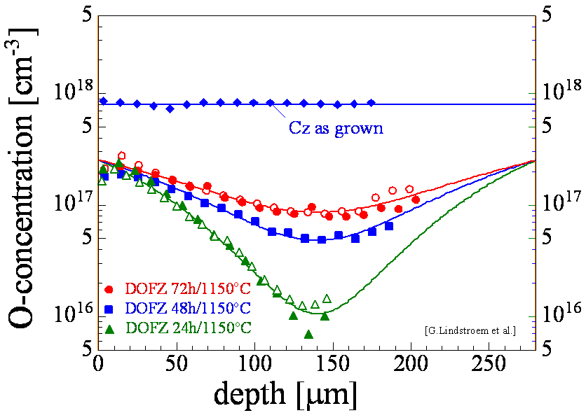
Figure 3.11 reports the result for an epitaxial wafer 100 m thick. The flat trend can be explained with both contributions coming from the Cz substrate oxygen diffusion and from diffusion from oxygen atmosphere during the high temperature phase. Such a result shows the possibility to have a uniform tolerance to the radiation along the sensor bulk.
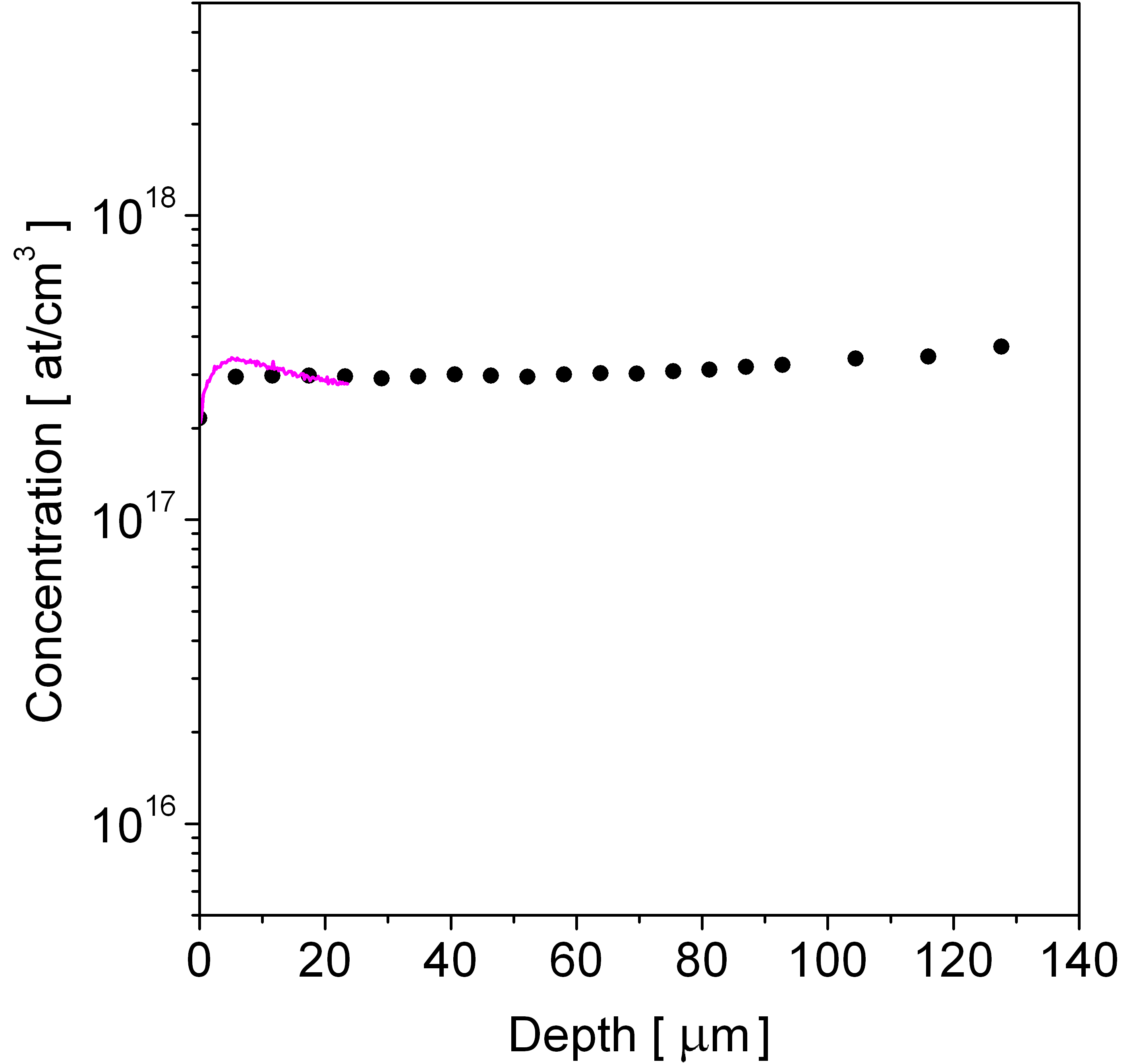
3.2.5 Production
Taking into account the first design of the full sensors for the pixel detector as reported in the drawing of figure 3.12 and the needed sensor number for making the whole pixel detector as reported in table 3.4 a minimum number of 34 wafers has to be produced. More details will be explained in the section 3.6.
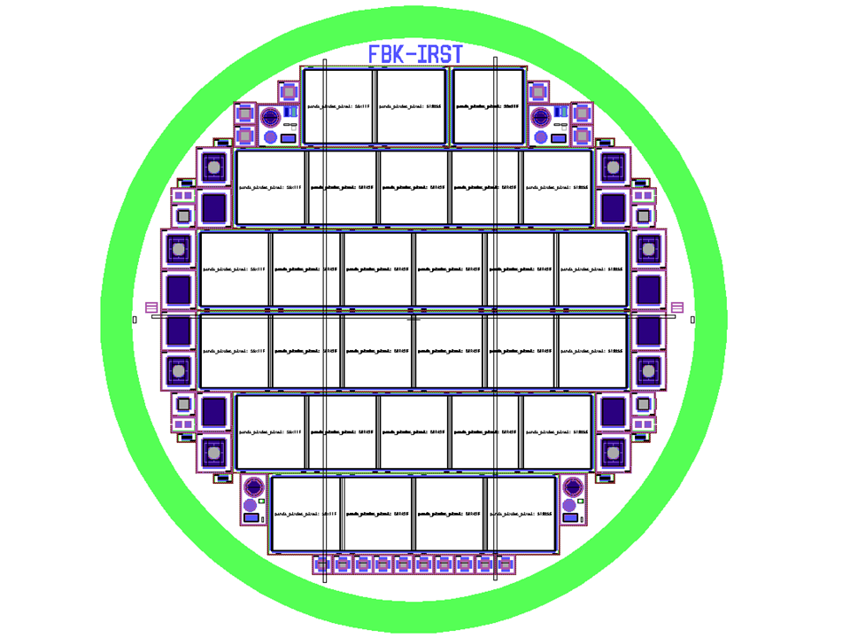
| S2 | S4 | S5 | S6 | Total | |
|---|---|---|---|---|---|
| Barrel1 | 6 | 8 | 0 | 0 | 14 |
| Barrel2 | 0 | 0 | 6 | 44 | 50 |
| Disk1 | 6 | 2 | 0 | 0 | 8 |
| Disk2 | 6 | 2 | 0 | 0 | 8 |
| Disk3 | 4 | 4 | 12 | 4 | 24 |
| Disk4 | 4 | 4 | 12 | 4 | 24 |
| Disk5 | 4 | 4 | 12 | 4 | 24 |
| Disk6 | 4 | 4 | 12 | 4 | 24 |
| Total | 34 | 28 | 54 | 60 | 176 |
| Chip Number | 68 | 112 | 270 | 360 | 810 |
In particular, quality control of each patterned wafer will be performed on test structures adjacent to the sensors: C-V, I-V trends on test diodes, C-V on MOS structure, I-V trend on a gated diode, breakdown voltage for several GR (Guard Ring) configurations, C-V interpixel measurement. Visual inspection of metals and bonding pads of each sensor can be planned for checking for example the etching uniformity. Doping profiles as a function of epitaxial depth and bias voltage are additional measurements useful to compare a wafer before and after the oxygen process. Besides, wafer samples from production processes will be used to obtain diodes for radiation damage tests to monitor the radiation resistance uniformity.
ITME has been selected as the company able to provide the epitaxial wafers useful for our project by checking samples during the R&D. FBK has shown the capabilities for sensor production.
In table 3.5 the most probable properties of the epitaxial wafer for the production are summarised.
| Cz substrate | |
|---|---|
| Diameter | mm |
| Orientation | |
| Conductivity type | |
| Dopant | Sb |
| Thickness | m |
| Resistivity | |
| Epitaxial Layer | |
| Conductivity type | n |
| Dopant | P |
| Thickness(centre) | m |
| Resistivity | |
3.3 Front-End Electronics
3.3.1 Requirements
The pixel readout ASIC has to provide for each hit a simultaneous position,
time, and energy loss measurement. The specifications for the readout
electronics depend on the requirements of the MVD. The fundamental parameters
to take into account are the \PANDAradiation environment and the close proximity
of the MVD to the interaction point.
A pixel size of has been chosen based on
the study of track performance. Since each readout cell has to be bump bonded to
the sensor, the readout cell matrix has to respect the same geometry as the pixel
sensor matrix. Therefore the readout cell has to fit in an area of
.
To guarantee the reliability of the system, time and charge
digitisation has to be performed at the pixel cell level in
order to transmit only digital information
out of the pixel cell. For a Minimum Ionising Particle (MIP)
in a 100 m thick epitaxial sensor an average ionisation charge of
1.3 fC is expected. The upper limit of the dynamic range is given
by the measurement of protons with a momentum down to
200 \mevc, which can deposit ionisation charges up to 50 fC.
A power density of up to can be tolerated.
However, a strong effort is going into the reduction of the power consumption
of the \frontendelectronics and hence the material budget for the cooling
system.
It is foreseen to employ a p-in-n epitaxial sensor, which should
give an adequate radiation hardness with a simple geometry. However,
the possibility of using the already well known n-in-n sensor employed in
LHC is considered as a backup solution. Therefore, the \frontendhas to be designed to be compatible with sensors of either polarity.
The noise level is mainly limited by the input transistor thermal
noise, and therefore
is a function of its bias current. An Equivalent Noise Charge (ENC)
of 200 electrons is a good trade-off between power consumption
and minimum detectable charge. The readout electronics has to work
in the \PANDAradiation environment, with an accumulated Total Ionising
Dose (TID) of 100 kGy in 10 years. Hit rate simulation studies estimate
an average rate of maximal events per second on a single pixel
cell. The system will be self-triggered and all the events above a given
threshold have to be read out, leading to a high data rate. A time
resolution lower than the average event rate of events/s is
required. Table 3.6 summarises the specifications for
the ASIC design.
| Pixel size | |
|---|---|
| Self trigger capability | |
| Chip active area | |
| 116 rows, 110 columns | |
| Chip size | |
| measurement | ToT |
| Energy loss | 12 bits resolution |
| measurement | 7 bits linearity |
| Input range | up to 50 fC |
| Noise floor | fC |
| Clock frequency | 155.52 MHz |
| Time resolution | 6.45 ns (1.9 ns r.m.s.) |
| Power budget | 800 mW/cm2 |
| Max event rate/cm2 | Hits/s |
| Max data rate/chip | Mbit/s |
| Total ionising dose | kGy |
3.3.2 Readout Architecture
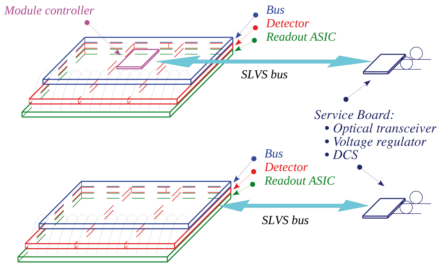
The readout architecture, depicted in figure 3.13,
foresees a module structure formed by a three-layer structure: the
sensor, the \frontendchip and the transmission bus. The sensor is
bump-bonded to the readout chips which, in turn are wire-bonded to the
transmission bus.
The module is connected to a service board, located outside the sensitive
area, which performs the data multiplexing and the electrical-to-optical
conversion to decrease the amount of cabling. The link is bi-directional
and allows to send the clock and to upload configuration parameters to
the \frontend. A second service board hosts the voltage regulators.
Due to the low power supply voltage of the \frontend(1.2 V), a
DC-DC down-conversion will be implemented at this level.
As shown in figure 3.13, two possible solutions are
under evaluation: in the first one, a module controller chip is used
on top of the transmission bus to receive, multiplex and re-transmit
the data from the \frontendchips over high speed serial links. In the second
solution the module is directly connected to the service board. The advantage
of the first solution is the reduction of the number of wires coming out the
module; moreover, by multiplexing the data from various \frontendchips, a
better bandwidth allocation is possible. On the other hand, when compared to
the second solution, it requires an extra ASIC which increases the power
consumption and becomes a critical point of failure.
3.3.3 Front-End ASIC
A new \frontendASIC, named ToPix, is under development in order to
cope with the unique requirements of the \PANDAexperiment.
The circuit is developed in a commercial CMOS 0.13 m technology, in
order to profit from the high level of integration and the intrinsic radiation
tolerance of deep submicron technologies. Indeed, it has been shown
[Faccio05] that deep submicron technologies with very thin gate oxide and
Shallow Trench Insulation (STI) have the potential to stand high levels of
total ionising dose with standard layout techniques. In order to cope with the
Single Event Upset (SEU) effect, all flip flops and latches in the pixel
cell are fully static and are based either on Hamming encoding or triple
redundancy.
Pixel Cell
In the proposed design, the Time over Threshold (ToT) technique has been adopted for the amplitude measurement. The ToT allows to achieve good linearity and excellent resolution even when the preamplifier is saturated, thus making room for a high dynamic range. Owing to the saturation of the input stage, a cross talk of the order of few percent is expected for large input charges. The ToT is obtained by taking advantage of the time stamp which is already distributed to all pixels in order to obtain the time information.
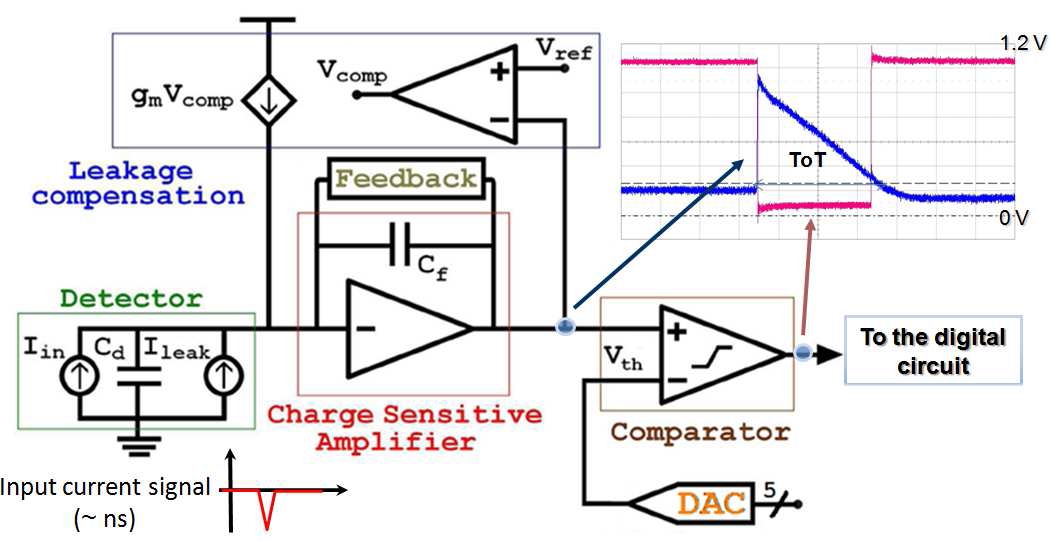
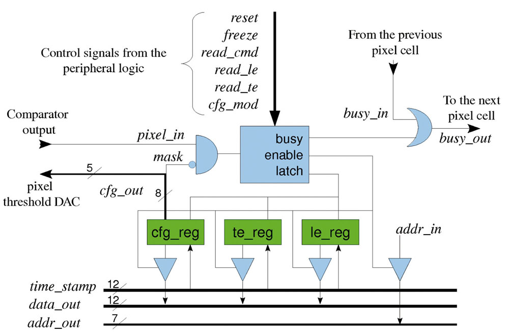
Figures 3.14 and 3.15 show the schematic
of the analogue and digital parts of the pixel cell, respectively.
The charge preamplifier is a gain-enhanced direct cascode amplifier with a
feedback capacitor and a constant current discharge circuit. A low frequency
differential amplifier in feedback with the input stage allows for
leakage current compensation by forcing the stage DC output value to
a reference voltage. The input amplifier can be configured to accept
signals of both polarities via control bits. A calibration signal can
be applied to the input of each preamplifier via a 24 fF integrated
capacitor. Each pixel can be independently enabled to receive the
calibration signal via the configuration register. The comparator is
based on a folded cascode architecture. The threshold voltage is set
by global DAC and can be fine adjusted via a 4 bits local DAC.
When the preamplifier output crosses a threshold, the comparator switches
to 1 and the time stamp value is loaded into the leading edge register. The
integrating capacitor is then slowly discharged and when the amplifier
output goes
below the threshold, the comparator switches back to 0 and the time
stamp value
is loaded into the trailing edge register. Therefore the time stamp
value in the leading edge register gives the timing information,
while the difference between leading and trailing edge time stamps
gives the amplitude information.
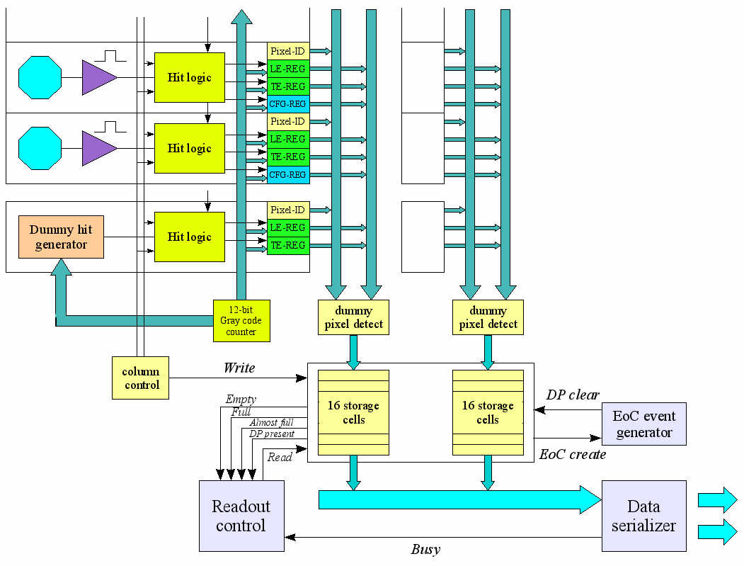
ToPix Architecture
The pixel cells are organised in double columns which share the same
time stamp and readout buses. Each double column is composed of
cells, a 12 bit time stamp bus, a 7 bit address bus
and a 12 bit data bus. Each cell in the column has
a unique cell address which is hardwired.
The readout buses are differential. The time stamp bus uses a reduced
swing pseudo differential logic with pre-emphasis to limit the power
consumption without degrading the speed performance. The time information
is sent on the bus with a Gray encoding to reduce the switching noise and
to avoid synchronisation problems with the asynchronous pixel logic.
The address and data readout buses are CMOS pseudo differential lines and
are read out at the end of the column via sense amplifier in order to keep
the cell output drivers to a manageable size and power consumption.
The column readout scheme is based on a concept similar to the one used
in other pixel readout designs [Peric06]. When a pixel cell receives
a hit it generates a busy signal which is put in logical OR with the busy
of the previous cell, and then sent to the next cell. Therefore at the end
of the column the busy signal is high if at least one pixel contains data.
The readout is made in a fixed priority scheme: the read commands are
sent to all pixels, but only the one with its busy input signal at zero
(i.e. with no pixel at higher priority with data) sends its data and address
to the output bus. A freeze signal is used to block
the generation of new busy signals (but not the possibility to
store an event into the pixel)
during readout in order to make sure that all the pixels are addressed
in a readout cycle.

The configuration data upload uses the same scheme: the config mode
signal puts all pixels in
the busy state. Successive commands address the pixels from the one
with highest priority
to the one with the lowest. During each address phase, it is possible
to write the data on
the time stamp bus (now used to send configuration information and thus not connected to the
counter) in the configuration register or to put the data stored in
the configuration register
on the data bus.
Each double column is controlled by a Column Readout Control Unit (CRCU). The
CRCU consists of four main components: a bank of differential drivers for the
time stamp propagation, a bank of sense amplifiers for the data readout, a
32 cells output FIFO and the control logic. The CRCU sends the readout
signals on the base of the state of the busy from the pixel column and the state
of the output FIFO.
The ToPix readout is controlled by a Chip Controller Unit (CCU), which reads
the data from the 55 CRCUs and multiplexes them to up to 3 double data rate
serial links. The multiplexing operation is made in a round robin scheme with
two queues, a fast one for the CRCU FIFOs with less than 5 free cells and a
slow one for the others.
Data are transmitted in frames. A frame contains all the data received by
the chip during a single time stamp counter cycle. Each frame is divided from
the previous and the next ones by a header and a trailer, respectively. Figure 3.17
shows the frame structure.
Frames are composed by 40 bits wide words with a 2 bit header to identify a data word from a header or a trailer word. The data word contains 14 bits for the pixel address and 24 bits for the leading and trailing edge time information. The header word contains the chip address, the frame counter and error detection and correction bits. The trailer word contains the number of words present in the frame, the Cyclic Redundant Check (CRC) of the entire frame and the error detection and correction bits.
3.3.4 Module Controller
One of the two readout options for the pixel sensors shown in figure 3.13
foresees a module controller ASIC located on the module structure. The use of
a module controller has been a common choice in the electronic readout of the LHC
pixel detectors [Beccherle02][Schnetzer03][Kluge07], because it gives
a greater degree of flexibility.
In the \PANDAMVD readout scheme the use of a module controller would allow a
reduction of the transmission lines by using a Phase Locked Loop (PLL) and therefore the possibility
to transmit data at a bit rate faster than the clock frequency. Moreover, it would
also allow a better load balancing between \frontendchips with high and
low event rates.
However, the disadvantages in terms of higher power consumption, increased number of
cooling pipes and increased system fragility due to the introduction of a critical
single point of failure makes the solution without module controller more attractive.
3.3.5 ASIC Prototypes
An R&D activity for the design of the ToPix ASIC is ongoing. In the following the three ToPix prototypes will be described, together with the test results.
ToPix Version 1
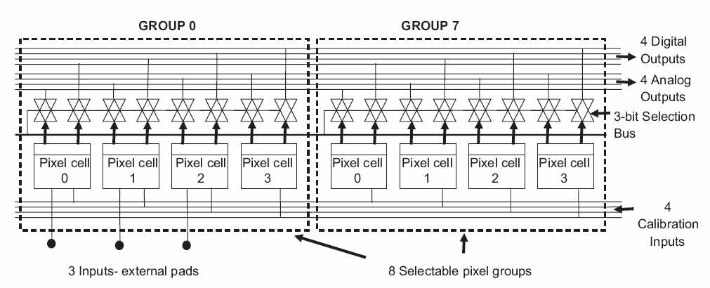
A small prototype with the basic pixel cell building blocks was designed in order
to evaluate the analogue performances and gain experience with the technology.
This first prototype [Calvo08] chip contains 32 readout cells,
each one equipped with a preamplifier and a discriminator. The preamplifier consist
of a Charge Sensitive Amplifier (CSA) with a feedback capacitance of 10 fF, a
constant current feedback and a baseline restorer. The amplifier size is
and the discriminator size is . Figure 3.18 shows the ToPix v1
architecture. The ASIC size is . The cells are arranged in
8 groups of 4 cells. Each group has 4 calibration input lines, 4 analogue output
lines, and 4 digital output lines.
Each input calibration line is in common for one of the cells in each of
the 8 groups. In each cell, a calibration capacitor of 30 fF shunts the
calibration line to the input node. Therefore, sending a voltage step on
the calibration line a delta shaped current pulse is injected at the input node.
The output lines are multiplexed in order to be shared between the cells belonging
to different groups. In order to drive the capacitive load of output pads and
measurement probes, which can be up to 10 pF, the analogue signals are driven by
a source follower and the digital signals are driven by a buffer. Six cells
belonging to two different groups have direct connection to dedicated input pads.
This configuration allows the observation of the cross-channel effects.
Figure 3.19 shows a simplified schematic view of ToPix v1 readout, which is designed to work with an n-type sensor (negative current pulses). The CSA core amplifier has three feedback components:
-
•
The feedback capacitance fixes the charge gain (1/). On the one hand a high value of decreases the CSA charge gain, on the other hand a low value of decreases the CSA loop stability. In this prototype a nominal value of the feedback capacitance of 10 fF has been chosen as the optimal compromise between gain and loop stability.
-
•
The baseline restorer is implemented with a low pass filter stage which computes the difference between the baseline reference voltage and the CSA output. The resulting low frequency voltage signal controls the gate of a PMOS which generates the leakage compensation current at the input node.
-
•
The discharging current generator is based on a differential pair. The two inputs are connected to the CSA output and to the baseline reference voltage, respectively. The differential pair is biased by a current source. When the current is equally shared in the two branches of the differential pair. When a negative current signal is present at the CSA input, increases, thus switching off one of the two branches. Consequently the current flows in the input node and is discharged. A good constant discharge is achieved only when is sufficiently large to fully steer the current from one branch to the other of the differential pair. Since the two transistors at the differential pair input work in weak inversion this voltage is about 40 mV.
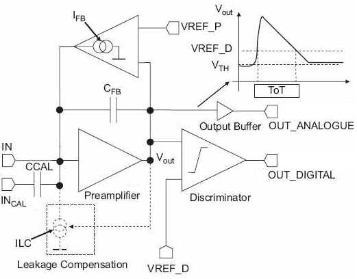
The constant current discharge provides a constant slope trailing edge of the preamplifier output signal which, in turn, provides a linear ToT measurement of the sensor charge signal.The discharge current source () is normally turned off. When an input signal is applied, the output voltage of the preamplifier increases very fast, exceeding the voltage VREF_P, the current source is turned on and the feedback capacitor is discharged with constant current until equilibrium is restored, and the output level of the amplifier turns back to VREF_P. The dynamic range is extended by discharging the feedback capacitor at the input node, preserving the linearity of the ToT measurement even for higher input signals, when the preamplifier output is saturated. The feedback topology considered is similar to the one employed in [Peric06]. The discriminator design follows a low-voltage approach employing a single stage folded-cascode topology followed by two inverters. For test purposes each channel is provided with an internal calibration capacitor driven by an external signal , with amplitude . The injected charge is given by the product . The absolute value of is known with an accuracy of 10%.
ToPix Version 1 Test Results
Figure 3.20 shows a typical pulse at the output of the preamplifier for an input charge signal of 0.5 fC, measured with an oscilloscope and a differential probe, for best common mode noise rejection. The preamplifier gain in the linear region is 60 mV/fC. This value was obtained fitting 5 calibration points with nominal values of 1, 3, 4, 8, 12 fC. The r.m.s. output noise is 1 mV. Assuming a gain of 60 mV/fC this translates to an equivalent input noise of 100 e- rms. The power consumption is 12 W per pixel cell using a 1.2 V power supply. The test results are summarised in table 3.7.
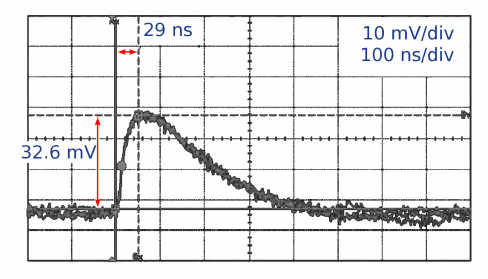
| analogue gain | 60 mV/fC |
|---|---|
| Linear input gain | 100 fC |
| () | 1 mV |
| ENC () | 104 e- |
| Power consumption | 12 W/cell |
| ToT dispersion (rms) | 20% |
| Baseline dispersion (rms) | 13 mV |
ToPix Version 2
A second prototype of the ToPix ASIC has been designed and tested in order to prove the pixel cells and column functionality. This chip is designed for a clock frequency of 50 MHz as in the original specifications.
The prototype includes two 128-cell and two 32-cell columns. The pixel cells include all the functional blocks required for the final ASIC except for the bonding pad opening. The end-of-column logic has been greatly simplified for test purposes and includes only the counter and the bus readout sense amplifiers. The prototype block diagram is shown in figure 3.21.
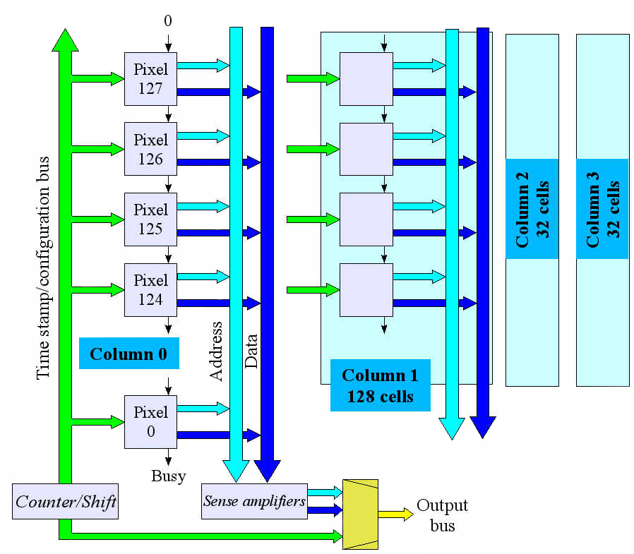
The chip has been designed in a commercial CMOS 0.13 m technology with 8 metal layers. The two 128-cell columns are folded in four 32-cell slices in order to have an acceptable form factor. This arrangement represents a worst case with respect to the final floorplan because of the longer interconnections. The die size is . Figure 3.22 shows the chip die.
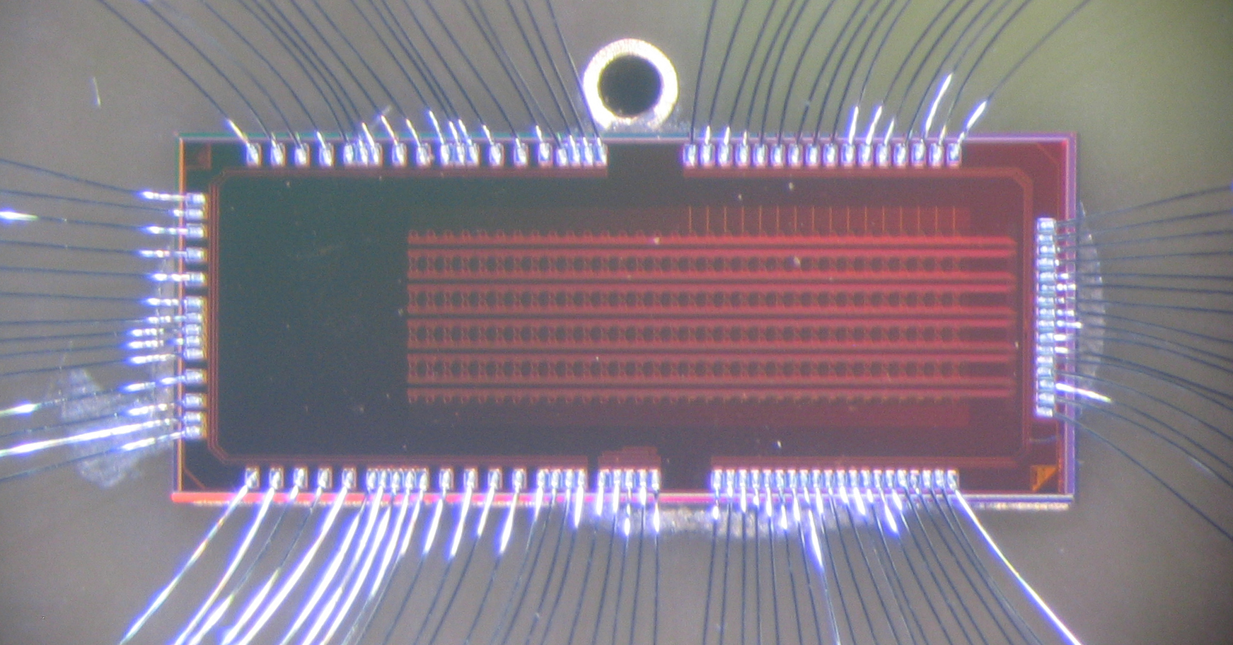
The Single Event Upset (SEU) effect has been mitigated by designing
all flip flops and latches in the pixel cell as fully static and based on
the DICE architecture [Calin96]. This architecture, shown in
figure 3.23, is insensitive to SEU as far as only one circuit
node received the voltage spike due to the incoming particle. The area
penalty is about a factor of 2, compared with the factor of a triple
redundancy circuit.
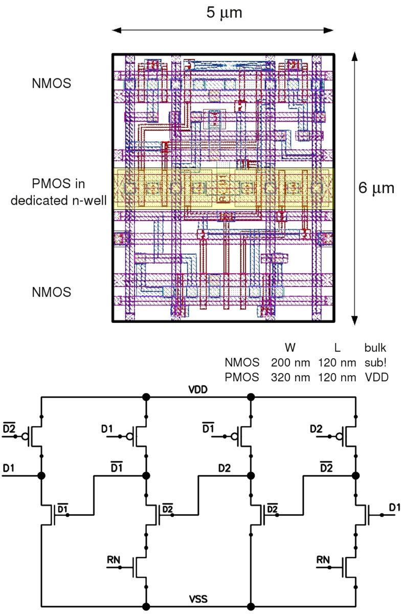
A number of features has been added in order to improve testability. In addition to the internal charge injection circuit, the inputs of 16 cells of the first column are connected to an external pad. It is therefore possible to connect the chip to a detector in a simple way. The drawback of such an arrangement is that it leads to a significant increase of the input capacitance and therefore of the noise. All digital control signals are provided externally, in order to allow testing and optimisation of the speed and synchronisation of the readout sequence. It should be noted that the folding configuration is a slightly worse case with respect to the timing because of the longer bus lines.
ToPix Version 2 Test Results
Test of the ASIC was performed with a DAQ chain based on a NI-PCI (National Instruments) system using the PCI-7831R board and LabVIEW software. The NI-FPGA generates pattern and works as a triggered memory. A Virtex II FPGA shifts voltage levels. To allow the test of ToPix v2 with a 50 MHz clock, a setup with a bidirectional FIFO has been implemented on the FPGA board, see figure 3.24.
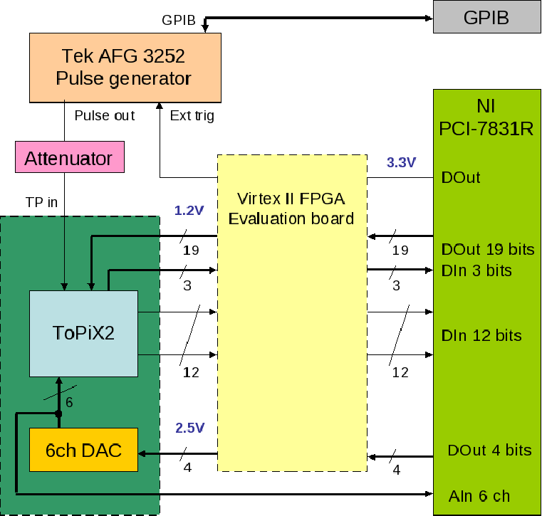
The prototype has been tested both by injecting charge through the inputs connected to the pads and through the internal calibration circuit. Figures 3.25 and 3.26 show the input-output transfer function and the linearity over the whole dynamic range for two typical pixels.
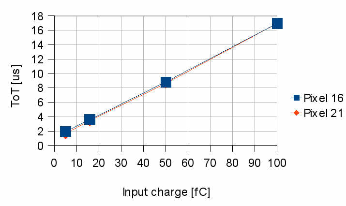
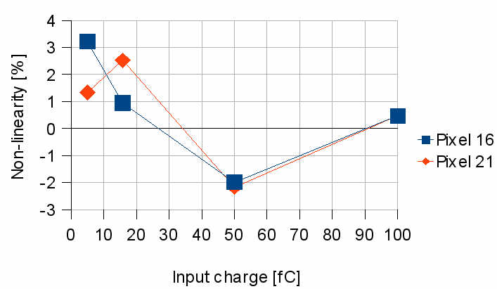
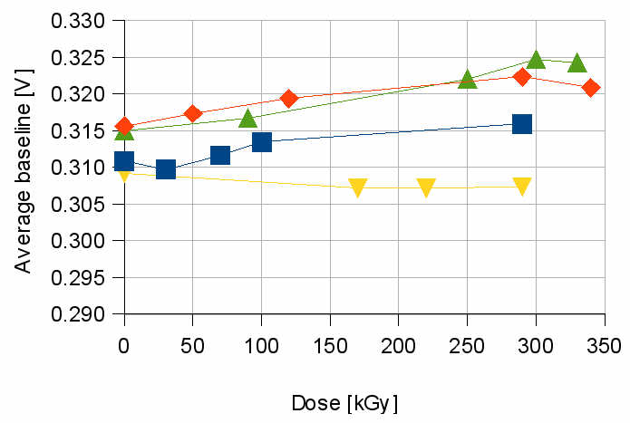
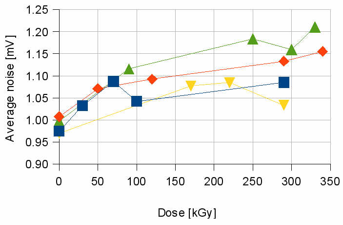
Total dose irradiation tests have been performed on four chips with a rate of 4.07 Gy/s. Figures 3.27 and 3.28 show the average of the baseline and the noise over some of the 320 cells of 4 chips during irradiation, obtained with a threshold scan in order to remove the quantisation error. The baseline variation is below 3% and is comparable with the dispersion due to the process variation. The noise level is around 1 mV r.m.s. before irradiation, which corresponds to 0.025 fC. An increase of 20%, to 0.03 fC, has been observed after irradiation. The measured noise value if higher than the 0.017 fC measured for the first ToPix prototype. It should be considered that in the ToPix v2 a large metal plate has been connected to the pixel input to emulate the bonding pad capacitance. Simulations show that the capacitance added by the metal plate justify the noise increase.
After irradiation the chips have been annealed at 100 ∘C. Figures 3.29 and 3.30 show a partial recovery in the baseline value and an almost complete recovery of the noise level to the pre-irradiation values.
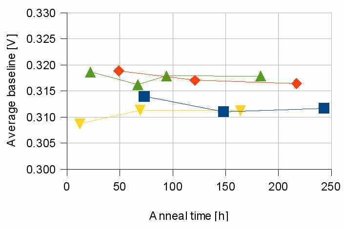
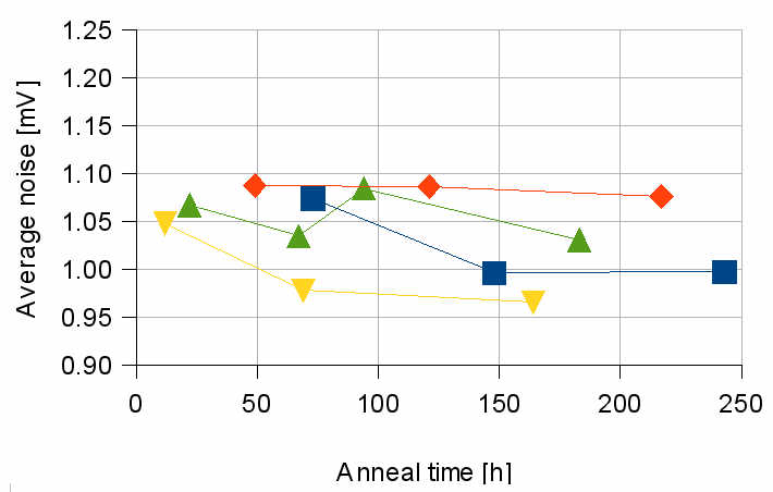
Figures 3.31 and 3.32 show the average and tail slope during irradiation. In this case the variation is much more relevant, up to 2 times in case of the average and up to 6 times for the . The problem lies in the very small current (around 6 nA) required to discharge the integrating capacitor to obtain the required resolution. With such low currents the leakage current induced by radiation plays an important role.
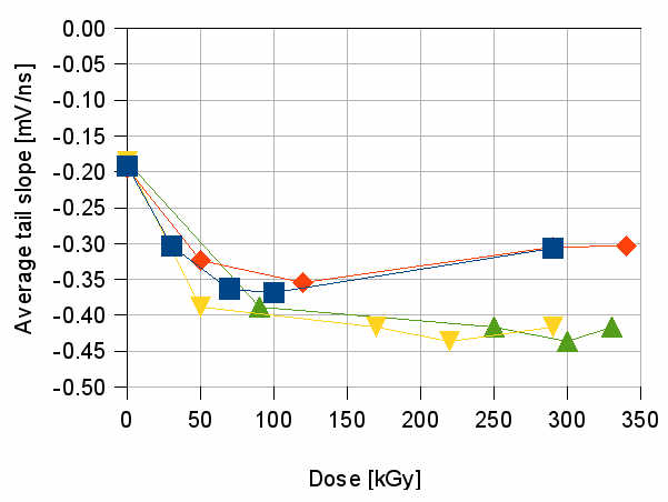
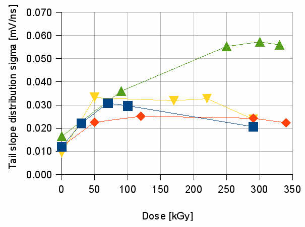
A possible solution is to use an enclosed gate layout for the critical transistors of the discharge circuit. Such a layout technique has been proven to be effective in preventing radiation-induced current leakage [Anelli99]. However, irradiation tests made on a previous prototype of the ToPix analogue part [Calvo08] showed that at dose rate of 0.011 Gy/s the relative ToT variation decreases by an amount between 22% and 54% in comparison with the variation after a dose rate of 4 Gy/s.
SEU Study
A dedicated study of the SEU in ToPix v2 has been performed in order to
verify if the DICE architecture was sufficient in the expected \PANDAenvironment.
To this aim the device has been tested with heavy ions at SIRAD (LNL-INFN)[sirad], and the convolution of
the experimental results with simulation studies allowed to estimate the maximum SEU rate of ToPix v2 in \PANDA(see [PANDAnote8]).
More ions of different energies, see table 3.8, have been used in order to have a wide range of
deposited energy.
Moreover it was
possible to investigate the deposited energy due
to different incident angles, rotating the support of ToPix v2 [angolo].
The irradiation runs lasted about 20 minutes and before and after
each run dosimetry measurements were carried out.
| Ion | Beam Angle | [MeV] | [MeV] |
|---|---|---|---|
| 16O | 101 | 0.70 | |
| 16O | 101 | 0.81 | |
| 19F | 111 | 0.91 | |
| 19F | 111 | 1.07 | |
| 28Si | 146 | 2.40 | |
| 35Cl | 159 | 3.01 | |
| 58Ni | 223 | 6.47 | |
| 79Br | 215 | 8.96 |
The study of the configuration register was performed using a control program developed with the LabView software, that wrote a 12 bit sequence of alternated 0 and 1 every 2 seconds and counted whenever some bits were changed. Knowing the number of SEUs () and the total incident particle fluence (), it is possible to calculate the probability to have an upset, usually called SEU cross section:
| (3.1) |
The has been calculated as the average of the cross sections coming from the several irradiation runs
with the same ion species,
and the standard deviation was used as an estimation of the error.
The experimental cross sections obtained have been fitted by a Weibull function (see figure 3.33)
It has the form:
| (3.2) |
where W and s are shape parameters. Here the s parameter was set to 3.
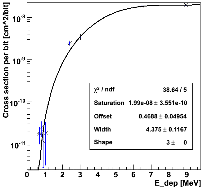
Our fit parameters for the configuration register, see figure 3.33, are:
-
•
=0.4688 \mev
-
•
[ ]
-
•
\mev
To evaluate the SEU rate of electronics developed in a standard layout without DICE architecture, two other components of the end column circuit
of ToPix v2 were tested for
irradiation.
The 12 bit shift register was tested using a method similar to the previous one (for the configuration register).
The 12 bit counter was tested with
a software comparing at fixed time intervals its value with the one of a “mirror” counter.
All the SEU tests were performed with a 10 MHz clock, although the nominal clock
of ToPix v2 is 50 MHz, because of the long cable of the setup.
The obtained fit parameters, see table 3.9, in these cases are very different from the Weibull parameters obtained from the
test of the configuration register. In particular the energy threshold is practically zero, this means that even a small deposited energy can
trigger an upset. The saturation cross section is bigger by a factor 2, in agreement with the fact that a higher SEU rate is expected in
electronics
designed in this standard layout.
| Device | [MeV] | [ ] | W [MeV] |
|---|---|---|---|
| SR | 1.03 | ||
| CNT | 1.46 |
In order to obtain the SEU rate, it is necessary to know the probability for a certain particle to deposit a certain energy in
the sensitive volume.
Following the procedure explained in [faccio_seu], the rate of SEU for the \PANDAhadron flux has been calculated, taking the lepton contribution to be negligible.
The evaluated SEU cross section in the hadron environment for the three tested elements of the ToPix v2 prototype,
has to be corrected with a 30% safety factor
to take into account
the under-estimation of the sensitive volume of 1 m3, as explained in [faccio_seu].
The calculated s are reported in table 3.10.
| [/bit] | ||
| CR | SR | CNT |
Multiplying the cross section by the hadron flux, obtained from a dedicated particle rate study [PANDAnote7], the SEU rates for annihilations on protons and on nuclei are obtained. The results are reported in table 3.11.
| Annihilation | CR | SR | CNT |
|---|---|---|---|
Taking into account the final design of ToPix, the SEU rate /h can be derived, taking into account that there are 12760 pixels, the 8 bits for the configuration registers and the 12 bits for the shift register and the counter. The estimated rates are listed in table 3.12. Considering the total number of chips (810) in the MVD pixel part, we can estimate about 2430 upsets per hour. The SEU rates foreseen for the shift register and the counter are higher in comparison to the configuration register as expected.
| Annihilation | CR | SR | CNT |
|---|---|---|---|
| 3 | 130 | 207 | |
| 1 | 27 | 42 |
The variation of one bit in the digital circuitry (SEU), following the passage of a particle, can be problematic in the \PANDAenvironment. The corruption of the data is not a dangerous effect in itself, because the corrupted data can be easily identified and discarded. Instead a more dangerous effect is the loss of the detector control function that can be restored resetting or rewriting the chip. As a consequence all the data stored from the upset event to the reset operation have to be discarded. As shown there is a relevant different SEU rate between a radiation tolerant architecture such as the configuration register of ToPix v2 and the non-radiation tolerant architecture, e.g. the shift register and the counter. Hence triple redundancy architecture application has been designed for the ToPix v3.
ToPix Version 3
A third prototype of the ToPix chip, designed to work with the 155 MHz clock updated to the new specifications, has been designed and tested. The prototype includes two cell and two cell double columns. The die size is . Bump bonding pads have been used in the pixel cells for direct connections to the detector. The 128 cells columns have been folded in four 32-cells sub-columns in order to have an almost square form factor, thus simplifing the die handling. The complete pixel cells and the end of column control logic and buffers have been implemented, while the output multiplexer and serialiser is still in a simplified revision. The chip layout is shown in figure 3.34.
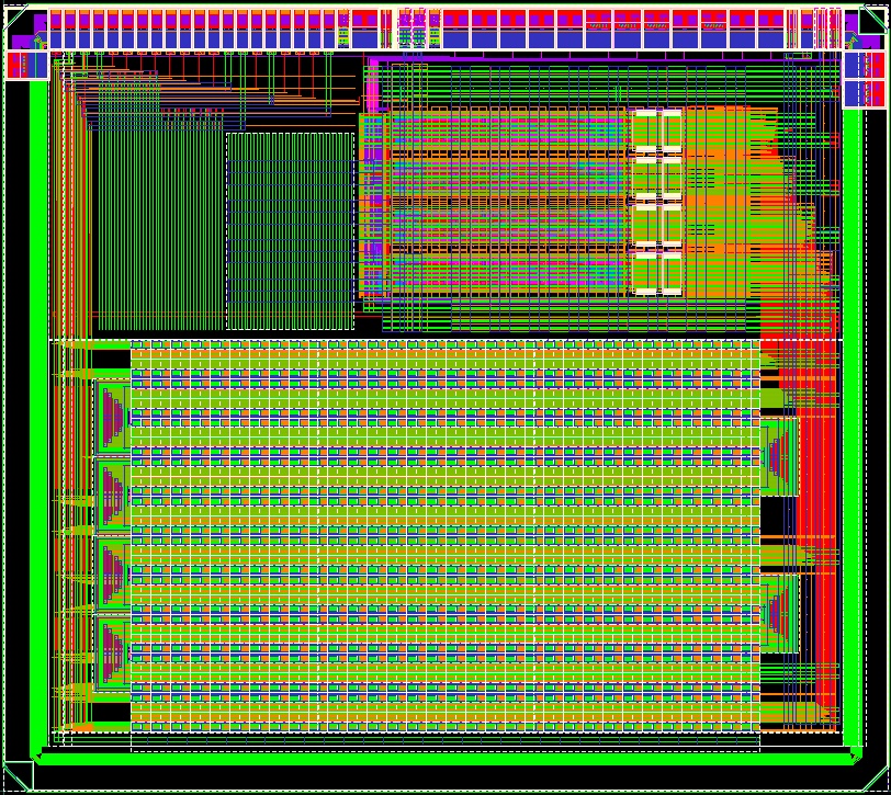
In this prototype a clipping circuit has been implemented in
order to avoid long dead-times for large input charges. The circuit forces a ToT
saturation at 16.5 s
while keeping a good linearity for charges up to 50 fC.
All flip flops in the pixel cell are fully static and use
the triple redundancy technique
in order to make them more SEU tolerant. The configuration
register implements an asynchronous
error detection and self-correction circuitry while the
leading and trailing edge registers
implement only the majority voter to save area. Therefore
the error correction works only
in the readout phase. In order to fit in the pixel area
the configuration register has been
reduced from 12 to 8 bits.
The chip is powered by a single 1.2 V power supply.
Digital input and output drivers
use the differential SLVS standard [SLVS] in
order to reduce the digital noise
contribution and to be compatible with the 1.2 V power supply.
Simulations with layout parasitic extraction and process
and mismatch variations show a gain
of ns/fC at mV and a
channel to channel ToT spread of 7%.
The simulated noise level is 155 e- at and
209 e- at nA.
The Analogue Cell Layout is implemented in an area of . The floorplan has been optimised in order to place the comparator between the most sensible analogue blocks (preamplifier, constant current feedback and baseline holder) and the digital cell. In figure 3.35 the different components of the analogue cell are shown.
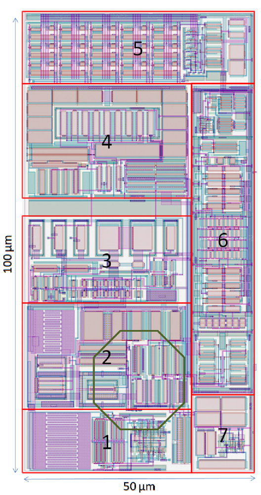
Charge Sensitive Amplifier
The bias lines are propagated vertically, low levels metal are employed for the bias line and high levels metal for the power supply lines.
In order to avoid the propagation of spurious signals through the power supply, 7 separate lines have been employed.
The input cascode stage of the CSA has a dedicated ground (gnd_pre).
The triple well transistors of the input stage have a dedicated supply net (vdd_pre) as shield.
The leakage compensation stage bias is given by vdd_ilc.
The comparator has a dedicated supply line (vdd_d) and a dedicated ground (gnd_d).
All the other analogue blocks are supplied by vdd_a and gnd_a.
The input stage is a gain enhanced cascode amplifier with capacitive feedback .
A feedback capacitance of 12 fF, which is half of the one employed in ToPix v2, has been chosen as the best compromise between the need of maximising the gain for low signals and the one of having an adequate phase margin in the feed-back loop. The output stage is a source follower which is employed as a voltage buffer to drive the output capacitive load. The schematic view of this stage is shown in figure 3.36.
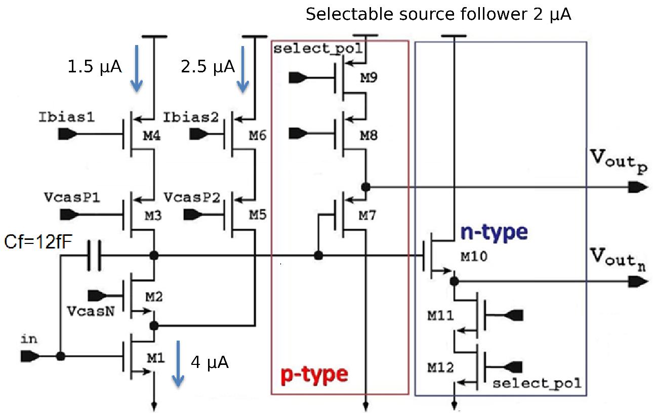
The chip will be produced in a p-substrate process, therefore the standard NMOS transistors are fabricated directly on the chip substrate. The process offers also the possibility of implementing the NMOS devices in dedicated wells (triple well option) as sketched in figure 3.37. In this case a deep n-well is fabricated in which the p-well hosting the NMOS transistors is put. This solution allows a good shielding of the transistor from the common chip substrate at the expense of an increased area. In a mixed mode design it is very important to protect the sensitive nodes from the potential interference of the digital switching circuitry. The triple well solution has hence been used for the input transistor M1 and its cascode device M2.
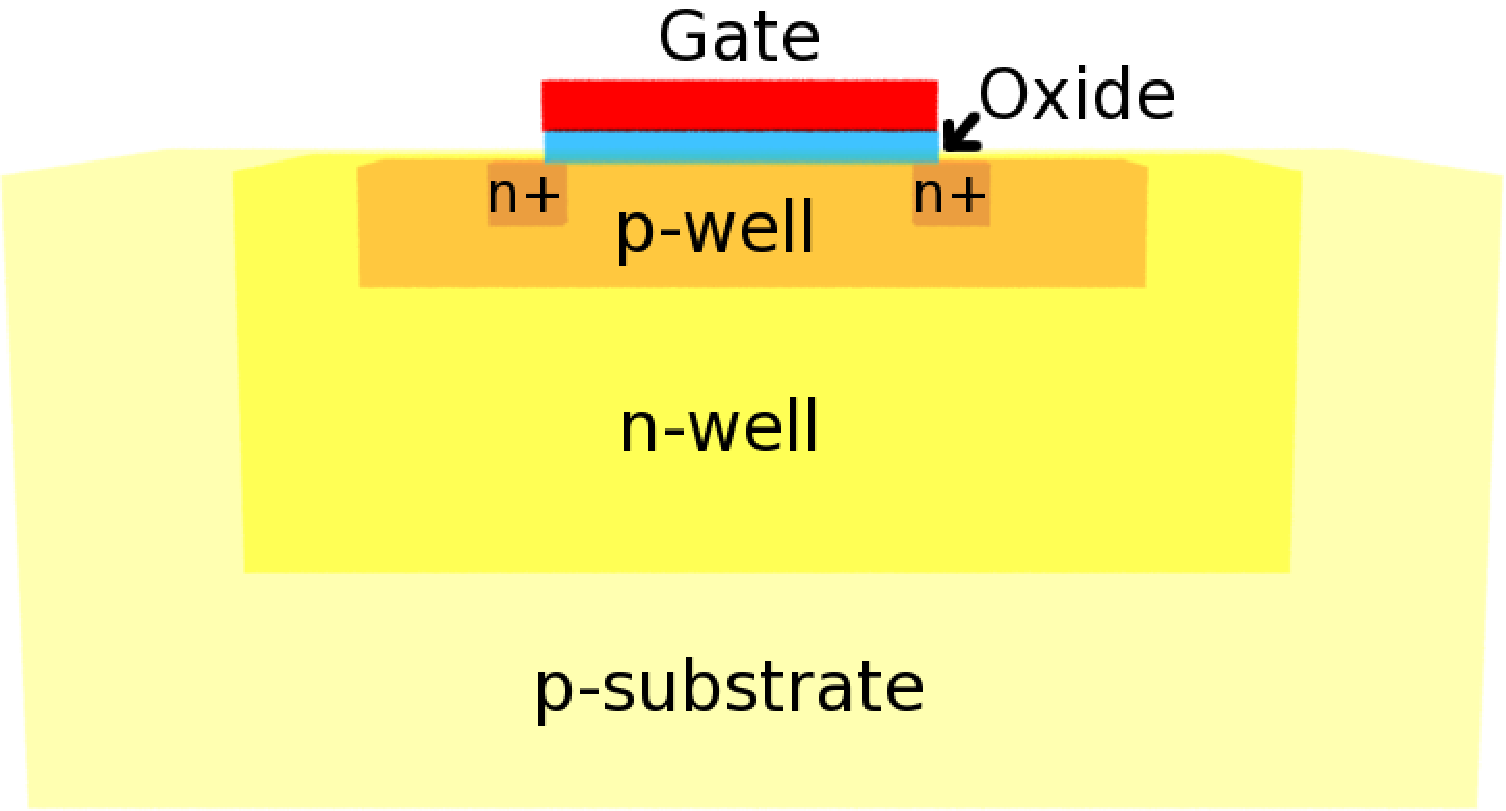
The CSA output stage is a source follower, which is employed as a voltage buffer to drive the loading capacitances at the input of the feedback stages and of the comparator.
Since the source follower has asymmetric rise and fall times and the polarity of the injected charge determines the direction of the leading edge, a NMOS source follower is needed for n-type sensors and a PMOS one for p-type sensors, hence maximising the output swing. The selection between the two is done via the select_pol status bit.
In p-type configuration select_pol is low, M9 is switched on and M12 is switched off.
In n-type configuration select_pol is high, M12 is switched on and M9 is switched off.
This stage is biased with a nominal current of 2 A.
The output DC voltage is regulated by the baseline holder. The value of the baseline voltage V_ref must be set according to the sensor type. Typical values are 300 mV for n-type sensors and 700 mV for p-type ones.
The buffers have the source and bulk short circuited in order to
suppress the bulk effect that would decrease their voltage gain. For
this reason transistor M11 in figure 3.36 is implemented
as a triple well device in order to decouple its bulk from the global
substrate and to allow the source-bulk connection.
Baseline Holder
The baseline holder is a specific feedback network that controls the DC output of the preamplifier, making it insensitive to the sensor
leakage current.
As a first step the solution presented in [Krummenacher91] has been considered for the leakage compensation.
A similar circuit has been designed in the current technology with a filtering capacitance of 10 pF in order to
evaluate
its leakage compensation capabilities. This filtering capacitance requires an area of about 500 m2,
which is close
to the maximum area that can be allocated for that component. The simulation results gave a ToT compression of
13%
for a 10 nA leakage current and of 38% for a 50 nA current. Therefore a different approach, based on a dual
feedback
loop has been preferred. This novel approach, shown in figure 3.38, is based on the fact that
in deep submicron
technologies MOS transistors with can provide a resistance in the G range.
Thanks to the high value of the equivalent resistance, a capacitance in the order of 5 pF is sufficient
to achieve a filter cut off frequency in the order of 10 Hz. The filtering capacitor is implemented
through MOS devices exploiting the gate oxide, and it occupies an area of 172 .
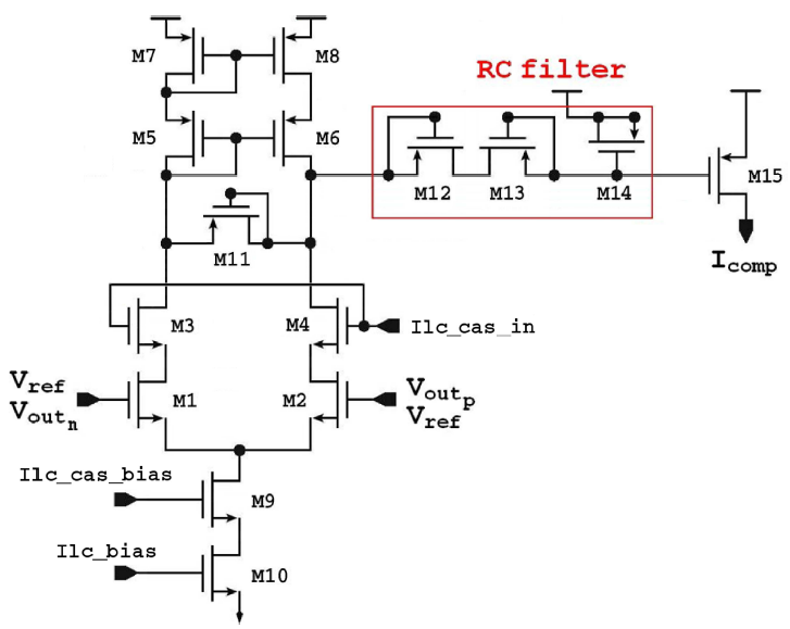
The output of the CSA is sensed by a differential pair and compared to the preset reference voltage.
The resulting error signal is used to drive a PMOS, which acts as a
voltage controlled current source and injects the compensation current
into the input node.
Constant Feedback Current Generator
The constant current feedback generator is a network that provides
the CSA discharging current [PericThesis].
Figure 3.39 shows the schematic view of this stage.
The CSA output signal is presented to the gate of M2, while M1 receives the baseline reference voltage.
With a p-type sensor, will have a negative polarity, steering all the current from M1 to M2. In this case the current in M3 is used to recharge the feed-back capacitor.
With n-type sensors, will be positive, steering the current from M2 to M1. M1 will have an excess current that will discharge the feedback capacitor.
At the equilibrium this stage provides an equivalent small signal feed-back resistance of 6.7 M with nA.
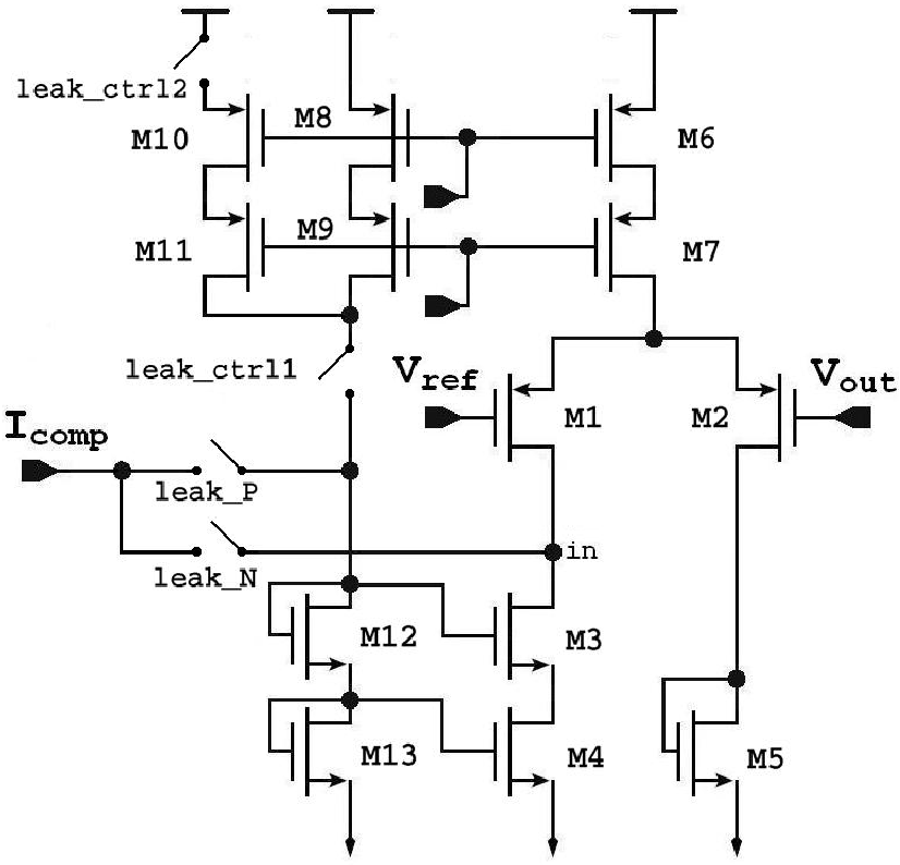
This stage provides also the injection of the leakage compensation current at the input node.
Using four switches it is possible to change the topology of the
circuit in order to choose the polarity of the current to be
compensated.
ToT Linear Range Limitation
When the CSA saturates the input node rises (p-type case) or drops (n-type case).
In both cases when the transistors connected at the input node are pushed out from the saturation region,
the discharging current increases leading to a compression of the ToT signal. This phenomenon depends on the
input capacitance and the input DC voltage.
Since the input DC voltage is at mV, assuming a detector capacitance of 200 fF, for an n-type sensor
the compression occurs from fC.
For a p-type sensor a much larger current ( fC) could be
collected on the input capacitance while ensuring the proper bias of
the constant current feedback.
Comparator
The comparator has a folded cascode input stage, and two CMOS inverters in cascade as driver in order to have a fast transition between the two logic states.
Since the comparator performance in ToPix v2 was satisfactory, the
transistor level implementation has not been changed. However the
layout has been redesigned in order to fit in the available cell area.
Figure 3.40 shows the transistor level implementation. The comparator gives a high level output when .
Therefore in n-type configuration, where the CSA output is positive, in1 is connected to the comparator reference voltage and the CSA output to in2. In p-type configuration where the CSA output is negative the signals are exchanged using CMOS switches.
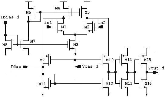
DAC Current Source
Since Vref_d is common to all pixels, in order to mitigate the
threshold dispersion a local 5 bit DAC is added in each pixel, to
allow a fine tuning of the threshold on a pixel by pixel basis.
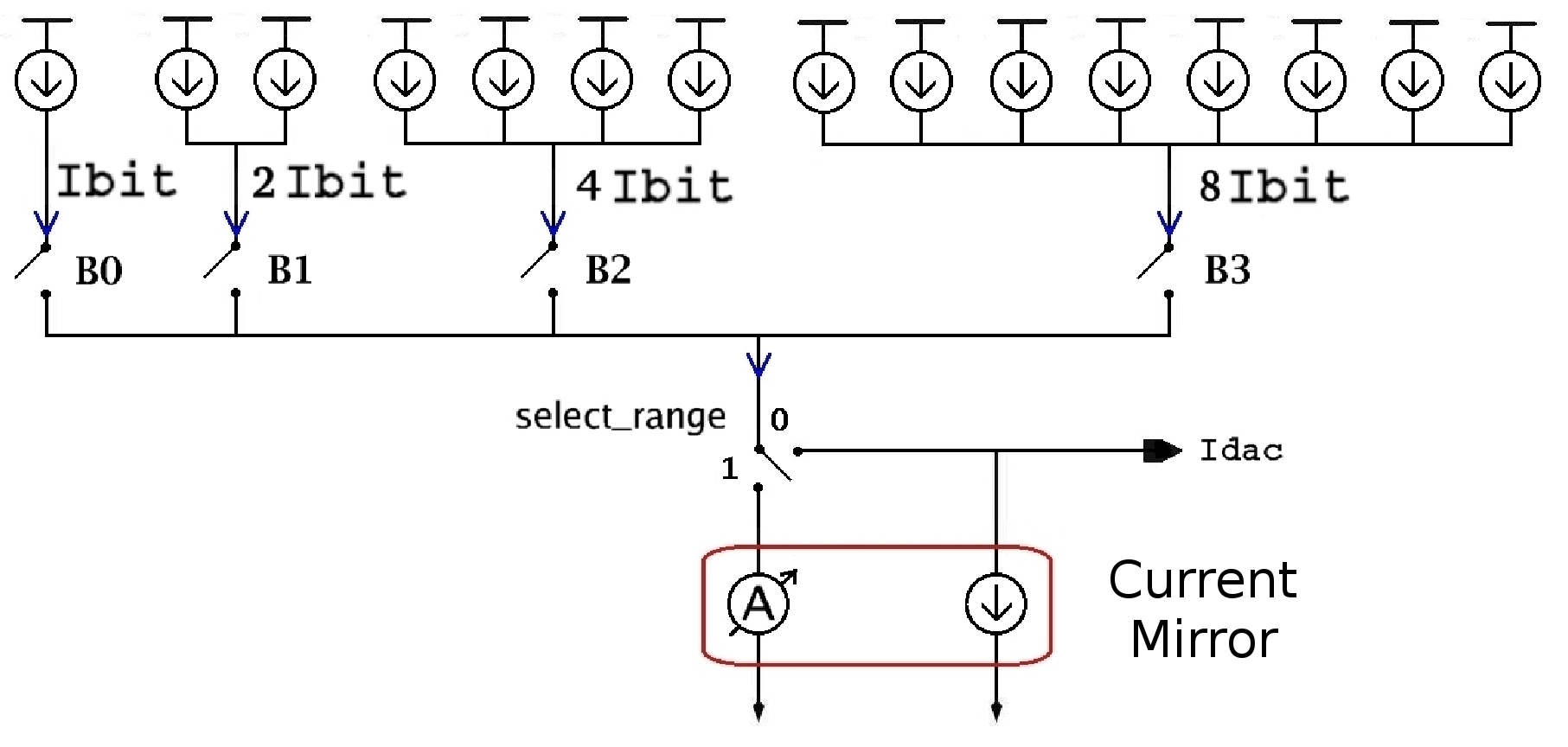
A simplified scheme of the DAC is shown in figure 3.41. For simplicity the switches are represented in common for each group of Ibit current generators.
Each of the bit B0, B1, B2, B3 controls a switch that activates the relative current generator.
Clipping Circuit
A clipping circuit has been designed in order to protect the \frontendwhen a large charge is presented at the input node, thus avoiding long dead times.
The \frontendrequires to measure charges up to 50 fC, so larger charges have to be discharged with an extra current.
The clipping circuit exploits the fact that the input node rises
(p-type case) when the CSA saturates. Connecting the input node at the
gate and drain of a low power NMOS and its source at ground, it is
possible to clip the voltage signals larger than the threshold voltage
of the transistor ( mV).
Calibration Circuit
The calibration circuit allows to inject a current pulse ()
into the preamplifier to test the circuit response.
Figure 3.42 shows the schematic of the calibration circuit.
The TestP signal is a CMOS differential signal common to all the pixels. The positive line is TestPH and the negative one is TestPL.
TestP_EN is a status bit of the pixel configuration register, and
activates the injection subcircuit.
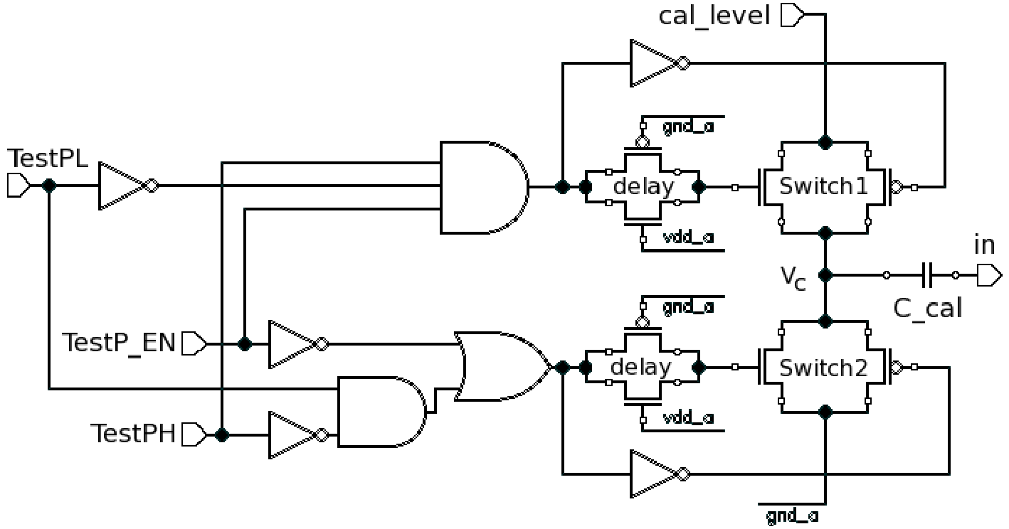
ToPix Version 3 Test Results
The ToPix v3 prototype has been tested on a bench to verify the performances.
The experimental setup foresees the testing board housing ToPix v3 and a Xilinx evaluation
board equipped with the Virtex 6 FPGA. The acquisition system is based on the LabView software.
Due to a problem in the column buses only the 32-cells column can work
at 160 MHz; therefore all the tests have been performed at 50 MHz.
The problem has been investigated and is partially due to the folded structure
of the column, which makes the bus significantly longer (by a factor of 1.3),
and partially from the fact that the 3 latches of each bit (due to the triple
redundancy) are directly connected to the bus without any buffer, thus
tripling the capacitive load.
Figure 3.43 shows the preamplifier output for differet input charge values
obtained with a threshold scan and the internal test signal generator. The obtained
shapes show the fast rising edge of the charge amplifier and the slow discharge at constant
current, even in the saturation case.
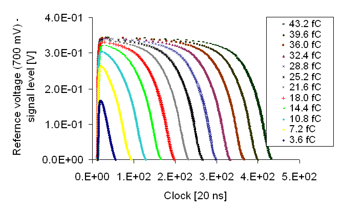
At present four ToPix chips have been tested, showing similar performances. Figure 3.46 shows the pixel response of the four tested samples. In the first row the chips which respond correctly to a sequence of 4 test pulses are shown in green. Pixels transmitting twice the correct number are marked in white, while pixels which do not respond at all are in black. Intermediate numbers of responses are shown accordingly with the colour scale. In the second and third rows, the leading and trailing edge values are represented, respectively. The time stamp values are represented in a colour scale. All the test signals are sent at the same time and with the same charge, therefore a uniform colour pattern is expected. Here pixels in black and in white correspond to a all 0’s and all 1’s output pattern, respectively. It can be seen that the number of defective pixels is slightly higher, apart from chip 2 where a column shows significant problems. It can also be observed that the variation of the trailing edge value is higher than the leading edge. This variation is expected due to the higher variation in the charge injection system and to the higher noise of the trailing edge.
Figure 3.44 shows the baseline level for all 640 pixels of a chip, before and after baseline equalisation.
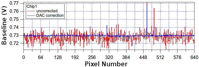
Figures 3.45 shows the baseline distribution before (left) and after (right) correction. A baseline sigma of 5 mV has been measured before correction, which correspond to an equivalent charge dispersion of 473 e-. After the correction with the on-pixel 5 bit DACs a dispersion of 650 V, corresponding to less than 62 e-, can be obtained. The measurements confirm the effectiveness of the correction DAC to reduce the threshold dispersion.
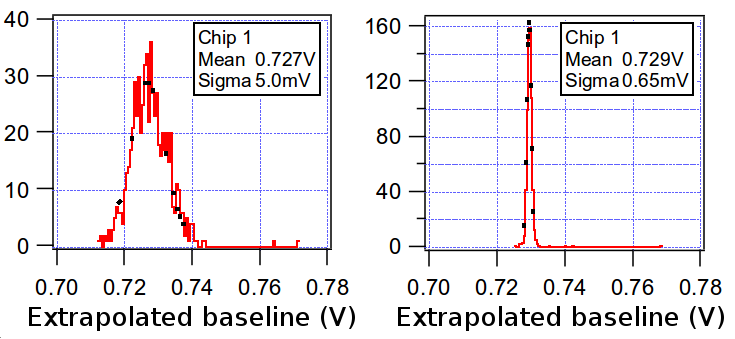
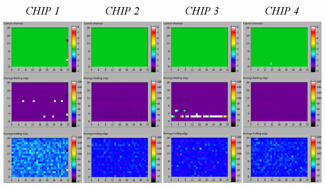
Figure 3.47 shows the measured gain. The measured value of 66 mV/fC is slightly lower than the simulated one (75 mV/fC) but compatible with the process variations and with the uncertainties of the charge injection mechanism.
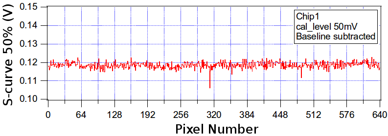
Figure 3.48 shows the measured noise. The average value of 100 e- obtained without the detector connected to the preamplifier input is consistent with a simulated value of 150 e- with the detector capacitance included.
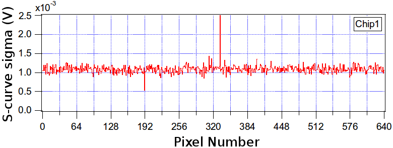
The charge to time overall transfer function is shown in figure 3.49 for the full charge input range and in figure 3.50 for charges up to 6 fC. Also shown in figure 3.49 is the deviation from the linear fit.
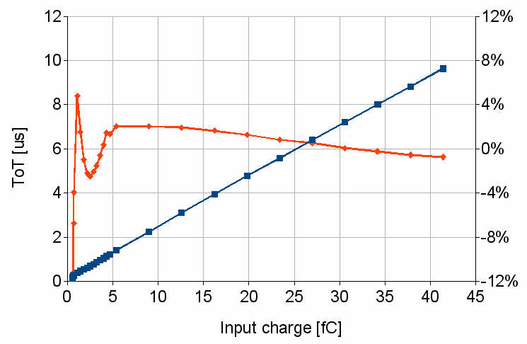
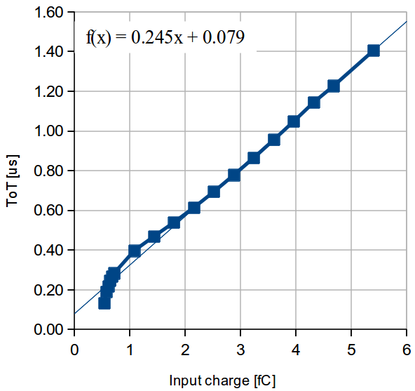
Due to the reduced clock frequency, the chip transfer function has been measured also for a feedback current which is half of the nominal value, in order to partially compensate for the reduction in charge resolution. The results are shown in figure 3.51 for the full range and in figure 3.52 for the first part of the dynamic range.
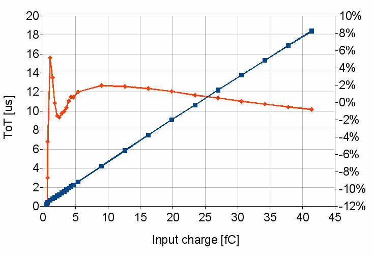
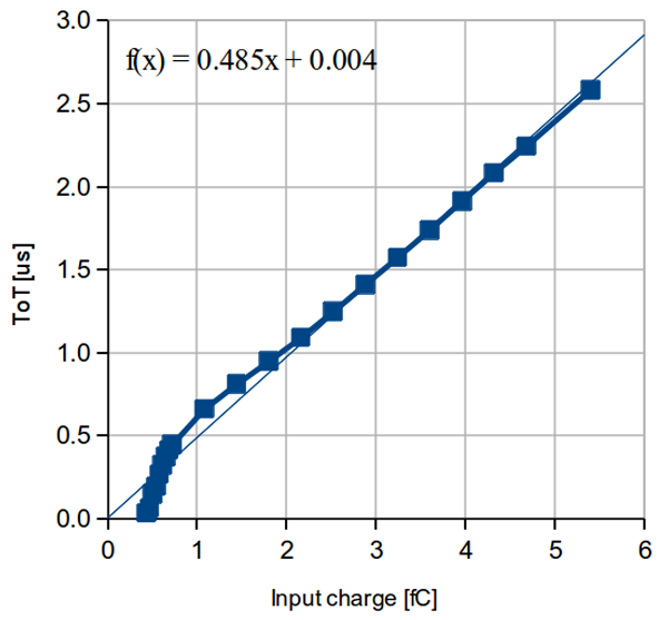
3.4 Hybridisation
Both the electrical and mechanical connections between the sensor and the readout chip are made by solder balls in a flip–chip solder–bonding process. This technique is now well developed for the application in the \PANDAexperiment not only for the daily connection process established in the FPGA production but also for the strong experience acquired in the LHC experiment realisation compared to the first solder flip–chip process developed by IBM in 1969 [ibm01].
3.4.1 Bump Bonding
Many companies (IZM, VTT, SELEX) have the capacity to perform the bump bonding process. Solder balls made of Sn–Pb or In have been used with good results in the LHC experiments. Balls sizes up to 20 m have been deposited on pads corresponding on one side to the pixel sensor and on the other size to the single readout cell. This technique can be regarded as well known. Pads on new epitaxial material and circuits made by the new 130 nm CMOS technology have been checked. The test of the first one is reported in the following subsection and test of the second one has been performed in an other experiment [Na62].
First Thinned Prototypes
With the first thinned prototypes described at the beginning of Section 3.2, the quality of the bump-bonding process was measured using a 90Sr source in self-triggered mode. Figure 3.53 shows the number of dead pixels for the tested assemblies (8192 pixels per assembly) [epi02]. In this case the term “dead” is used to cover several possible reasons for a pixel not being usable for signal acquisition, electronics channels with zero-gain, high channel noise due to high individual pixel leakage current, and failed bump connection. Apart from the S6 assembly which had an obvious localised problem covering a region of pixels, the connection yield and overall efficiency is very high, better than 99. An example of the source profile for the S8 (Epi-75) assembly is shown in figure 3.54 .
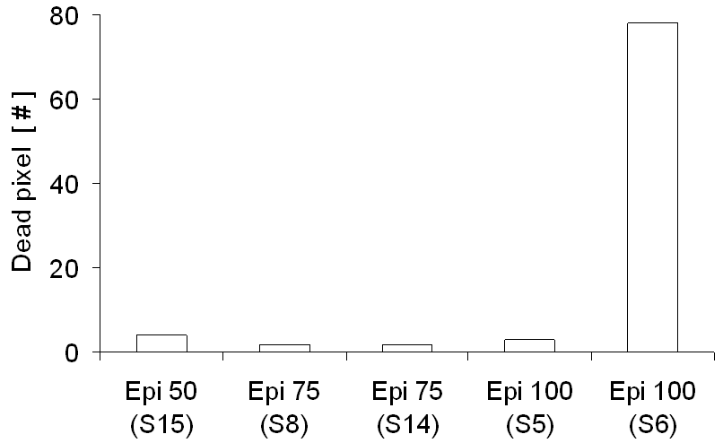
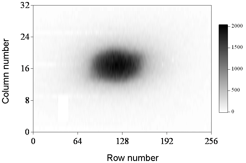
During the realisation of the first thinned sensor, unfortunately, all the epi wafers broke in the final stages of the thinning process, either during cleaning or during removal from the protective tape used to hold the wafers during thinning. One possible explanation is stress caused by significant differences in the lattice constants of the high-purity epitaxial layer and the heavily doped substrate. Then development work in collaboration with the VTT company was concentrated on understanding this problem better with the aim of resolving it.
In particular, a set of 12 patterned wafers, featuring 50, 75 and 100 m epitaxial thickness, with deposited bumps were thinned on the Cz side up to the target thickness of 200 m. This final thickness was selected with the aim to evaluate a possible contribution to the wafer breakage by the last passivation processes on the top of the patterned wafer, optimised for 200 m thickness as in the ALICE application.Only two wafers were destroyed during the thinning process, giving a yield of 83%.
Then 9 blank wafers with 100 m epitaxial layer were thinned in groups of three to the final thicknesses of 130, 120 and 110 m by removing most of the Cz substrate. The first two wafers broke during the CMP process used to remove the defect layers immediately after the backgrinding. The etching technique was planned at this time and no other breakage was detected with this last technique.
3.5 Single Chip Assembly Prototype
The first prototype of single chip assembly made of an ASIC developed in 130 nm CMOS technology, ToPix v3, and thinned epitaxial silicon sensor will be produced as the final step of the R&D phase for the hybrid pixel detector development.
The assembly is based on ToPix3, already described in the readout prototype section. The reduced scale of the pixel sensor matrix asks for a dedicated sensor layout. Figure 3.55 shows the pixel matrix layout made of 640 pixels to overlap the readout cell matrix of ToPix v3. On the perimeter the guard ring sequence, the first one connected to ground and the others in a floating configuration, is visible.
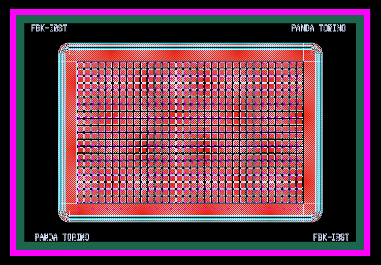
A second layout has been foreseen taking into account the larger pixels needed across the sensor region where two readout chips will be arranged side by side in the final project. This last prototype is made of 600 pixels and 40 pixels.
Figure 3.56 shows the schematic assembly between ToPix v3 and the sensor.
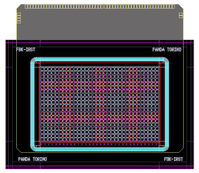
The pixel sensors have been arranged in 4 inch epitaxial wafers and produced at FBK. In particular MR and LR wafers as described in the Radiation Damage section have been used. Besides a wafer of each type was oxygen enriched. Figure 3.57 shows a sensor view by means of a microscope.
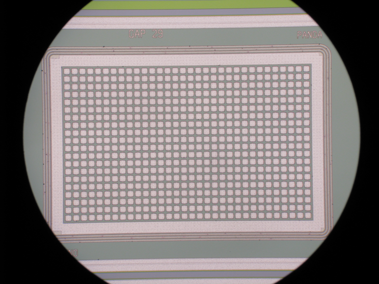
3.6 Module
The philosophy behind the design process of the pixel modules is to first optimise forward coverage, then adjust barrel design as a result. Only one variable is to take into account to perform this study, the chip size. Nevertheless a small production of silicon sensors as foreseen must fit on 4 inch wafers.
A hybrid pixel module is composed of several readout chips bump bonded to a unique silicon sensor, on the top of the sensor a multilayer bus routing both power supply lines and signal lines is foreseen equipped with minimal SMD components. Bus and readout chips are connected by wire bonding technique. Potentially a chip controller of this module could be arranged on the top of the bus to drive Gbit links and serving two or three readout chips.
Starting from the disks, the most useful sensor layout appears to be an alternating front and back configuration with respect to the carbon foam layer used to increase the heat transport to the cooling pipes embedded in the middle of this layer and acting as a mechanical support, too. In particular, a pixel active area of per chip is foreseen and 2, 4, 5, 6 readout chips sensors (S2, S4, S5, S6 respectively) are planned, with vertical gaps bridged with longer pixels as already explained in 3.2. The nominal readout chip size is or slightly less to include dicing tolerances. Figure 3.58 shows an S2 module scheme.
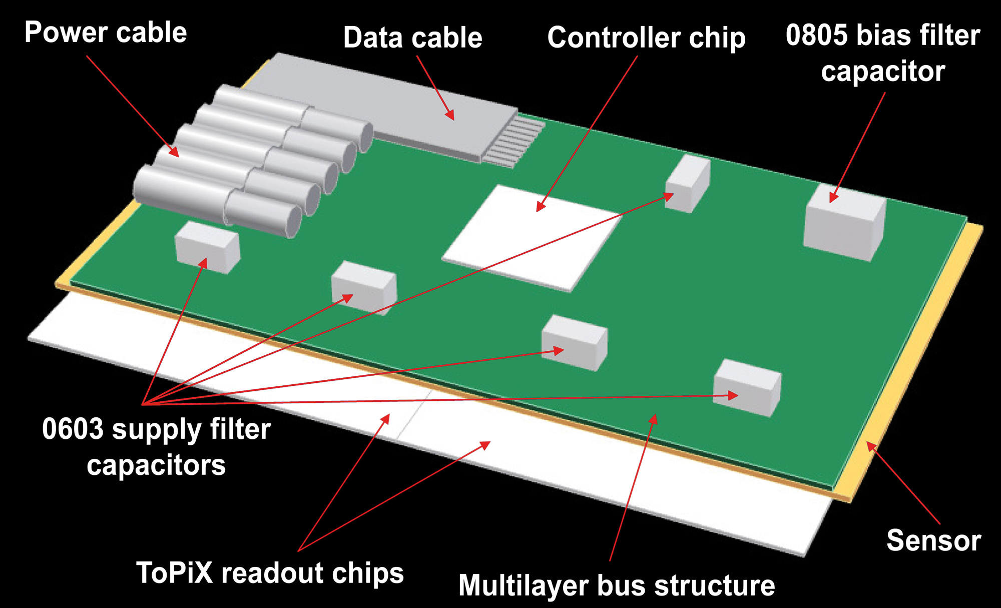
The small disks are equipped with six S2 modules and two S4 modules, with horizontal gap, and as starting point a sensor overlap due to the dead space driven by the conventional guard ring design. A geometrical total coverage of 65% is reached, but a systematic small shift will be studied to investigate the spatial distribution of the emitted particle tracks, to maximise the reconstructed hits. Figure 3.59 shows the module configuration of a small disk.
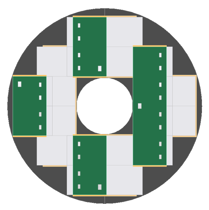
The big disks will be equipped with four S2, four S4, twelve S5 and four S6 modules. In this case a small dead zone (of about 1 mm) will result where two sensors meet in the horizontal plane. Figure 3.60 shows the module configuration of a big disk.
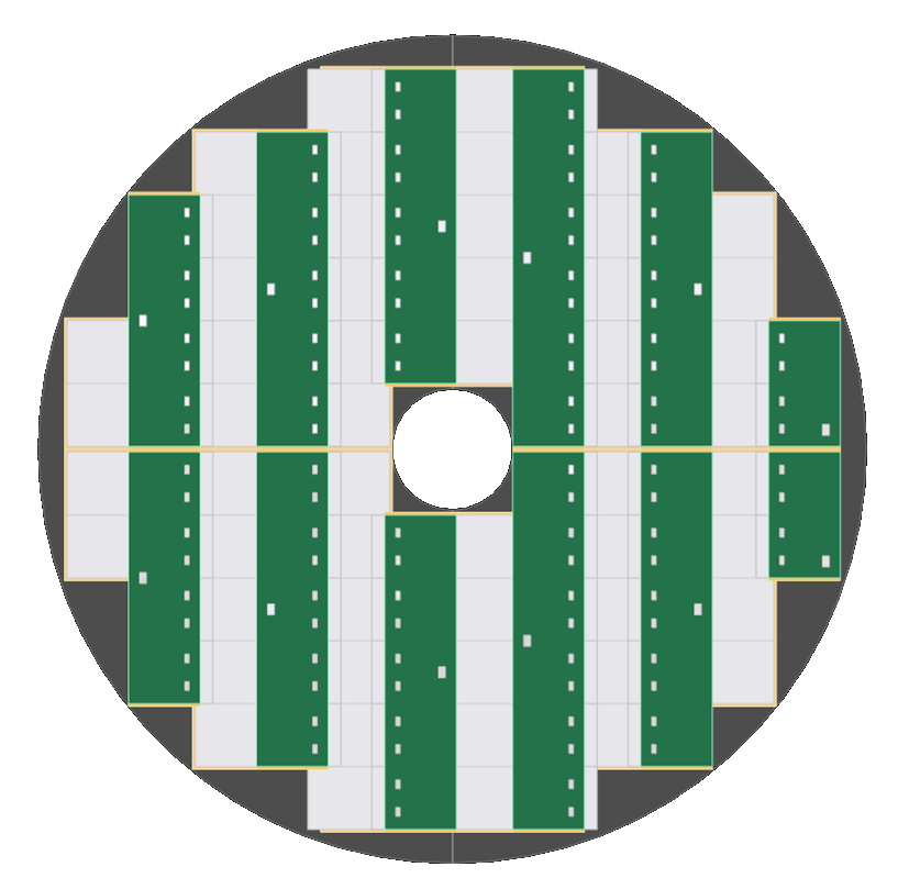
In general, keeping cables out of the active region will mean that some modules may require two designs according to which end the cables have to be connected.
In figure 3.61 the complete forward assembly is shown.
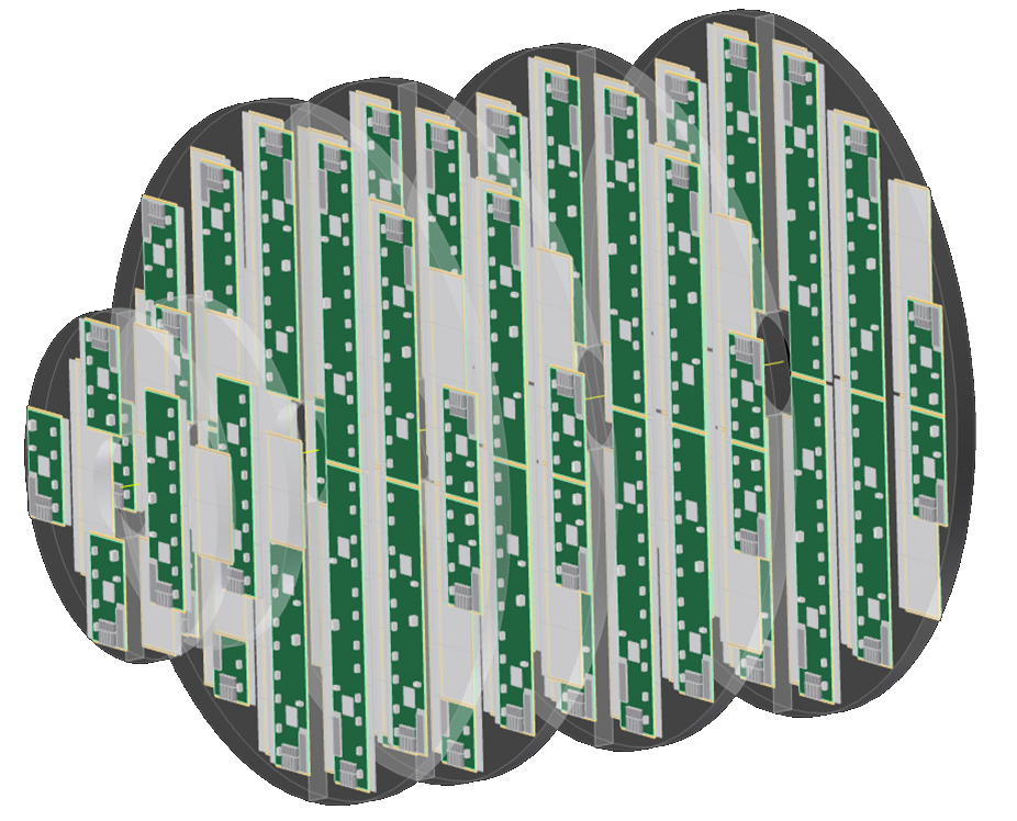
The pixel barrels are made of two layers of staves with modules featuring differently sized sensors to leave out the target pipe. The first layer houses 8 staves made of S4 modules and six staves based on S2 module each. The second layer is assembled from six staves made of S5 modules each and 22 staves housing two S6 modules each.
3.7 Bus-Flex Hybrid
The bus on the top of the sensor in a hybrid pixel module routes electrical signals and power lines. For minimising material and for handling high data transmission, different approaches, in particular for the electrical signals, have been followed studying this part of the project taking into account the two different solutions with and without a module controller serving two or three readout chips.
A first approach is based on a custom solution where at least two aluminium metal layers are interconnected with vias. The major parameters are: aluminium layer thickness of about 5 m, a minimum track pitch 100 m, a minimum via diameter 25 m, lowest possible dielectric constant to minimise thickness with the impedance control, the top layer compatible with wire bonding and SMD mounting, at least the overall structure size has to be compatible with a 4” Si wafer.
In figure 3.62 different size buses useful for different pixel modules are arranged inside an area suitable for a 4” Si wafer.
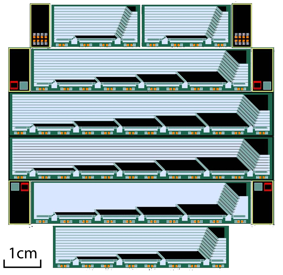
The bus layouts are designed for the case the module controller is not foreseen and a high density of tracks has to be handled and routed on the bus first layer up to a aluminium strip cable (see the Cable section in the Infrastructure chapter, 5.4). The second layer avoids the track crossing, e.g. of the clock line in case a single line is used for the whole module.
The feasibility of such a solution was investigated with a first company (Techfab, Italy). The base idea was to build the bus structures on silicon wafer as support and then take advantage of the Si–detector processes and quality lithography. SU–8 was identified as the most interesting dielectric for its relative dielectric constant (about 3). This lower value allows a dielectric thickness of about 15 m between Al layers. The electroless copper deposition was proposed as an useful process for filling the vias (figure 3.63).

Techfab went out of business after the very first process tests so that the project will now be pursued in cooperation with FBK, Trento. First test of SU–8 3010 was performed by using a strip-shaped mask. A layer that was only 19.6 m thin has been obtained as shown in the photograph of figure 3.64, where the wall of the strip shows a reverse angle (figure 3.65) not perfectly suited for aluminium deposition.
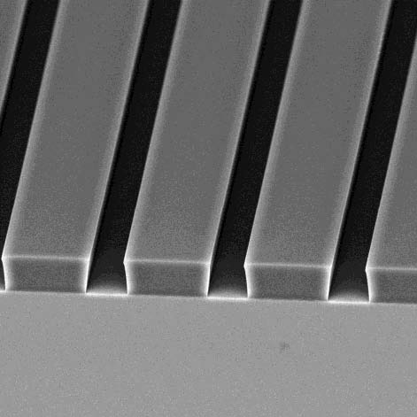
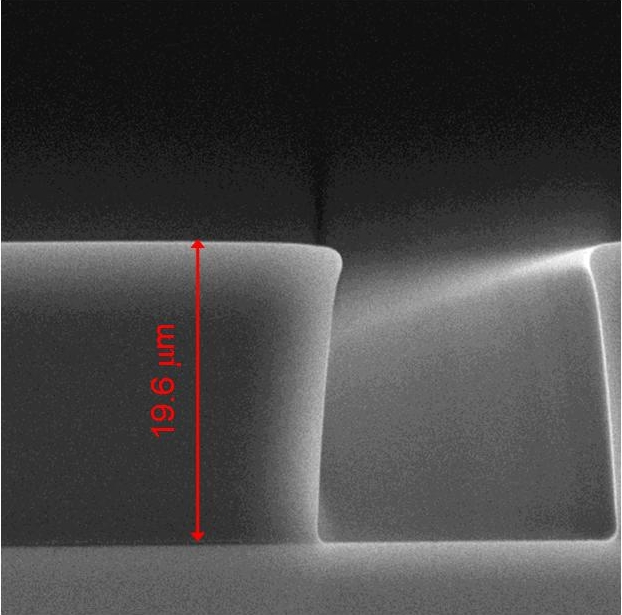
Besides an electroless technique with nickel appears to be better suited for the cleanliness of the manufacturing equipments.
In parallel to this new approach, a base solution has been considered using techniques developed at CERN for the Alice experiment. In this case a multilayer bus with a staircase shape (figure 3.66) houses deposited aluminium tracks featuring 80–90 m width and 150 m pitch on each layer and microvias between two layers have been made.
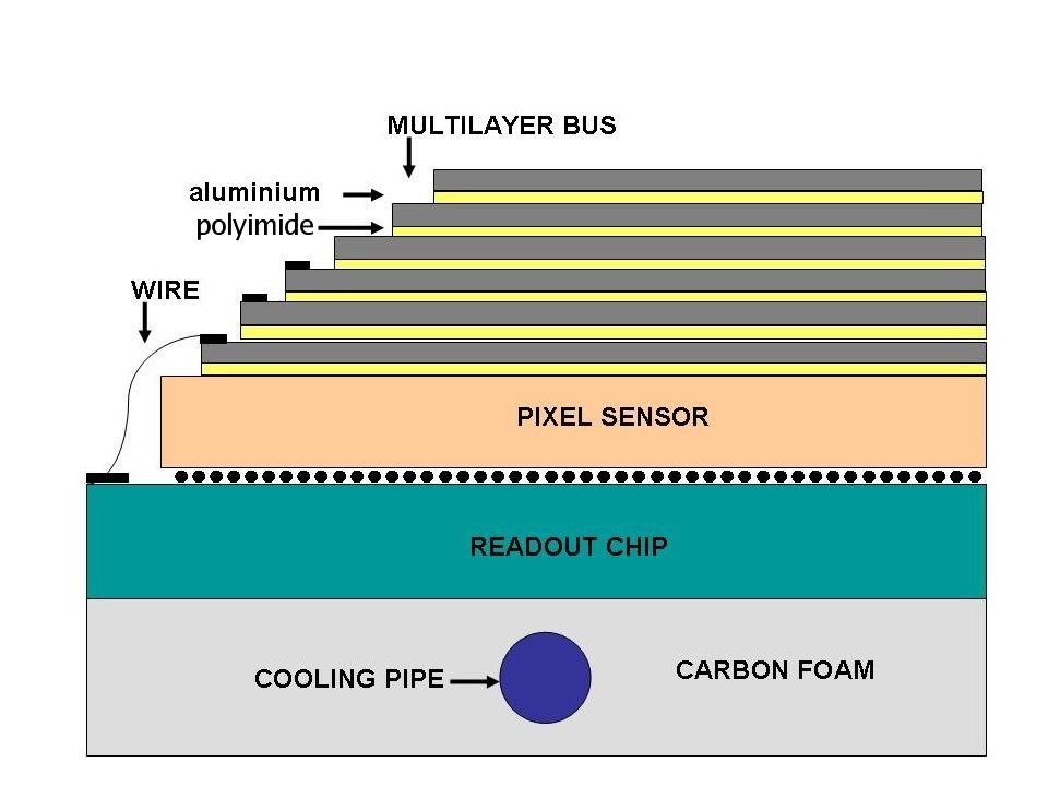
Alternatively to 10 m aluminium deposition, 15 m aluminium foil glued to polyimide has been considered. Different etching processes have been studied for both solutions [bus03].
As an example, in figure 3.67 a layout of a bus, foreseeing a module controller for the readout chips, is shown.

The power supply routing bus can be made of aluminium strips glued to polyimide, using the same technique that will be explained in the Infrastructure chapter, Cable section (5.4) for data transmission. Analogue and digital power supply lines planned for the readout chips and the bias voltage for the sensor with corresponding ground planes will be the first layers of the staircase bus on the top of the sensor.
References
Chapter 4 Silicon Strip Part
This chapter describes the silicon strip part of the MVD, which consists of a barrel and a forward disk section as outlined in section 2.4. The basic design foresees double-sided strip detectors of rectangular and trapezoidal shape, respectively. The overall concept of the MVD is based on a standard process for radiation hard sensors with a target thickness of 200 to 300 m. It follows approved solutions of other tracking systems already installed at HEP facilities. As for the entire apparatus the trigger-less readout concept represents one of the major technical challenges and requires the implementation of new technologies. Moreover, the readout on both sensor sides requires sophisticated technical solutions for the hybridisation of the detector modules.
4.1 Double-Sided Silicon Strip Detectors (DSSD)
Presently silicon strip detectors are deployed to a great extent as tracking detectors in particle physics experiment worldwide. The division of the semiconducting detector by means of strips enables a one-dimensional spatial resolution of particle tracks traversing the detector. The utilisation of double-sided strip detectors offers the ability of precise point reconstruction with the advantage of less detector channels compared to pixel detectors. However, ambiguities occur in case of multiple particles crossing the detector in the same time frame. Therefore the \pandaMVD utilises silicon strip detectors at the outer layers of the MVD where the particle flux is reduced in contrast to the inner layers.
4.1.1 Barrel Sensors
First \pandafull size prototype sensors have been produced in the first half of 2011 by the company CiS GmbH in Erfurt (Germany). The production process utilises a 10+2-layer process with a single metal layer laid out on 4′′-wafers consisting of ⟨111⟩ - cut material. A floorplan of the designed layout of the implemented structures can be seen in figure 4.1.
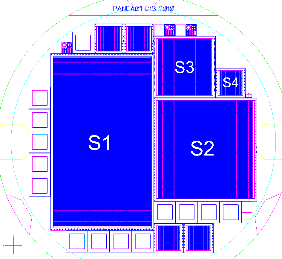
Table 4.1 gives an overview of the specifications of the wafer and of the implemented sensors. As starting material, a monocrystalline Floating Zone (FZ) silicon wafer was chosen. For the implemented sensor structures front side strips are realised as p+ in n doping, whereas the back side contains n+-strips embedded in the n-substrate. All sensors are double-sided with strip structures oriented orthogonal to each other on either side. The depletion is achieved by punch-through biassing from the bias ring towards the strips on both front and back side and the n-side charge separation is realised by p-spray implants. The active area is protected by eight guard rings to assure a stable electric field within the active area. In this scheme, front side is considered the junction contact, or p-side, while the ohmic, or n-side, is always referred to as back side.
| General | |
|---|---|
| wafer material | FZ Si, 4′′, n/P |
| thickness | 285 10 m |
| resistivity | 2.3 5.0 k |
| n-side isolation | p-spray |
| guard rings | 8 |
| stereo angle | 90° |
| passive rim | 860 m |
| S1 | |
| n-side strips | 896 |
| p-side strips | 512 |
| pitch | 65 m |
| active area | 58.275 33.315 mm2 |
| S2 | |
| n-side strips | 512 |
| p-side strips | 512 |
| pitch | 65 m |
| active area | 33.315 33.315 mm2 |
| S3 | |
| n-side strips | 384 |
| p-side strips | 384 |
| pitch | 50 m |
| active area | 19.230 19.230 mm2 |
| S4 | |
| n-side strips | 128 |
| p-side strips | 128 |
| pitch | 65 m |
| active area | 8.355 8.355 mm2 |
Besides the full size \pandaprototype sensors, a smaller, square shaped sensor S3 with 50 m pitch and an active area of roughly 2 2 cm2 was realised on the delivered wafer (see figure 4.2). This sensor was foreseen to be an equally sized replacement for already existing prototype sensors from earlier prototyping stages in order to benefit from the existing readout infrastructure. Furthermore, five “Baby”-Sensors (S4) with only 128 strips on either side were placed on the wafer. Additional test structures are implemented as well, serving mainly as markings during wet-processing stages, bonding calibration tags or similar. Finally, fourteen diodes with different numbers of guard rings are placed around the main elements on the wafer. These diodes may be used to derive the radiation dose during irradiation tests.
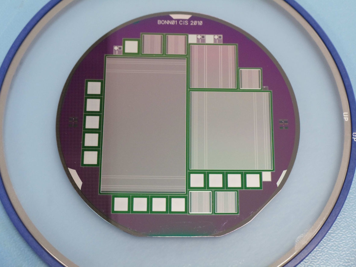
In figure 4.3 a corner of the sensors on the n-side (left picture) and one on the p-side (right picture) are shown with the first strips and the high potential bias contact ring with square-shaped passivation openings. The pads on the n-side strips are connected to the odd-numbered n+-implants, while the even-numbered pads are located at the opposite edge (not shown). On the junction- or p-side additional guard ring structures for insulation of the high potential difference to the bias line are necessary. The contacts along the inner bias line are used for the supply of the negative bias potential. The DC-pads on the strips are direct connections to the p-side p+-implants. For ease of channel identification, additional orientation numberings and position marks are implanted inside the metal layer.

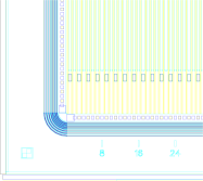
A measurement of the leakage current flowing through the sensor with applied variable reverse voltage at the bias contacts is shown in figure 4.4. The recorded curves are the I-V - characteristics of the large sensors (6.0 3.5 cm2) from 25 different wafers out of two lots. Almost all of the sensors show the expected behaviour, i.e. very low and constant leakage current above full depletion and a steeply increasing current at reverse breakdown voltage. Two of the analysed sensors obviously completely fall off this pattern; one which shows a continuous strong rise of the current even at low voltages and one that appears to become depleted at all but shows excessive leakage at higher voltages. It is already clear from this first picture that sensors past production should be casted into quality categories to ensure equal parameters of the sensors utilised in a collective context (in this case the modules inside the MVD).
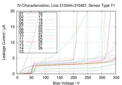
The full depletion voltage for each sensor is extracted before the actual assembly takes place. This is done in a probe station setup by sampling the capacitance vs. bias voltage characteristics as seen in figure 4.5. The p-side single strip capacitances are measured with typical values of 450 fF at a depletion voltage of 150 V. For comparison the total capacitance at the bias contacts (black trace) is shown. In order to assure error-free operation inside the \panda-detector a procedure is suggested that allows the selection of sensors whose parameters satisfy following criteria:
-
•
the global leakage current must not exceed 10 A below breakdown voltage
-
•
the global capacitance must show clear depletion above full depletion voltage
-
•
the breakdown voltage must be at least 50 V higher than the maximum foreseen bias voltage of 200 V
In the first 2011 prototyping batch 80% of the delivered sensors (type S1) conformed to these criteria. It is expected that the yield increases once the production parameters are fixed and the producing site imposes post production tests allowing the delivery of sensors according to these criteria [hgz-long-communication].
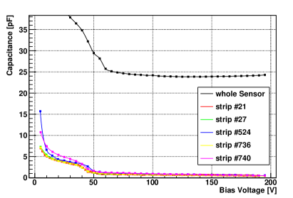
For the qualification of radiation hardness the S4 sensors (128 strips on either side with a pitch of 65 m) have been irradiated with protons and neutrons of several fluences in order to categorise the obtained sensors with respect to the systematic radiation damage studies undertaken by the RD48 collaboration [rd48-report]. Particularly the definition of the maximum depletion voltage of 200 V necessary to operate irradiated sensors at the end of the full \pandalifetime with an applied fluence of \neueqis derived from these collected data (see figure 4.6). With this choice an additional oxygen enrichment stage is not mandatory but left as optional degree of freedom to compensate for possible yield losses.
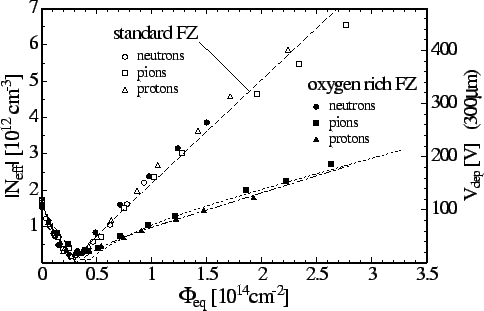
Irradiations with slow (14 \mev) protons were carried out at the cyclotron facility in Bonn with a total fluence of up to pcm which corresponds to a 1 \mevneutron equivalent fluence of roughly cm obtained by NIEL scaling. I-V and C-V - characteristics of the irradiated sensors (type S4) have been measured in different time intervals after the end of the irradiation (figures 4.7 and 4.8). The measurements took place between annealing intervals of 20 hours (red curves), 310 hours (green curves) and after an annealing at a temperature of 60 ∘C for 24 hours (blue curves). The green curves correspond to the standard annealing interval of 80 min in a 60 ∘C environment as proposed by [rd48-report]. The I-V - trends in figure 4.7 are normalised to the volume leakage current in order to have a proper comparison to measurements available from other groups. The obtained leakage current of 1 after irradiation meets well with the value to be expected from field studies [Moll-paper].
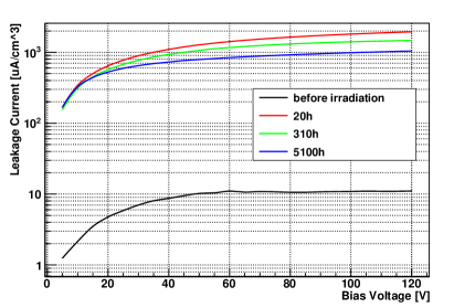
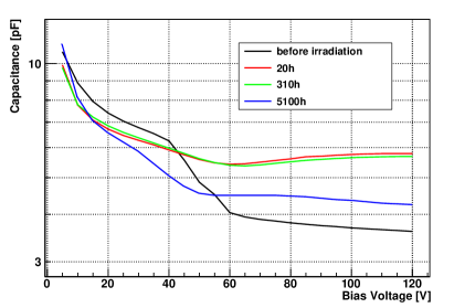
The recorded post-irradiation C-V - trends in figure 4.8 show nicely the expected beneficial (red and green) and reverse (blue) annealing behaviour as well as the change in the full depletion voltage from 60 V to 50 V due to the change in the doping concentration according to figure 4.6 and thus demonstrate the suitability of the first batch of prototype sensors for the targeted requirements.
4.1.2 Wedge Sensors
Basically, the technological option chosen for the wedge sensors will be the same than for the barrel sensors. A picture of the main sensor layout is shown in figure 4.9.
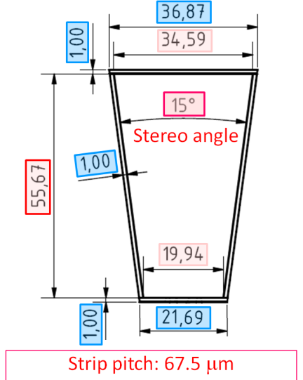
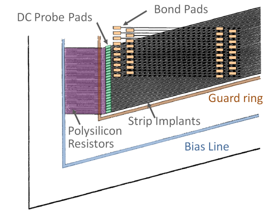
The active area of 1517 mm2 stays below the one for the rectangular barrel sensor (1941 mm2) so that major characteristics of the sensors are expected to be in the same range than the ones of the already tested full size barrel prototypes. In contrast to the barrel sensor, the readout pads on both sides will be at the same sensor edge. Strips run parallel to one of the edges of the trapezoid. Thus, those on the opposite side get shorter when approaching the sensor edge. A connection scheme adapted from [D0-WedgeLayout] is shown in figure 4.10. Basic design parameters of the sensor are listed in table 4.2.
| Strip pitch | 67.5 m |
|---|---|
| Strip orientation | to sensor edge |
| Number of strips | 512 / side |
| Stereo angle | 15∘ |
| Sensor height | 57.67 mm |
| Total area | 1688 mm2 |
| (Active area) | (89.9%) |
4.2 Front-End Electronics ASIC
4.2.1 Requirements
The data acquisition concept of the \pandadetector demands \frontendelectronics that is able to run without the need of an external trigger. Therefore the \frontendmust be able to distinguish detector noise from physical events and send this hit information together with a precise time stamp to the data acquisition.
A decision towards the \frontendto be deployed for the strip part of the \pandaMVD has not yet been made. The \frontendshould feature a measurement of the deposited charge of a particle crossing the detector in order to achieve a spatial resolution through clustering algorithms. This energy loss measurement may also be used for a particle identification hypothesis (PID). Since only digital information about the charge measurement should be transfered from module level, the digitisation should be done on the front-end. Digitisation can be achieved via the Time-over-Threshold method (ToT) or sampling-ADCs. Regardless whether ToT or ADCs will be utilised a low power consumption should be aspired. The digitisation resolution should be in the order of 8 bit or better to ensure a precise charge measurement and, moreover, a high spatial resolution. Assuming linearity of the digitiser within a dynamical range of 10 minimum ionising particles, 8 bit are required to assure that the least significant bit will be comparable with the one sigma detector noise. In order to save board space and number of data cables the \frontendshould feature highspeed serial data links. The \frontendshall be radiation hard to a level of up to 10 MRad. The time-stamping of observed hits will be done with the \pandatiming clock of 155 MHz. Table 4.3 summarises the requirements for the strip readout \frontend.
| Parameter | Value | Remarks |
| Geometry | ||
| width | 8 mm | |
| depth | 8 mm | |
| input pad pitch | 50 m | |
| pad configuration | lateral pads occupied only for diagnostic functions, should be left unconnected for final setup | |
| channels per \frontend | default: 128 channels | |
| Input Compliance | ||
| sensor capacitances, | ||
| fully depleted sensor | ||
| 10 pF | rect. short strips | |
| 50 pF | rect. long strips + ganging | |
| 20 pF | trapezoidal sensor | |
| input polarity | either | selectable via slow control |
| input ENC | 800 e- | = 10 pF |
| 1,000 e- | = 25 pF | |
| Signal | ||
| dynamic range | 240 ke- ( 38.5 fC) | |
| min. SNR for MIPS | 12 | 22,500 e- for MIPs in 300 m silicon, guaranteed within lifetime |
| peaking time | ns | typical Si drift times |
| digitisation resolution | 8 bit | |
| Power | ||
| overall power dissipation | 1 W | assuming 128 channels per \frontend |
| Dynamical | ||
| trigger | internally generated | when charge pulse exceeds adjustable threshold value |
| time stamp resolution | 20 ns | |
| dead time / ch | 6 s | baseline restored to 1% |
| overshoot recovery time / ch | 25 s | |
| average hit rates / ch | derived from simulations at | |
| (poissonian mean) | a beam momentum of 15 \gevc | |
| hot spots | 9,000 s-1 | \pbarp |
| 40,000 s-1 | \pbarAu | |
| average occupancy | 6,000 s-1 | \pbarp |
| 30,000 s-1 | \pbarAu | |
| Interface | ||
| slow control | any | low pincount, e.g. I2C |
| data | sparsified data | |
4.2.2 Options
Currently there are no \frontendASICs available to fully comply with the demanded requirements. However, there are developments for self-triggering \frontendswhich are mostly in an early prototyping state. The available and future developments will have to be tested with respect to the demands of the MVD. Some of the \frontendoptions are presented below.
Modified ToPix Version 3
The use of very similar \frontendarchitectures for both pixel and strip sensors in the MVD opens interesting perspectives. In this case, in fact, the back-end electronics for the two sub-systems could share the same hardware design, with minimal customisation being done at the firmware and software level. Such an approach would allow important synergies inside the MVD community, reducing the development time and costs of the overall project. However, the two sub-detectors differ significantly in key specifications, such as the sensor capacitance (few hundreds of femtofarad for the pixels and several picofarad for the strips), data rate (few kilohertz per pixel versus about ten kilohertz per strip) and power consumption per channel (few microwatts in case of pixels and few milliwatts for the strips). From these numbers, it is apparent that the two parts of the MVD demand a detailed customisation of the very \frontendelectronics.
In ToPix, the \frontendASIC for the pixel sensors described in chapter 3.3.3, the Time over Threshold technique (ToT) has been adopted to digitise the charge information. In this approach the feed-back capacitor of a high gain amplifier is discharged with a constant current. The time during which the amplifier’s output remains above a given threshold is measured by counting the clock pulses. One of the interesting features of the method is that the linear dynamic range is extended well beyond the saturation point of the amplifier. This combines low power operation with the capability of measuring energy losses much greater than those ones of minimum ionising particles.
In the present design, the input amplifier employs a single stage topology. This choice was dictated by the limited space available in the pixel cell for the implementation of the analogue part (50 m 100 m). One of the drawbacks of this configuration is the increased sensitivity to cross-talk for large input signals that saturate the amplifier. When this happens, the amplifier’s open-loop gain drops, thereby determining an enhancement of the cross-talk between adjacent channels through the inter-electrode capacitance. For pixel sensors this capacitance is small and such an effect can be tolerated. However, the saturation of the input stage would be a serious issue for strip sensors, where the inter-strip capacitance may reach several picofarads.
The measure of the charge with the ToT gives a variable dead-time. The high granularity of the pixels (cell size of 100 m 100 m) reduces the event rate per channel to the kHz level and dead times of several microseconds can hence be tolerated. For strip sensors, on the other hand, the event rate per channel is significantly higher.

Figure 4.11 shows a possible adaption of the ToPix architecture that would take into account the aforementioned issues. The input stage is a charge sensitive amplifier followed by a pole-zero cancellation network. This block can be seen as a current amplifier with Gain . By properly sizing and one can limit the signal swing at the preamplifier output, so the saturation is avoided. In this way, an adequate loop gain is always maintained and the cross-talk is minimised. The input stage is followed by a current buffer, which provides additional gain and drives the ToT block with proper impedance. The ToT stage has the same topology of the pixel cell in ToPix. A constant current discharges the feed-back capacitance of an integrator. The start and stop time of the discharge are measured by latching into local registers Gray-encoded words provided by a counter which is common to all channels. Assuming the standard reference clock of \pandaof 155 MHz a 10 bit resolution translates into a maximum dead-time of 6.4 s. The average dead-time will be significantly smaller, since higher input charges which leads to longer signals are less probable. By using more ToT cells per channel a derandomisation of the arrival time is achieved. Assuming an average dead time of 6.4 s (which is very conservative for 10 bit resolution) and four digitising cells one can accommodate a rate of 100 kHz per channel with an efficiency better than 99.5%.
Preliminary simulations of the architecture were done using the parameters of the same CMOS process chosen for the prototypes of the pixel \frontendelectronics. The strip-optimised front-end shows a noise of 1000 electrons rms for a power consumption of 1 mW per channel. From the readout point of view each channel, which contains four independent digitising elements, can be seen a “short” pixel column with four pixels. Such similarities would of course favour the development of a common readout framework and the reuseability of different modules and concepts between the two subsystems.
STS-XYTER
The STS-XYTER is a development based on the n-XYTER [NXYTER-paper]. It will make use of the same token-ring-architecture common to the n-XYTER. It is supposed to be a dedicated \frontendASIC for the readout of silicon strip detectors to be used in several \Fairexperiments. The \frontendwill feature a self-triggering architecture and is designed for low power consumption. Therefore it will make use of a ToT-based digitisation. In order to handle the data rate in high occupancy environments a fast digital link with a data rate up to 2.5 Gbps is envisaged. Two prototype ASICs - TOT01 [STS-XYTER-Test1] and TOT02 [STS-XYTER-Test2] - were produced and tested. Further specifications and parameters measured with first prototypes can be extracted from table 4.4.
| Parameter | adapted ToPix | STS-XYTER | FSSR2 |
| input pad pitch | 50 m | 50 m | 50 m |
| channels per \frontend | 128 | 128 | 128 |
| dynamical range | 100 fC | 15 fC | 25 fC |
| ENC | 1,000 e- @ 20 pF | 700 e- @ 28 pF | 240 e- + 35 e-/pF |
| peaking time | 6 ns | 80 ns | 65 ns |
| power consumption | 0.8 mW/ch | 1.2 mW/ch | 4.0 mW/ch |
| trigger | self-triggering | self-triggering | self-triggering |
| digitisation technique | ToT | ToT | Flash-ADC |
| digitisation resolution | 10 bit | bit | 3 bit Flash-ADC |
| time resolution | 1.85 ns @ 155 MHz | 1.85 ns @ 155 MHz | 132 ns time stamp |
| data interface | e-link - SLVS | up to 2.5 Gbps | LVDS |
| number of data lines | 1 pair | 1 pair | 1 to 6 pairs |
| slow control | custom (serial) | custom | custom LVDS |
| process | 0.13 m CMOS | UMC 0.18 m | 0.25 m CMOS |
| radiation hardness | 10 MRad | 10 MRad | up to 20 MRad |
FSSR2
The FSSR2 [fssr-paper1] is a 128-channel ASIC for silicon strip readout. It features a fast, self-triggered readout architecture with no analogue storage, similar to the FPIX2 chip (the pixel \frontendfor the BTeV experiment) where it was derived from. Each analogue channel contains a programmable charge sensitivity preamplifier, a shaper with selectable shaping time, a selectable base line restorer and a discriminator. The discriminator with an adjustable threshold simply yields a binary hit information. Moreover each channel contains a 3-bit flash ADC with selectable thresholds to achieve an amplitude information.
4.3 Module Data Concentrator ASIC
4.3.1 Architecture
Each strip sensor module will have the \frontendchips as well as a module controller on board. The module controller serves as link between the \frontendchips and the MVD detector data acquisition-system. The module controller has to be able to handle sensor modules of different sizes up to the maximum of strips corresponding to the large double-sided sensors outlined in table 4.1. The main tasks to be performed are:
-
•
readout, decoding and multiplexing of \frontendchip data;
-
•
buffering, pedestal subtraction and optional one-dimensional or two dimensional clustering;
-
•
interfacing to DAQ via serial GBT [gbt] E-links;
-
•
slow control functions (parameter transfer, monitoring).
The module controller has to be finally realised as a fully digital ASIC in radiation-hard technology. Since just one module controller is needed for each sensor module, the additional material budget, the current consumption and the thermal load of this component will be neglegible compared to that of the \frontendchips. The design of the module controller is currently in progress [PANDA-KolMet]. To have a starting point, it is assumed to use the n-XYTER plus a separate ADC as \frontendhardware. In this case, 11 n-XYTERs and ADC’s are needed for the largest strip sensor module. The design is fully VHDL-based using Xilinx FPGA as technological platform. The modular structure of the design guarantees a minimum effort to incorporate different \frontendsolutions or additional features in future versions.
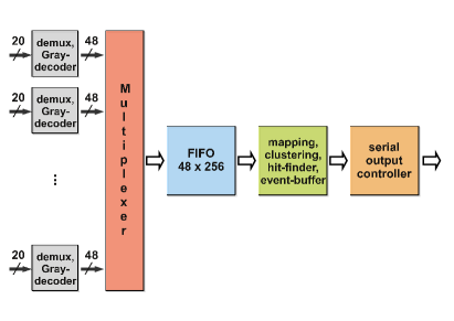
4.3.2 Implemented Feature Extraction Algorithms
The data frames from the different \frontendchips contain the time stamp, strip-identifier and charge information. After subtracting the pedestal from the charge the frames are stored in a FIFO, from which they may be extracted in the raw format or a feature extraction may be performed by the module controller. With the foreseen feature extraction stage enabled, the module controller will continuously scan the FIFO output and collect frames of a certain time interval . is determined by bit-truncation of a parameter-based number n of least significant bits from the time stamp. The corresponding frames are buffered and analysed for clusters with a minimal multiplicity m of next and next but one hits in the - and -strips of one sensor module [Koop]. If hits are detected, the time stamp, the centroid, the width in the - and -plane, the sum of charges and the multiplicity will be stored in the hit-register. The contents of the hit register may be transferred to the DAQ system or, if enabled, passed to a 2-dimensional correlation stage that generates a list of all possible x-y-combinations of clusters. For each possible combination a combinatorial and a charge-correlation probability is calculated based on the utilisation of fast look up tables, particularly of error functions. The resulting 2d-clusters then are buffered in the output FIFO. Important clustering parameters, like the minimal multiplicity m, the number n of truncated bits in the time stamps, the cluster thresholds or the cutoff threshold of the combinatorial probability are adjustable via the slow control interface.
4.3.3 Implementation Status
The VHDL-design is expected to be finished in 2011. First test were performed using device simulations. The design is able to buffer up to 5 simultaneous hits at the n-XYTER clock speed of 128 MHz. Based on a Xilinx Spartan 6-device timing simulations resulted in approximately 150 ns for the multiplexing of the 11 \frontenddevices (n-XYTER plus ADC). The current consumption and thermal load strongly depend on the technology chosen for the final ASIC design and have to be evaluated later. Since the final decision concerning the \frontendchip for the strip sensors has not been reached yet, the module controller design still has to be adapted to the final \frontendand transfered to the appropriate ASIC technology basis.
4.4 Hybridisation
4.4.1 Overview
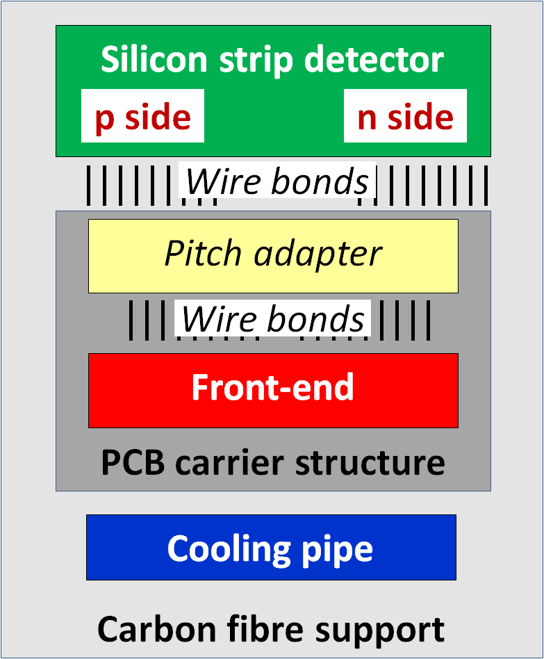
The hybridisation of double-sided strip detectors is one of the technically most demanding tasks for the strip part of the MVD. Particular challenges arise from the electrical connection on both sensor sides, as described in chapter 5.3.3. Figure 4.13 gives a schematic illustration of the overall concept. In contrast to the hybrid pixel design, readout electronics can be placed outside the acceptance of the sensors. Therefore, appropriate adapter components are introduced to interconnect to sensor and the \frontendelectronics. Wire bonding is the default option for all electrical connections from the sensor to the \frontendchip. Basically, the layout of the readout pads on the senor differs from the one on the \frontend. This accounts for both the effective contact area as well as the pitch, i.e. the interspacing of two neighbouring pads. Technical limitations of the wire-bonding process must be considered if the pitch size is smaller than 100 m as it is the case for the wedge sensors and the input channels of the \frontend. These require parallel straight-line connections between corresponding pads, which can be achieved by the introduction of a fan-like structure. Such pitch adapter can be either integrated on the hybrid carrier PCB or designed as an individual component. While the first option represents an advanced technical solution, the other one follows the solution of other HEP experiments recently installed. Finally, the detector module must be integrated onto a local support structure in order to achieve the required mechanical stability. The local support structure includes a cooling pipe needed to prevent a heating of the readout electronics or the sensors.
4.4.2 Basic Approach for the MVD
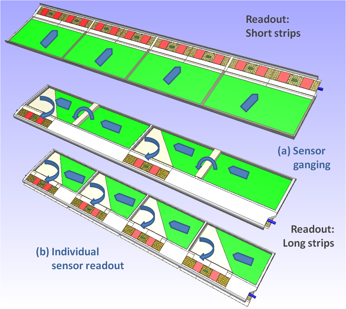
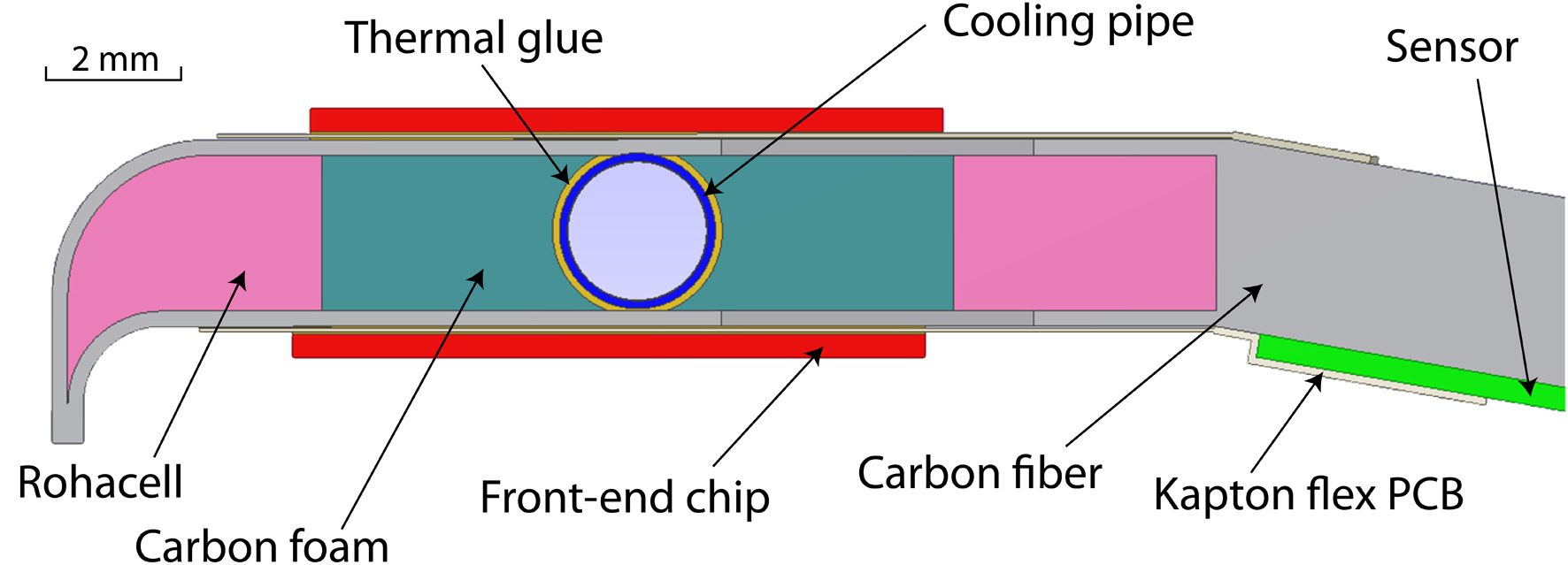
The different sensor geometry as well as the changed sensor orientation with respect to the beam pipe lead to individual hybridisation concepts in the barrel and the forward part. Figure 4.14 illustrates the basic approach for the strip modules in the barrel layers. A complete super-module contains several sensors, which are aligned in one row. The carbon fibre support structure is extended at the long edge thus leaving space for the positioning of the \frontendelectronics. Due to the stereo angle of 90∘ the sensor is read out at two edges. A flexible carrier structure is introduced to flip the \frontendsat the short side by 90∘ to the support frame. The overall number of readout channels can be further decreased by connecting strips of neighbouring sensors. However, this option is technically more challenging and may cause deteriorations of the overall performance. Therefore, a fall-back solution is given by an individual readout of all sensors. A schematic cross section through a hybridised strip module is shown in figure 4.15.
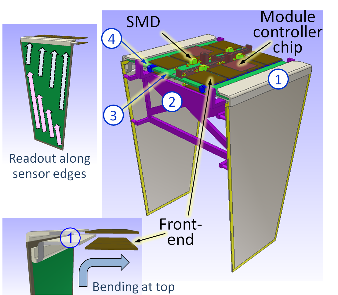
The hybridisation concept of the strip disk part follows the basic idea presented in [HermesLambdaWheels]. A disk super-module combines two successive sensors of the two layers. In contrast to the barrel sensors the readout of both sensor sides is performed at the same sensor edge at the top. Flexible adapter pieces facilitate a bending by 90∘ so that the \frontendelectronics can be placed at the top plane in the gap between the two sensors. In this way a minimum radial occupancy of the passive elements can be achieved. While a flat support serves as contact surface for the PCB carrier board, a more sophisticated carbon support structure is needed to combine the readout plane at the top and the two sensors to a compact and robust object. An illustration of the hybridisation concept for the strip disks is given in figure 4.16.
4.4.3 Layout of Hybrid Carrier PCB
The material of the \frontendelectronics carrier structure should satisfy the following requirements:
-
1.
low thickness at high structural integrity, low-Z compound;
-
2.
well defined dielectric constant up to frequencies of at least 1 GHz and; low dielectric loss at the same time;
-
3.
radiation tolerance, i.e. insignificant change of properties under irradiation in ionising as well as non-ionising fields.
From readily available materials only few fulfill all of these demands. An optimal choice seems to be Kapton111developed and patented by duPont-Polyimide (chemical composition: Poly-(4,4′-oxydiphenylene-pyromellitimide)) since beside the mentioned requirements additional advantages, e.g. easy bondability with metal-films and wet-processing with standard-PCB-structuring techniques are applicable [kapton-datasheet].
| material | kapton polyimide |
|---|---|
| dielectric thickness | 25.4 m |
| dielectric constant | 3.4 |
| dielectric loss tangent | 0.004 |
| conductor type | Cu |
| conductor thickness | 18 m |
| radiation length (min-max) | % |
For the hybrid carrier PCB a two layer layout is foreseen with the parameters given in table 4.5. The value for radiation length for this material is in general very low but may peak up to ca. 0.25% locally, when copper traces or larger areas on both sides overlap.
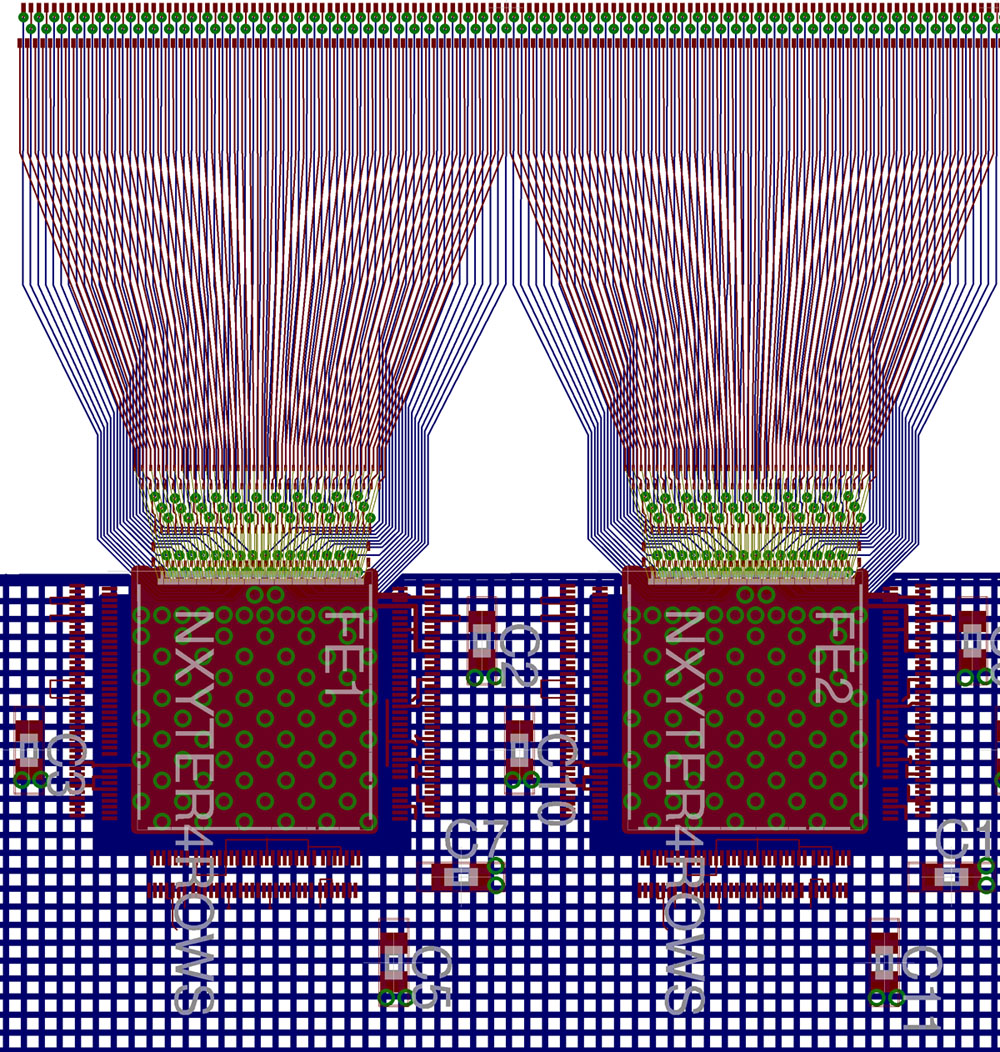
The fan-in routing of the default 130 m pitch structure to the \frontendpitch can be processed by standard PCB manufacturing techniques. Figure 4.17 shows a layout of a prototype for the connection to already existing n-XYTER \frontendASICs which is being produced and evaluated at the moment. The bonding pads at the top edge are placed in two staggered rows at the sensor pitch. The next step is the interconnection of this hybrid prototype to the sensor by directly glueing the PCB with an overlap of 6.7 mm onto the sensor such that the innermost AC-pads of the sensor and the bonding pads on the flex-PCB face each other and can be connected via bonding wires.
4.4.4 Interconnections
Basically, there are three different subjects to be considered as interconnection between different components of a super-module:
-
•
Electrical connections
Electrical connections are needed to supply the sensor and the electronics, to lead the charge signal of individual strips to an input channel of the \frontendelectronics as well as to transmit data signals on the super-module. Therefore, wire bonds with a thickness of a few tens of micrometres are foreseen. With respect to a minimised effective radiation length, aluminium bonds will be preferably used. However, there are technical challenges in particular for very thin wires, which are taken for the charge signals. Therefore, gold wires are the defined standard for some of the wire-bonding technologies. -
•
Mechanical connections
All the components of a super-module will be glued together. The choice of the glue depends on kind of interconnection and thus must be in accordance with given specifications on the electrical and thermal conductivity, the expansion coefficient and the effective material budget. In any case it must withstand the expected radiation dose. For the interconnection of the \frontendto the carrier boards a high thermal conductivity of the glue is needed. On the other hand, a too high material load must be prevented. -
•
External connections
Connectors are needed for the overall integration of a super-module. Cooling connectors must allow for the change from a stable pipe to a flexible tube. Moreover, separate connectors for the power supply and the data transmission have to be inserted. Finally, the mechanical connection to external holding structure must be ensured with a high reproducibility.
Most of the parts mentioned above related to integration aspects are very similar for the pixel and the strip part. Therefore, more details on specific materials, e.g. glues, can be found in chapter 5.
4.4.5 Test Assembly
First evaluation studies of the hybridisation concept for the strip part have been performed with a laboratory test setup [DTS-PANDAnote], for the characterisation of double-sided silicon strip detectors and connected readout electronics. Therefore, square sensors with a side length of 2 cm and a thickness of 300 m [DTS-sensor] were used in combination with the APV25-S1 readout chip [APV25]. Specifications of both components differ partly from \Pandarequirements. However, shape and dimensions of the implemented test sensor are similar to the one defined for the MVD barrel sensors. Moreover, the stereo angle of 90∘ between the strips of both sensor sides is compliant. The strip pitch of 50 m falls short of the smallest value of 67.5 m defined for the wedge sensors. Therefore, the hybridisation of appropriate detector modules facilitates an evaluation of technical details such as mounting procedures and the electrical connection via wire bonds at very small dimensions.
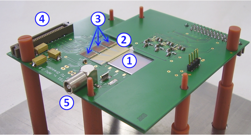
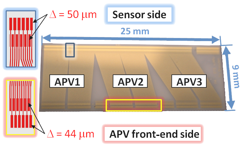
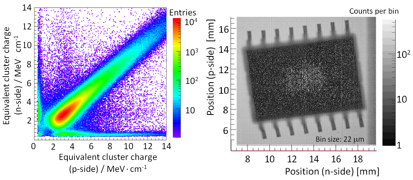
A photograph of the completed detector module is shown in figure 4.18. The sensor is glued to L-shaped circuit boards thus allowing a double-sided readout with one common design. A ceramic pitch adapter has been fabricated, which leads from the readout pitch of the sensor to the needed structure of the APV25 \frontendchip with a pitch of just 44 m. One photograph of the fabricated pitch adapter can be found in figure 4.19 along with the schematics of the pad geometry.
Extended studies with a series of detector modules have been performed proving the full functionality of the setup. Moreover, there are no indications of an impact of the assembly procedure on the final detector performance. Selected results of the measurements are collected in figure 4.20.
References
Chapter 5 Infrastructure
5.1 Optical Data Transmission
The maximum expected data rate for the pixel MVD is estimated to
be 450 Mbit/chip. The 8b/10b encoding on the output data could increase the number to 600 Mbit/chip.
Due to the absence of a trigger signal, no trigger matching logic can be
used to reduce the amount of data already at the \frontendchip level. Moreover,
the track distribution over the barrel and the disks can vary significantly
depending on the type of the target, thus not allowing an optimisation based
on the detector position. These constraints make the pixel MVD data transmission
extremely demanding in terms of required bandwidth.
Another stringent constraint is due to the reduced dimensions of the MVD and its
closeness to the interaction point, which limits the number of cables that can
be accommodated and tolerated (for material budget issues).
These constraints lead to the choice of using high speed serial links and to
convert the data transmission from electrical to optical as close as possible
to the detector, in order to profit from the high data rates allowed by the
optical fibers.
Unfortunately the use of off-the-shelves components for this application is
not straightforward because of the radiation environment where the components
will be placed. However, the problem is common to most of the HEP community
and in particular for the upgrades of the LHC experiments. In this context
two research projects, named GigaBit Transceiver (GBT) [Moreira09] and
Versatile Link (VL) [Troska09] are ongoing in order to develop a radiation
tolerant transceiver (the GBT) and to qualify optical components for the radiation
environment (the VL).The connection between the MVD and the DAQ is going to make
profit of this development and therefore to design a \frontendelectronic compatible
with the GBT interface. Figure 5.1 shows the scheme proposed by the
GBT and VL projects.
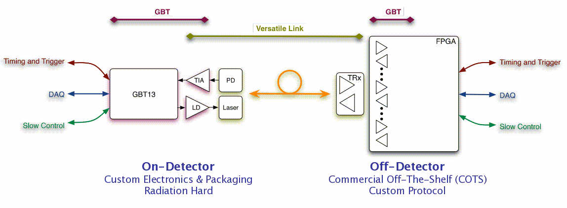
5.1.1 GigaBit Transceiver
The goal of the GBT project [Moreira09] is to produce the electrical
components of a radiation hard optical link, as shown in figure 5.1.
One half of the system resides on the detector and hence in a radiation environment,
therefore requiring custom electronics. The other half of the system is free from
radiation and can use commercially-available components. Optical data transmission is
via a system of opto-electronics components produced by the Versatile Link project.
The architecture incorporates timing and trigger signals, detector data and slow controls
all into one physical link, hence providing an economic solution for all data
transmission in a particle physics experiment.
The on-detector part of the system consists of the following components.
-
•
GBTX [Moreira11] [Cobanoglu09]: a serialiser-de-serialiser chip receiving and transmitting serial data at 4.8 Gb/s . It encodes and decodes the data into the GBT protocol and provides the interface to the detector \frontendelectronics.
-
•
GBTIA [Menouni09]: a trans-impedance amplifier receiving the 4.8 Gb/s serial input data from a photodiode. This device was specially designed to cope with the performance degradation of PIN-diodes under radiation. In particular the GBTIA can handle very large photodiode leakage currents (a condition that is typical for PIN-diodes subjected to high radiation doses) with only a moderate degradation of the sensitivity. The device integrates in the same die the transimpedance pre-amplifier, limiting amplifier and 50 line driver.
-
•
GBLD [Mazza09]: a laser-driver ASIC to modulate 4.8 Gb/s serial data on a laser. At present it is not yet clear which type of laser diodes, edge-emitters or VCSELs, will offer the best tolerance to radiation [Troska09]. The GBLD was thus conceived to drive both types of lasers. These devices have very different characteristics with the former type requiring high modulation and bias currents while the latter need low bias and modulation currents. The GBLD is thus a programmable device that can handle both types of lasers. Additionally, the GBLD implements programmable pre- and de-emphasis equalisation, a feature that allows its optimisation for different laser responses.
-
•
GBT-SCA [Gabrielli09]: a chip to provide the slow-controls interface to the \frontendelectronics. This device is optional in the GBT system. Its main functions are to adapt the GBT to the most commonly used control buses used HEP as well as the monitoring of detector environmental quantities such as temperatures and voltages.
The off-detector part of the GBT system consists of a
Field-Programmable-Gate-Array (FPGA), programmed to be
compatible with the GBT protocol and to provide the interface
to off-detector systems.
To implement reliable links the on-detector components
have to be tolerant to total radiation doses and to single event
effects (SEE), for example transient pulses in the photodiodes
and bit flips in the digital logic. The chips will therefore be
implemented in commercial 130 nm CMOS to benefit from its
inherent resistance to ionizing radiation. Tolerance to SEE is
achieved by triple modular redundancy (TMR) and other
architectural choices. One such measure is forward error correction (FEC),
where the data is transmitted together with a Reed-Solomon code which allows
both error detection and correction in the receiver.
The format of the GBT data packet is shown in figure 5.2. A
fixed header (H) is followed by 4 bits of slow control data
(SC), 80 bits of user data (D) and the Reed-Solomon FEC
code of 32 bits. The coding efficiency is therefore 88/120 = 73%,
and the available user bandwidth is 3.2 Gb/s.
FPGA designs have been successfully implemented in
both Altera and Xilinx devices, and reference firmware is
available to users. Details on the FPGA design can be found
in [Baron09].
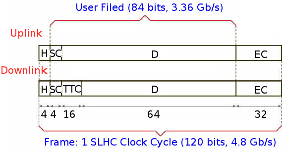
5.2 Off-Detector Electronics
The \pandaDAQ System architecture defines 3 multiplexing and aggregation layers, before the detector data are sent to the Level 1 Trigger farm implemented by the Compute Nodes in ATCA crates. The first layer does the multiplexing of several \frontendinput links into one outgoing link. In addition to this, information on beam structure (2 bursts and 500 super bursts) and global clock is received by the SODA system and propagated to the \frontendmodules in order to provide proper time-stamping of the detector data. In two further aggregation stages data are grouped into data blocks corresponding to one burst and super blocks corresponding to one super burst.
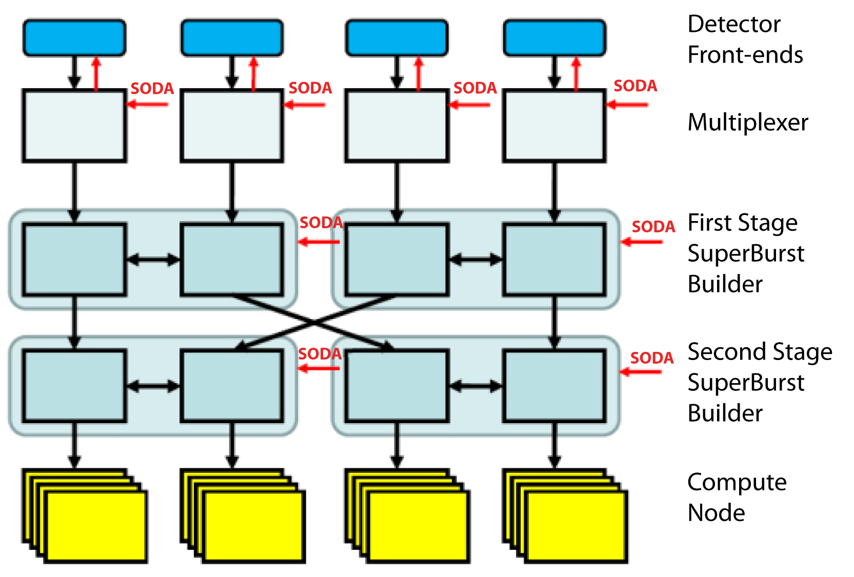
Due to its extreme data rates the MVD provides high challenges for this architecture. Assuming that the MVD module controllers and service boards (with the GBT) are combined such that the GBT links are almost fully loaded, the MVD Multiplexer Boards (MMBs)will do a 3-to-1 multiplexing with 3 optical links from the GBTs on the service boards and one optical uplink with 10 Gb/s. Since the maximum user data rate for the GBT is 3.28 Gb/s, all three links from the service boards can be fully loaded, simultaneously. Due to the high output rate the MMBs will be designed as MicroTCA-Boards. This allows direct insertion into the Compute Node version 3 and skipping of the SuperBurst building stages. Implementation of test systems is supported, as well.
The MMB will not use the GBT, but will implement the GBT protocol with a commercial FPGA. The Xilinx Virtex 6 is foreseen for this purpose, but the final decision will be done during the hardware design phase. Figure 5.4 shows the main components of the MMB. SODA provides global clock and timing as well as information on bursts and super bursts, which will be propagated by the FPGA via the optical links to the service modules using the trigger&timing interface component of the GBT. This information in combination with the reference clocks and reset pulses generated by the GBT allows proper time stamping of the FE ASIC data. Via the FPGA the GBT-SCA is accessible in order to do environmental monitoring. Setting the parameters of the FE ASIC (e.g. thresholds) is done via the DAQ interface of the GBT and not with the GBT-SCA. On the MicroTCA interface the PCIe protocol (with 4 lanes) is used in the fat pipe. The PCIe protocol is implemented by the FPGA and gives access to the above-mentioned management and control functions. Also the detector data can be sent via the MicroTCA interface instead of the optical uplink. In this case, the average load over all 3 links from the GBTs must not overcome 80%. The module management controller (MMC) is implemented by a Microcontroller, which communicates with the shelf manager via I2C.
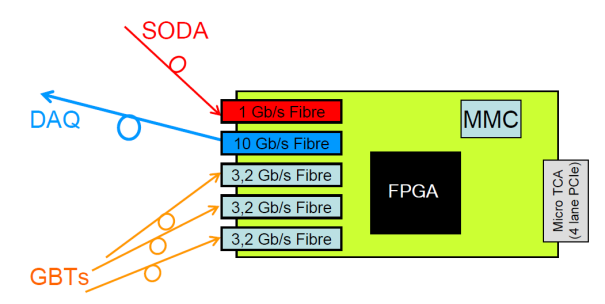
In normal operation it is foreseen that the MMBs will reside in MicroTCA crates. Each MicroTCA crate will contain one commercial off-the-shelf CPU-board for management and control purposes. Linux will run on the CPU-board enabling comfortable local and remote access to the MMBs via the PCIe link on the MicroTCA backplane. The shelf-monitoring functions of MicroTCA support additional remote monitoring and control operations.
5.3 Power Supply System
5.3.1 Introduction
The power supply system for the whole MVD has to provide low voltage for a total number of 2130 readout circuits, including pixel and strip electronics, and 346 controller or transceiver circuits to transmit the data towards the DAQ.
Besides the power supply system has to provide high voltage for a total number of 136 super modules, including both pixel and strip sensors.
5.3.2 Powering Concept for the Pixel Part
For the hybrid pixel part the smallest unit considered for the segmentation of the power supply system is a super module, that can include up to 6 readout chips (ToPix) and a transceiver chip (GBT). For each basic unit, the design of the power supply system has to provide two independent floating channels, for the analogue and digital sections, with sensing feedback, for the voltage compensation due to the cable voltage drop.
With respect to the power supply system, the requirements for the ToPix readout chip are: a channel for the analog circuits with a nominal voltage V, an upper voltage limit V, a nominal current mA, an upper current limit mA; and a channel for the digital circuits with a nominal voltage V, an upper voltage limit V, a nominal current A, an upper current limit A. These numbers are evaluated after the measurement on the ASIC prototype ToPix v3, and extrapolating the result to a full size chip with the complete array of cells, that affects mainly the analogue current, and the entire set of columns, that affects the digital current. A significant amount of the digital current is due to the differential drivers (7 outputs) and receivers (9 inputs) constituting the interface for the chip that, at present, is considered completed and does not require to be increased as in the case of the current for the end of column blocks. Currently, the expected currents are evaluated considering a readout circuit running with a system clock 160 MHz fast and a pre emphasis capability to drive the long transmission lines, while working at 80 MHz or releasing the boosting could decrease the total current consumption of the 20% or 5% respectively. Therefore, sensible current limits for the power supply have to be selected to protect the readout, without requiring too much power that could lead to an oversised system; for this purpose, since the present figures constitute the worst case, an increment of just 10% for all the parameters has been chosen.
Power Regulators
As power regulator the linear regulator solution has been excluded due to the low efficiency in the power conversion, while a switching DC-DC solution has been chosen because it has an higher efficiency and can be based on the project currently under development at CERN for the upgrade of the LHC experiments.
The switching converter needs to store the energy either by the magnetic field (using inductors) or by the electrical field (using capacitors); at present the main project is addressing the architecture with inductors that allows larger efficiency, although the architecture with capacitor looks very attractive due to the small size of the whole circuit. The full DC-DC converter is a kind of hybrid based on a small PCB containing few passive components, mainly the inductor, and an ASIC providing the switching transistors and the control logic to monitor the correct behaviour [ref:dcdc]. Currently there are different prototypes featuring integrated circuits made with different technology to test their hardness with respect to the radiation dose, but in any case all of them foresee an input voltage around V, an output voltage V compatible with the new readout circuits and an output current of roughly A.
This type of inductor based converter, also called “buck converter”, requires particular care when working in a high magnetic field and for this reason it cannot make use of ferrite core coils since it risks the saturation, but an air core coil is preferred although an increment in the size is expected. Another issue related to the inductor is the radiated switching noise and his electromagnetic compatibility with the system, for this purpose the coil is shielded by a small box with the conductive surface and the geometrical dimensions become in the order of .
At present the CERN development is selecting the best technology for the ASIC production from the point of view of the radiation hardness, but a backup solution has been found in the 350 nm On Semiconductor that has been already qualified for this application. The other technology option comes from the 250 nm IHP, but since it is a more advanced solution it has not yet reached the necessary level of radiation hardness and it isn’t enough tolerant against the single event burnout or the displacement damage. Specifically these DC-DC converters have been tested to cope with the environment of an experiment for high energy physics considering a total integrated dose of around 1 MGy, a particle fluence of roughly \neueqand a magnetic field of about 4 T.
5.3.3 Powering Concept for the Strip Part
For the strip part the foreseen powering scheme for one super module contains separate low voltage supply paths for the n-side and the p-side readout electronics, respectively since the n-side \frontendelectronics is operated without galvanic reference to a common ground in a floating regime. This avoids high parasitic currents in the case of breakdown of the thin insulation barrier between n-side implants and metallisation (pinholes) of the sensors, which would otherwise result in the loss of the complete sensor. Thus a total of 4 independent low voltages (one analogue and one digital for either sensor readout side) and 4 high voltages for each sensor bias have to be supplied. The low voltage paths are connected with sense feedback to compensate for the voltage drop on the cables. Assuming a maximum of 1 W power dissipation per \frontendat an operation voltage of 3.3 V a value of 5.3 A can be estimated for the maximum supply current on the low voltage lines. The current drawn on the bias voltage lines is negligible even with the maximum applied irradiation dose at the end of the \pandalifetime and amounts to at most 2 mA per sensor. Sensing lines are thus not required for this supply but a good filtering with very low cutoff frequencies is mandatory on the module level.
5.4 Cables
A special feature of the \PANDAexperiment comes from the triggerless DAQ, that requires a very high output bandwidth because to the continuous flux of data that cannot exploit the de-randomisation coming from an external trigger at a lower rate. Besides, since at present the only way out from the MVD is in the backward region, the cabling becomes a serious issue because of the amount of material needed to take out all the data from the sensitive volume.
5.4.1 Requirements
Due to the average annihilation rate of 20 MHz a flux of particles per second and chip is expected in the hottest region, the forward disks. The current design for the pixels considers a ToPix readout circuit managing a 100 m thick sensor, a data word of 40 bit per event, a variable luminosity structure due to the peak in the beam profile and the crossing of the pellet target, therefore the readout chips in the middle of the disks have to deal with a data rate of 450 Mbit/s each.
The present solution for the architecture of the serial link comes from the Giga Bit Transceiver (GBT) project under development at CERN, for the upgrade of the experiments that will be running at the Super LHC (SLHC). The GBT is foreseen to be interconnected to the readout circuits by an Elink that is an electrical interface implementing a serial connection.
5.4.2 Signal Cable
To deal with the low material budget for the vertex region, the use of copper cables is excluded and one has to employ aluminium cables. In this case considering that aluminium has a lower atomic number than copper, even if it has a higher resistivity, an overall gain is obtained in the material budget because the aluminium radiation length is 88.9 mm instead of copper radiation length that is 14.4 mm.
From the physical point of view each logical signal going to, or coming from, ToPix chip is implemented by a differential pair to be less sensitive against the noise that can be induced at the same time on each single line, and that will be canceled after the subtraction between the two phases. In particular these connections are implemented as a transmission lines using the microstrip technique, and are composed as a sandwich of two aluminium conductive layers separated by a polyimide insulator layer [ref:cable]. On one side the two tracks composing the differential pair are laid down, while on the other side the metal plane constitutes the reference ground.
Al Prototypes
Several kinds of cable prototypes were made and tested, differing either in the manufacturing technology or in the physical layout. For the first choice the standard solution is a laminated sheet over an polyimide layer, that is worked in a way similar to a PCB etching the metal from the area where it must be removed.
The other manufacturing solution is an aluminium deposition on top of an insulator film, that is obtained dispensing the metal just in the required area defined by the layout pattern, by the Physical Vapour Deposition (PVD).
Folded Layout
The first samples were produced to test both the technologies, by using the metal lamination from the Technology Department at CERN and successively the aluminium deposition from the Techfab company near Torino. The CERN prototype has a stack of up to two aluminium foils with a thickness of 15 m, on both sides of the plastic film 51 m thick produced by DuPont under the commercial name of Pyralux. Various layout prototypes were produced with different widths and spacing of 100 m + 100 m, 150 m + 150 m and 200 m + 200 m respectively.
The Techfab prototype features a cross section of two aluminium depositions with a thickness of roughly 7 m, around the 50 m thick plastic sheet produced by DuPont as common kapton. In this case, a sample with a unique layout showing 150 m width and 150 m spacing has been obtained. Due to some issues with the wire bonding procedure, a try has been performed with an aluminium/silicon alloy to improve the bond strength. The samples with the folded layout have been used to perform an irradiation test by neutrons at the LENA nuclear reactor in Pavia with a total fluence greater than what is expected for the \PANDAlifetime, and no significant variations have been observed.
Straight Layout
The low mass cables have been designed implementing the connections as a transmission line, using the microstrip technique on DuPont materials and manufacturing them in a way similar to a PCB. Currently there are aluminium microstrips, produced by the Technology Department at CERN, with a layout including 18 differential pairs for a total number of 36 tracks; at present there are two versions differing for the nominal width that is 100 m or 150 m and the spacing that is 100 m or 150 m respectively. All of them have the insulator cover on the bottom side to protect the ground plane, while one more parameter introducing another difference on the available samples is the presence or the absence of the insulator cover laid on the top side where the differential strips are implemented (figure 5.5). Summarising, at present, there are 4 different kinds of aluminium microstrips 1 m long under study differing for the pitch size or for the top covering.
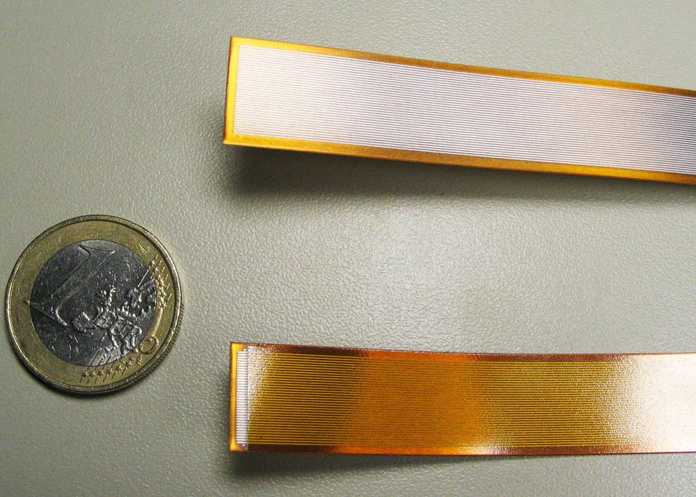
Results
From a static point of view the aluminium microstrips were tested to measure the resistance of each track between its ends, and the capacitance referenced to the ground plane; moreover the uniformity for these parameters was evaluated (figure 5.6).
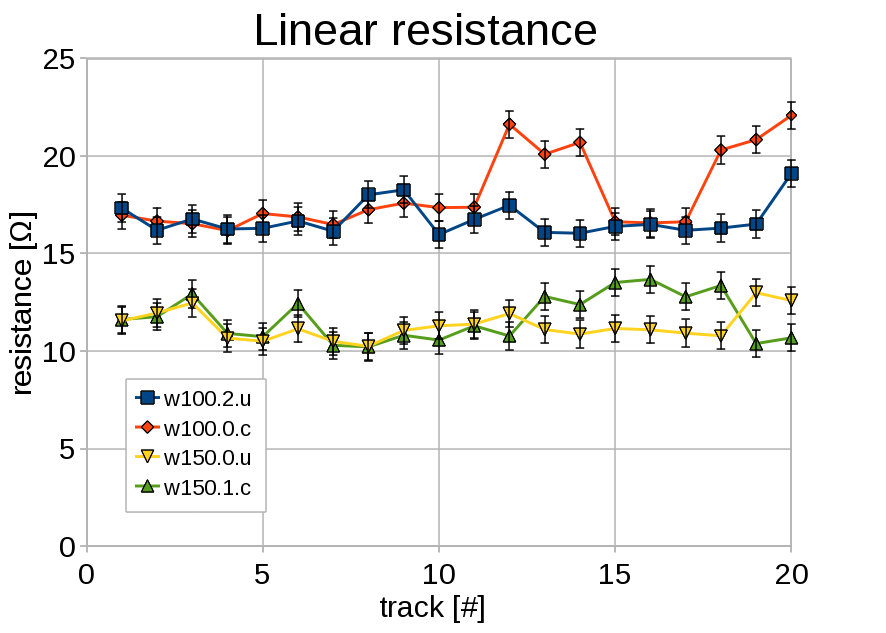
The measurement has been performed bonding both cable ends to the test station to reduce the contact problems, and no dependence between static parameters and track position has been observed. Instead, as expected, the results show that there is a clear relation between the linear resistance and the track width, that is around 12 for the large strips (150 m) and about 17 for the narrow ones (100 m). Regarding the dynamic behavior, a test bench has been setup with some prototype circuits implementing the Scalable Low Voltage Signaling (SLVS) standard, to measure the total jitter and its main components like the deterministic jitter or to perform a Bit Error Ratio Test (BERT) as a function of the data rate [ref:slvs]. Other tests were performed to evaluate the cross talk effect with the transceiver prototypes, and to measure the total jitter produced by just the aluminium cables without introducing the component due to the SLVS circuits. The present solution considers that signals running on the low mass cables comply with the SLVS differential standard which foresees for each line a mV and a mV, against the LVDS differential standard which typically foresees for each line a V and a V. The setup for the measurement is composed of the aluminium cable under test that is glued by the shield on two boards specifically designed, while the interconnections are made with a standard wire bonding. The test was performed by a pulse generator configured to produce a Pseudo Random Bit Sequence (PRBS) with a pattern length of bits, and output levels according the SLVS standard. In this way the performance of the aluminium microstrip can be evaluated studying the analog shape of the signals coming out of cable, without the insertion of any distortion attributable to the transceivers. The 4 samples measured so far are called w100.0.c, w100.2.u, w150.0.u and w150.1.c where the first number represents the track width in micrometer, and the last letter represent the condition to be covered or uncovered with the insulator film. The total jitter has been measured and evaluated in Unit Interval (UI), that represents the ideal period of a bit irrespective of the link speed, allowing the relative comparison between different data rate (figure 5.7). Since the commercial serialiser and deserialiser are considered safe when their total jitter came up to a threshold of UI, it is possible to conclude that the aluminium microstrips with track width m are able to run up to a data rate Mbit/s while the differential cables with track width m can work up to a data rate Mbit/s.
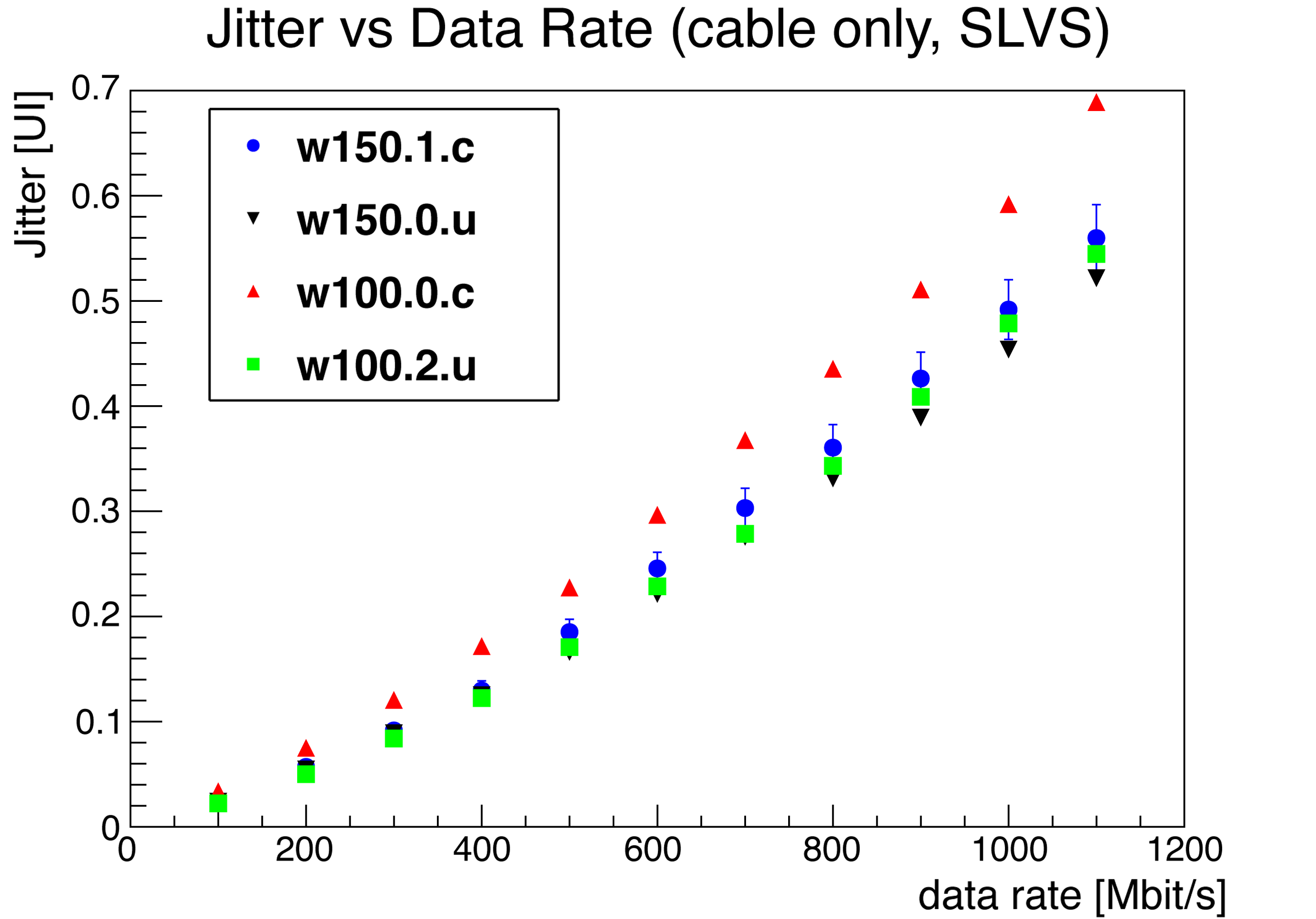
An useful tool to evaluate the total jitter with respect to the unit interval is the eye diagram, see figure 5.8, that is a composite view of the signal made by the overlapping of many acquired waveforms upon each other corresponding to bit periods representing any possible logic states and transitions.
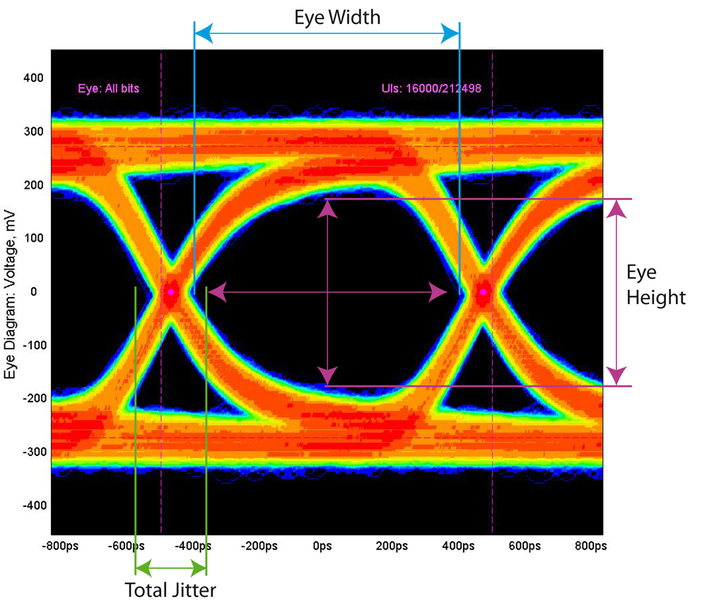
Moreover, analysing the eye diagram height at the end of the flexcable relative to the input PRBS, the differential amplitude can be evaluated and it results in final value of roughly 300 mV instead of the nominal value of about 400 mV, with an attenuation that is due to the tracks linear resistance. The test setup has allowed an evaluation of the cross talk keeping a victim differential pair biased in a steady state and driving the aggressor differential lines, on the left and right sides of the first one, by the same signal, but a very light effect has been reported and probably this is due to the little swing of the SLVS standard and the relatively low transition time of the signals connected to the high capacitive load.
5.4.3 Power Cable
Each ToPix circuit is expected to consume around 1.4 A and since it requires a supply voltage at 1.2 V, that means a total power of 1.68 W typically, corresponding to a relative power of 979 mW/cm2. However two independent lines have to be distributed from the power converter to separate the analog part from the digital part, to reduce the risk of mutual interference.
Also in this case the material budget requirement represents a constraint that prevents the use of copper conductors inside the active volume of the MVD, then a solution with aluminium was investigated. At present a sample of enameled wire made of copper clad aluminium has been evaluated to verify that it is suitable for the routing in a very limited space, reducing the voltage drop to roughly 100 mV.
5.5 Mechanical Structures
The whole MVD is composed by four mechanically independent sub-structures:
-
•
pixel barrels;
-
•
pixel disks;
-
•
strip barrels;
-
•
strip disks.
Each of them is assembled independently, then gathered on a stand and positioned on a holding frame. Figure 5.9 shows a longitudinal cross section of the MVD together with the cross-pipe sector.
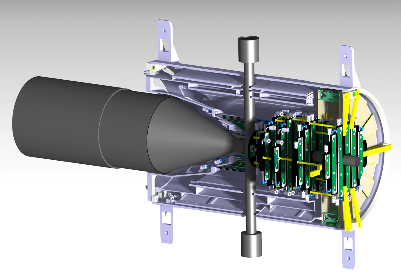
5.5.1 Global Support: The Frame
The frame is the main structural element of the whole MVD. Its purpose is to suspend and keep in position all the sub-structures, with a relative positioning error of less than 100 m as well as to connect the MVD to the external world (i.e. the central tracker). The frame also acts as support for the services from the inner part of the MVD. The frame has a sandwich structure, made by a high modulus composite of unidirectional carbon fiber cyanate ester resin and foam as core material. The cyanate ester resin systems feature good behavior and high dimensional stability when immersed into a temperature-humidity varying field. The use of a conventional epoxy system would have drawbacks, due to excessive moisture absorption and residual stress. As compared to epoxies, cyanate ester resins are inherently tougher, and they have significantly better electrical properties and lower moisture uptake [re:mechRef_1] [re:mechRef_2]. The main properties of the M55J/LTM110-5 composite material are reported in table 5.1.
| Tensile Modulus (GPa) | 310 |
| Tensile Strength (MPa) | 2000 |
| Poisson’s ratio | 310 |
| CTE fibre (ppm/∘C) | |
| CTE resin (ppm/∘C) | 60 |
| Moisture uptake (155 d - 22∘C - 75% RH) | 1.4% |
A finite elements analysis has been performed in order to define the minimum number of plies necessary to achieve the requested stiffness. According to the simulation, the frame has been designed including two skins, each composed of four plies with a quasi-symmetric stacking sequence of unidirectional M55J carbon fiber prepreg, and 3 mm of Rohacell®51IG as core material. A set of eight semi-circular, 1 mm thick, reinforcing ribs is embedded into the structure. These ribs will be realised with the same composite material used for the external skins. The final thickness of the frame is 4 mm.
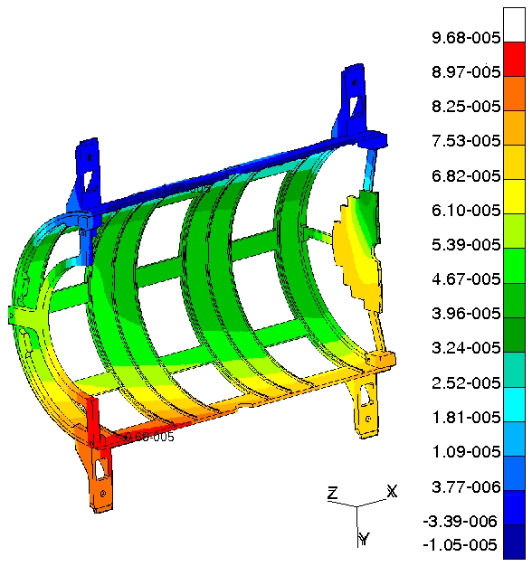
Figure 5.10 shows the behavior of the frame under gravitational load. Extra loads are applied, distributed on the end-rings to take into account a safety factor of 2. The simulation shows a maximum displacement in vertical direction of less than 100 m.
The frame holds the four sub-structures containing the silicon devices in their place. Two rings glued at the ends of the frame act as connectors between the sub-structures and the frame itself. The rings are made of mattglass/epoxy laminate composite, Durostone®EPM203, pre-machined and finished after gluing in order to achieve the final dimensions and the requested accuracy. A set of proper tools is necessary for these operations.
The relative position of the two halves is ensured by means of a three cam system. Figures 5.11, 5.12 and 5.13 show the ancillary components of the system. Two cylindrical cams are located on the upper ends of one half frame, whereas a third one is located at the lower end. A sphere is positioned on top of the cams. On the other half frame there are inserts, which are embedded into the rings. One insert, on the top, has a “V” shape while a second one, also on the top but at the opposite end, is “U”-shaped.
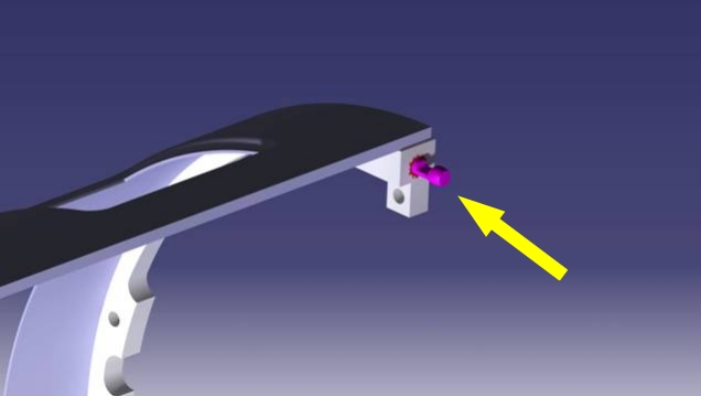
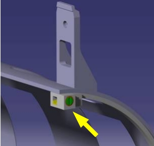
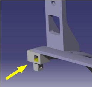
The upper cams pass through the inserts and fix the position along the Z axis. The third cam, located on the bottom of the half frame, fixes the radial position. All the ancillaries are made by hardened aluminium alloy (Hotokol). A similar system allows the MVD to be suspended from the Central Frame and to be fixed with three springs. The springs are shaped so to get a two-components locking force: one component (X) is on the horizontal plane fixing the radial position, while the second is on the vertical plane, downward oriented, and defines the Y and Z components. Finally, the position is achieved by means of the V and U shaped inserts embedded into the Central Frame structure.
This system allows the control of the position to be achieved, so that re-positioning is possible with a high degree of accuracy, that we can evaluate to be less than 10 m [re:mechRef_3].
5.5.2 The Pixel Support Structure
Pixel Barrels
The pixel barrels are a collection of two cylindrical layers of detectors placed around the interaction point and coaxial with the beam pipe axis.
The first, innermost, layer is composed by 14 super-modules, while the second layer by 28. Each super-module is a linear structure of pixel sensors, hosting from two to twelve elements, glued on a mechanical support made of a carbon foam (POCO HTC and POCO FOAM) thin layer and a -shaped substrate realised with a M55J carbon fibre cyanate ester resin composite. The cooling tube is embedded between the carbon foam and the substrate.
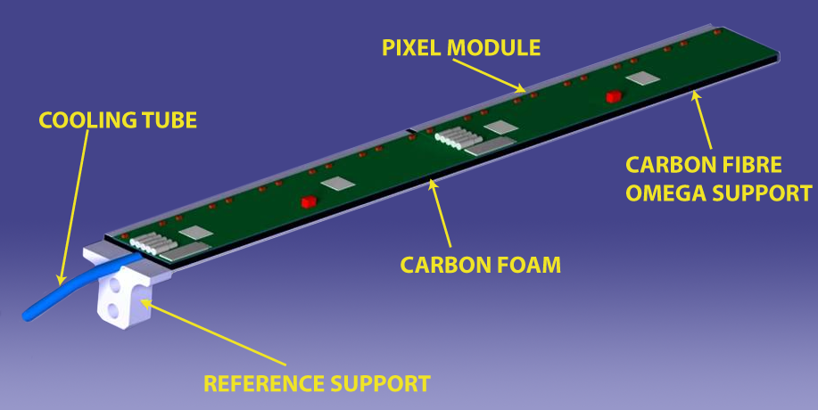
A plastic block, glued on one end of the substrate, acts as reference. The block has two precision holes through which two precision screws fasten the super module to the support structure.
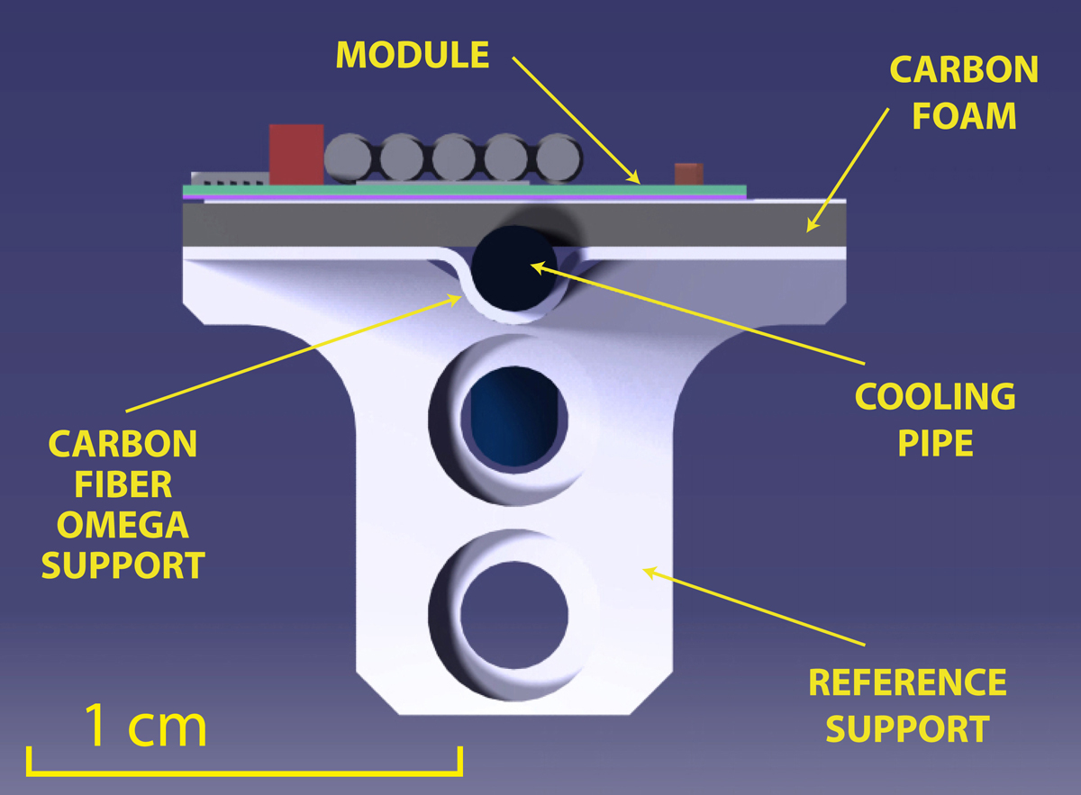
The support structure is an assembled set of sub-structures. Due to the strong geometrical constraints, the shape of the support structure is formed by the surfaces of two semi-truncated cones interconnected by two reference rings. The reference rings contain the positioning holes for the super-modules and allow the precise positioning of the detectors.
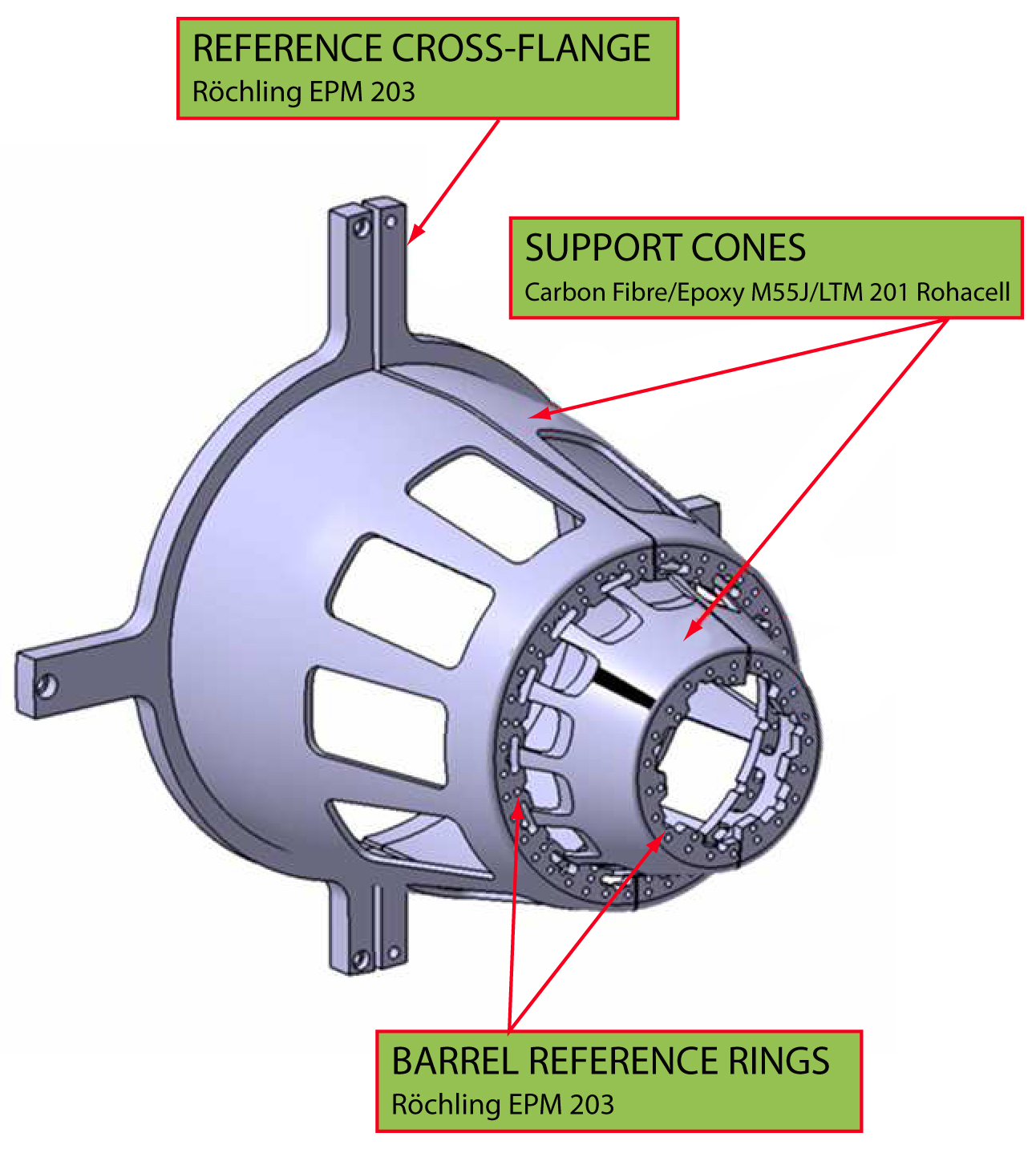
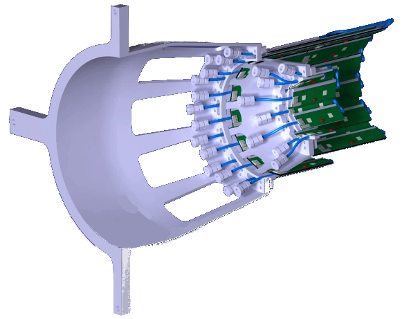
The support structure, shown in figure 5.16 is suspended from the frame by a reference cross flange. In figure 5.17 the half barrel of the second layer of pixel is shown assembled on the cone support. In each barrel the staves are arranged at two different radius and the overlap of the active areas is 0.3 mm.
Pixel Disks
The disks are six planar structures arranged at different distances from the interaction point. Each disk is divided vertically in two parts, called half disks. In this way it is possible to assemble the whole set around the pipe. Each disk is composed by a planar support structure, by detectors modules and by cooling tubes. The carbon foam planar structures also act as cooling bridges. The cooling tubes are embedded into the disks while the detectors modules are glued on both sides of each disk in order to get the largest possible coverage.
The carbon foams, both the POCO HTC and the POCO FOAM, are supplied in rectangular plates. Typical dimensions are . With the goal of cutting the shapes for both, the barrel elements and the disks elements, in the most efficient way, with minor possible machine rejection in mind, different production methods have been investigated. The most efficient way is to cut the shapes from the carbon foam plates with wire EDM.
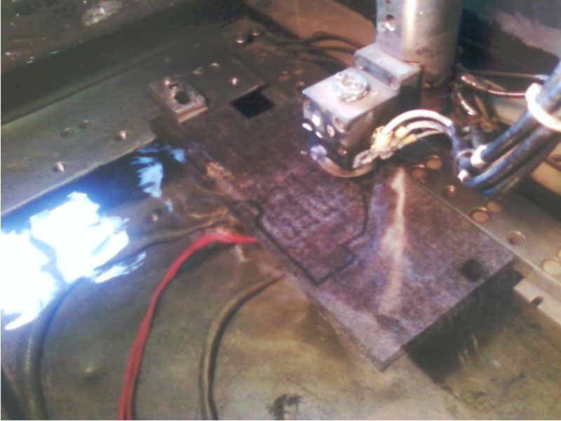
As general philosophy the shapes are cut from the plate (figure 5.18) and subsequently sliced-up (figure 5.19).
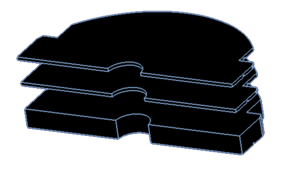
The wire EDM operates with the material to be cut immersed into water. The foam acts as a “sponge”. After the wire cut a big quantity of water was embedded into the foam element. In order to remove the water absorbed, the element was ´baked¡ in an oven for 48 hours at 60 ∘C. Before the baking the foam element weight was 15.12 g, while after 48 hours of baking the weight became 13.12 g, as expected for the dry element.
The set of six half disks is assembled to obtain a half forward pixel detector (see figure 5.20). The relative distances between disks are ensured by spacers, glued on the disk surfaces. The final position of each half disk is surveyed and referred to a set of external benchmarks fixed on a suspender system, which fastens the half forward detectors to the frame as well.
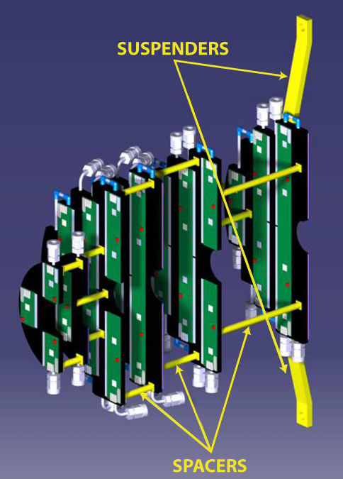
5.5.3 Support Structures of the Strip Part
Strip Barrels
The main holding structure of the strip barrel part consists of two half-cylinders with a radius of 11.4 cm and an overall length of 49.3 cm. They are made out of a sandwich structure of two layers of carbon fibers (M55J) with a thickness of 0.2 mm each and a 2 mm core of Rohacell foam. These half-cylinders are attached to the global support structure of the MVD via 4 connectors at the upstream end of the detector (figure 5.22). Sawtooth shaped structures on the inside and the outside form a support surface for the sensor elements sitting on so called super-modules. A super module consists of four 6 cm long sensor modules and one or two short modules with a length of 3.5 cm. In addition a super module houses the readout electronics, interconnections, and the cooling system. The support structure is made out of the same sandwich structure used already for the support cylinders. Underneath the readout electronics the Rohacell core is replaced by a carbon foam (POCO HTC) with high thermal conductivity and an embedded cooling pipe of 2 mm diameter. The edges of the structure are bent to increase the stiffness of the structure (figure 5.23). The fixation of a super module on the sawtooth rings is done via special bearing points which allow a precise positioning and a compensation for different thermal expansion coefficients. The overall concept is based on the ALICE ladder repositioning system with a precision better than 6 m [re:mechRef_3].
Strip Disks
The two forward disks are made of two double layer half-disks, which are separated along the vertical axis. They have an outer radius of 137 mm, an inner radius of 75 mm and a spacing of 70 mm between them. The basic building block of the double-disk is a module which consists of two wedge shaped sensors which share a common PCB for the readout electronics and the cooling pipes. They are connected to a carbon foam sandwich structure which holds the sensors, the PCB, the two cooling pipes and does the connection to a support ring which sits at the outer rim of the disks. This support ring is then connected to the global support barrel of the MVD (figure 5.21).
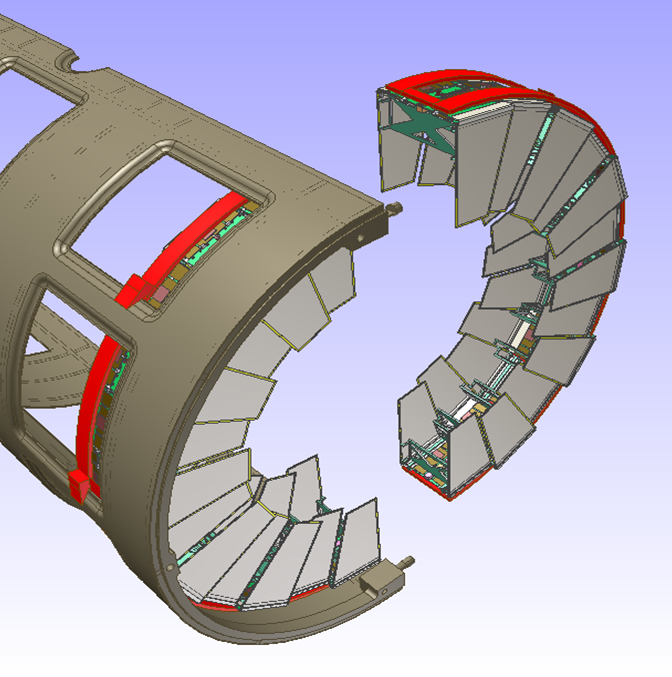
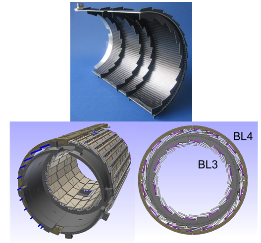
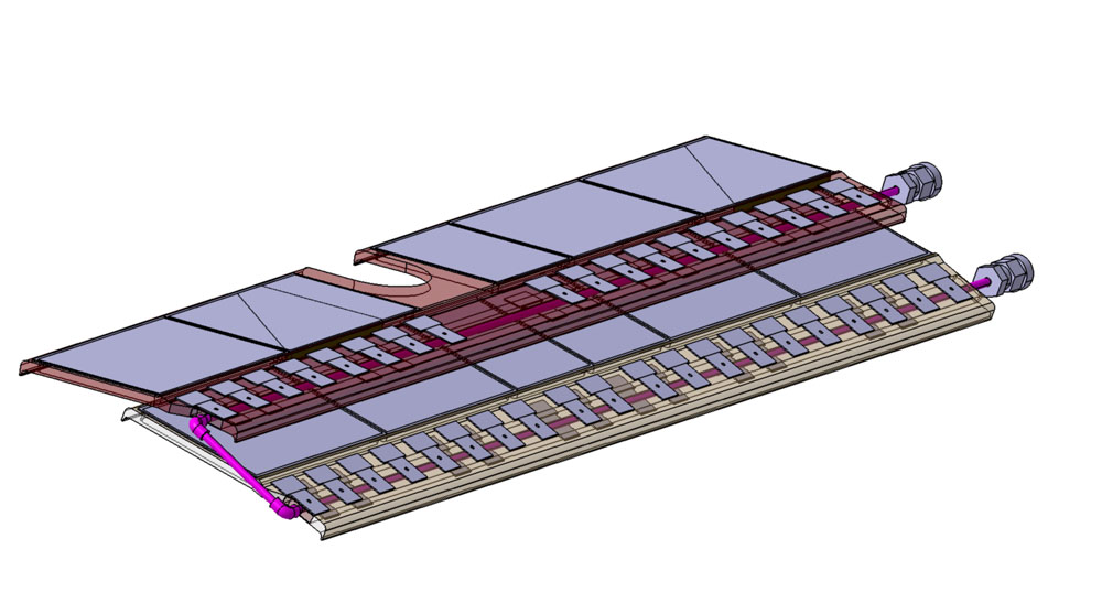
5.6 The Cooling System
The cooling system project provides to operate close to room temperature, with the temperature of the cooling fluid above the dew point. The difficulty in retrieval of the most appropriate coolant for the required operating temperatures and at moderate pressures, led to discard evaporative solutions, in favor of a depression system, using water as cooling fluid at 16 ∘C. A depression system should avoid leaks and reduce vibrations and stress on plastic fittings and manifolds, because of moderate pressure.
For geometry constraints and installation procedure, the MVD structure is divided in two halves, which will be connected together after target pipe installation. In addition, due to the MVD collocation relatively to the beam and target pipes, all the services and cooling pipes are routed from the upstream side. These constraints have conditioned the cooling design, which, always with the view to saving material, has made use of U-shape tubes, to avoid aimless material for the return lines and to reduce the number of cooling tubes. For an efficient cooling system, it is advisable to work with a turbulent regime flow, which means, considering an inner diameter of 1.84 mm for the cooling pipes and water as cooling fluid, with flow rates higher than 0,25 l/min. In a depression mode system, the pressure drops in the pipes are limited, confining cooling mass flows in reduced adjusting ranges. In fact the part provided with the pressure starts just near the MVD, in the inlet pipe, till the end of the cooling line (at the cooling plant, about m far from MVD). Pressure sensors on inlet (and return) lines ensure the depression mode in the MVD volume.
5.6.1 The Pixel Cooling System
The pixel volume of the Micro Vertex Detector (see figure 5.24 consists of a cylinder of 300 mm in diameter and 460 mm in length, in which 810 readout chips dissipate 1 W/cm2 for a total power of about 1.4 KW.
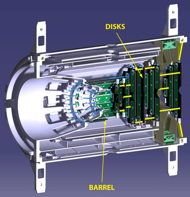
The main purpose of the cooling system is to guarantee the maximum temperature of the assembly under 35 ∘C. A dry air flow (nitrogen could be better) has to be foreseen in the MVD volume. For the cooling system design a material with low density, high thermal conductivity, low thermal expansion coefficient, machinable, gluable, stable at different temperatures and radiation resistant has been searched. The material which complied to all these requirements was the carbon foam: his open pore structure graphite produces a material with good thermal properties and low density. In table 5.2 and 5.3, density and thermal conductivity of two carbon foams, POCO HTC and POCO FOAM, are presented.
| POCO HTC | |
|---|---|
| Density | 0.9 g/cm3 |
| Thermal conductivity | |
| Out of plane | 245 W/() |
| In plane | 70 W/() |
| POCO FOAM | |
|---|---|
| Density | 0.55 g/cm3 |
| Thermal conductivity | |
| Out of plane | 135 W/() |
| In plane | 45 W/() |
Tests have been made on POCO HTC and on POCO FOAM to verify carbon foam thermal conductivity and mechanical stability at the radiation levels expected in the experiment. Using the TRIGA MARK II reactor in Pavia, five samples per foam type have been immersed in the reactor central channel at different reactor power, for a time of s, while one sample for foam type, not irradiated, was used as reference. The tests for the Young’s modulus estimation consisted on a carbon foam specimens ( and 5 mm of thickness), irradiated at different radiation levels, and then tensioned with a set of loads. For the evaluation of the deformation, strain gauges have been glued on the specimens and read by a HBM-MGCplus acquisition system. Test results are shown in figure 5.25 and 5.26. The carbon foam stiffness increases with the neutron fluence, the POCO FOAM Young’s modulus doubles in the considered irradiation range, while a 23% variation of the nominal value is observed for the POCO HTC.
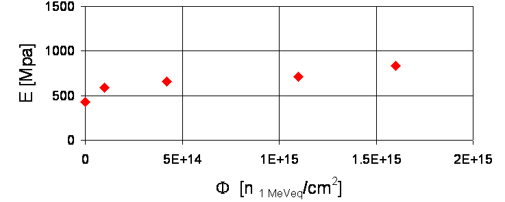
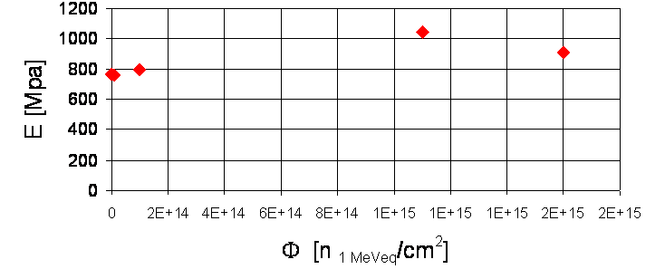
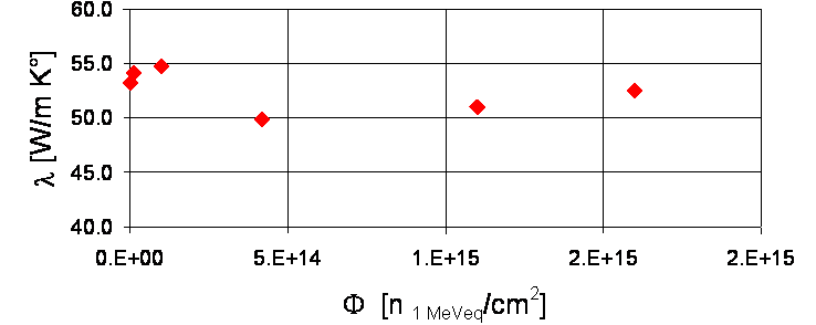
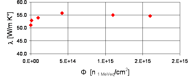
The tests for the thermal conductivity estimation consisted on the same carbon foam specimens heated on one side with a resistance and cooled on the other side. For the evaluation of the thermal conductivity, two thermocouples, arranged at a well known distance, have been glued on the specimens and read by the HBM-MGCplus acquisition system. The results of the thermal tests are reported in figure 5.27 and 5.28. the thermal conductivity variations are within 10% for both carbon foams.
The nominal values pre-irradiation have been used in the FEM simulations.
Test results show variation of the thermal conductivity values within 10%.
Because of different geometries, different chips concentrations, different
mechanical structure solutions, the cooling system design can be distinguished
in two sub-groups, the disks and the barrels.
Disk Cooling System
The cooling system for the disks consists of tubes of 2 mm external diameter, inserted in a carbon foam disk with a thickness of 4 mm, on which the detectors are glued on both sides. The tubes, with a wall thickness of 80 m, are in MP35N, a Nickel-Cobalt chromium-molybdenum alloy (by Minitubes) with excellent corrosion resistance and good ductility and toughness. In order to save material, to reduce pressure drops and to allow irregular paths to reach the manifolds of the first patch panel, the metal pipes are connected to flexible polyurethane tubes, [re:poli_tubes], through small plastic fittings (in ryton R4, custom made). The plastic fittings are glued on the metal cooling tubes with an epoxy glue (LOCTITE 3425), and all the connections are individually tested to ensure the pressure tightness. The disks group consists of two disks (4 halves) with a diameter of 75 mm, dissipating about 70 W (35 W each disk) and of four disks (8 halves), with a diameter of 150 mm, dissipating about 740 W (about 185 W each disk). On the small disks, due to space constraints, only one tube for each half disk is foreseen, while, for the bigger disks, three U-shaped tubes for each half, has been arranged. The U-tube is obtained with plastic elbows (in ryton R4, custom made) glued on the metal cooling pipes. In figure 5.29 and 5.30 the two kinds of half disks in carbon foam, completed of detector modules, cooling tubes and plastic fittings are shown.
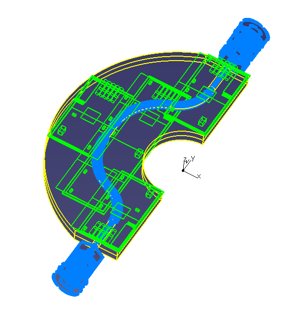
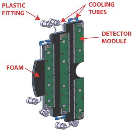
Finite Element Method (FEM) analyses, through temperature maps, allow fast evaluations of heat conduction, identifying the most effective solutions for the future prototype constructions. After a first prototype, useful to estimate the errors due to contact surface and to manual gluing, many FEM simulations have been performed to find out the thermally most efficient configuration of carbon foam and cooling pipes, considering different carbon foam thicknesses, tube diameters, tube numbers and cooling flow rates.
From FEM analyses it appears that the most effective operation to be applied is the doubling of cooling pipes.
The test on a second prototype validates FEM results. In figures 5.31 and 5.32 FEM analyses compared to test results are shown.
In figure 5.31 a FEM model with the real configuration of half disks, in carbon foam with a thickness of 4 mm, six cooling pipes, with pixel chips on both sides and a total power of 94 W, was used.
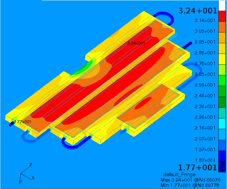
In figure 5.32, a FEM model with the dummy chips layout, simulating the pixel chips, dissipating 94 W, on the carbon foam disk with a thickness of 4 mm and six cooling pipes, was used.
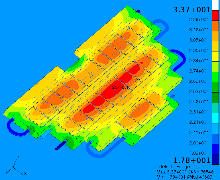
For both these FEM analyses, cooling water at 18.5 ∘C and flow rate of 0.3 l/min in each tube have been adopted. Figure 5.33 shows the disk prototype, in carbon foam, with six cooling tubes inside and 54 dummy chips (resistors).
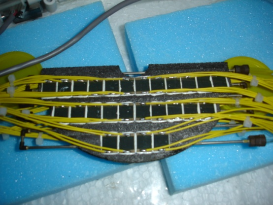
Figure 5.34 shows the test results, in line with FEM predictions. In this figure some hot spots are visible, due to manual gluing imperfections.
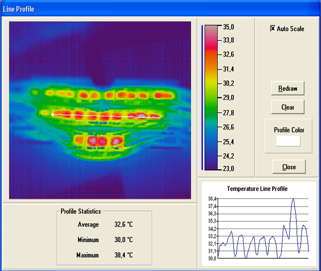
To guarantee a depression system, considering the pressure drops for the return lines, the pressure drops in the MVD line between the patch panel, in which pressure sensors can take place, must be limited and below mbar.
In the disks, to reduce the number of cooling circuits, it was thought to use S-shaped tubes, but the high pressure drop did not allow this solution.
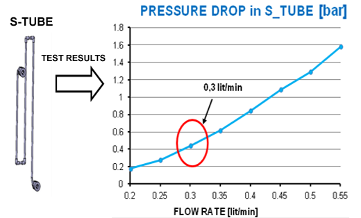
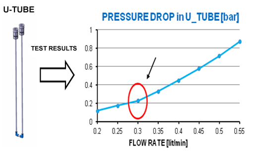
These measured pressure drops are referred to the only metal pipe, while the pressure sensors will be positioned in the patch panel manifolds, at least 1 m far from MVD and after plastic tubes connections. In the first case (S-shaped tube) the pressure drop is already close to the limit but all the path through plastic tubes and the manifolds is neglected. Therefore, the solution with S-shaped tubes cannot be adopted. On the other hand the U-shaped solution, thanks to its limited pressure drops, allows a more extended range of flow rate settings.
Barrel Cooling System
The cooling system is designed to drain the total power, about 75 W on the first layer and 500 W on the second, by 21 MP35N U-tubes (2mm of outer diameter and 80 m of thickness). The two halves of the layer 1, due to cooling constraints in use U-shaped tubes, cannot be symmetric: one half includes 8 staves and the other only 6.
Furthermore the barrel system, besides the drain of the heat dissipation, for the material budget limits, has to provide mechanical support. The system consists of the cooling tube inserted and glued in a sandwich of carbon foam and an Omega made by 3 plies of carbon fiber M55J (properly oriented). The high modulus of this carbon foam ensures the rigidity of the structure and, at the same time, acts as heat bridge for the cooling. The super module structure, which consists of the silicon detector, completed of chips, mechanical structure and cooling system, is shown in figure 5.14.
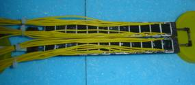
Even for the barrel part FEM analyses have been useful to find out the most efficient solutions and test results are presented below. Figure 5.37 shows the U-shaped cooling tubes in MP35N, with plastic fittings and plastic bends glued to the pipes. The chips are simulated by resistors, dissipating about 21 W in each stave. The cooling water for the test at 18 ∘C was fed with a flow rate of 0.3 l/min. The temperature map, shown in figure 5.38, was been obtained with a thermo camera (NEC thermo tracer).
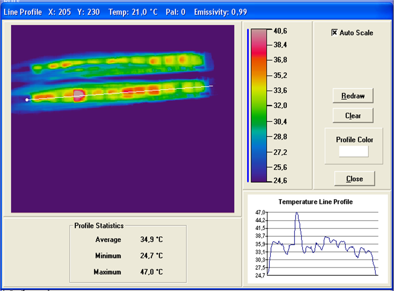
5.6.2 The Strip Cooling System
The strip part of the MVD is subdivided into a barrel section and a disk section. The barrel section again consists of two barrels with 552 \frontendchips needed for the inner one and 824 \frontendchips for the outer one. Compared to the numbers in table 2.5 these higher numbers consider the fall back solution of an individual readout for each sensor instead of a ganging of long strips for subsequent barrel sensors. The disk section consists of one double disk with 384 \frontendchips. Each of these \frontendchips consumes up to 1 W of power which sums up to a total power consumption of the strip part of 1.76 kW.
To cool away this power the same concept as in the pixel part is used. A water based system will be used which is operated in depression mode. Each support structure is equipped with a cooling tube of 2 mm diameter and a wall thickness of 80 m made out of MP35N. This cooling tube is glued with thermal conducting glue to a carbon foam material (POCO HTC) with excellent thermal conductivity which sits underneath the \frontendelectronics (see figure 5.39 for the strip barrel part).
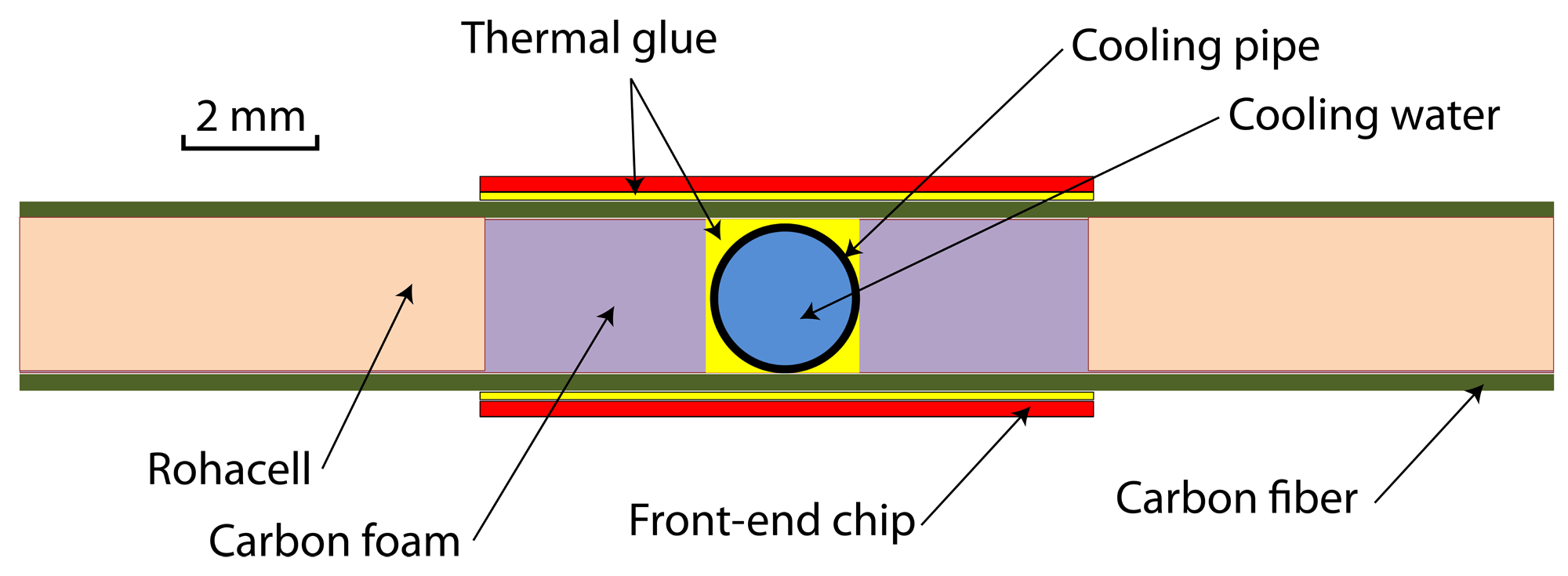
Detailed finite element simulations of different setups have been performed for the barrel part of the strip detector. The results of the best setup can be seen in figure 5.40. The maximum temperature the \frontendelectronics reaches is 32 ∘C in this setup. Almost all heat of the electronics is cooled away.
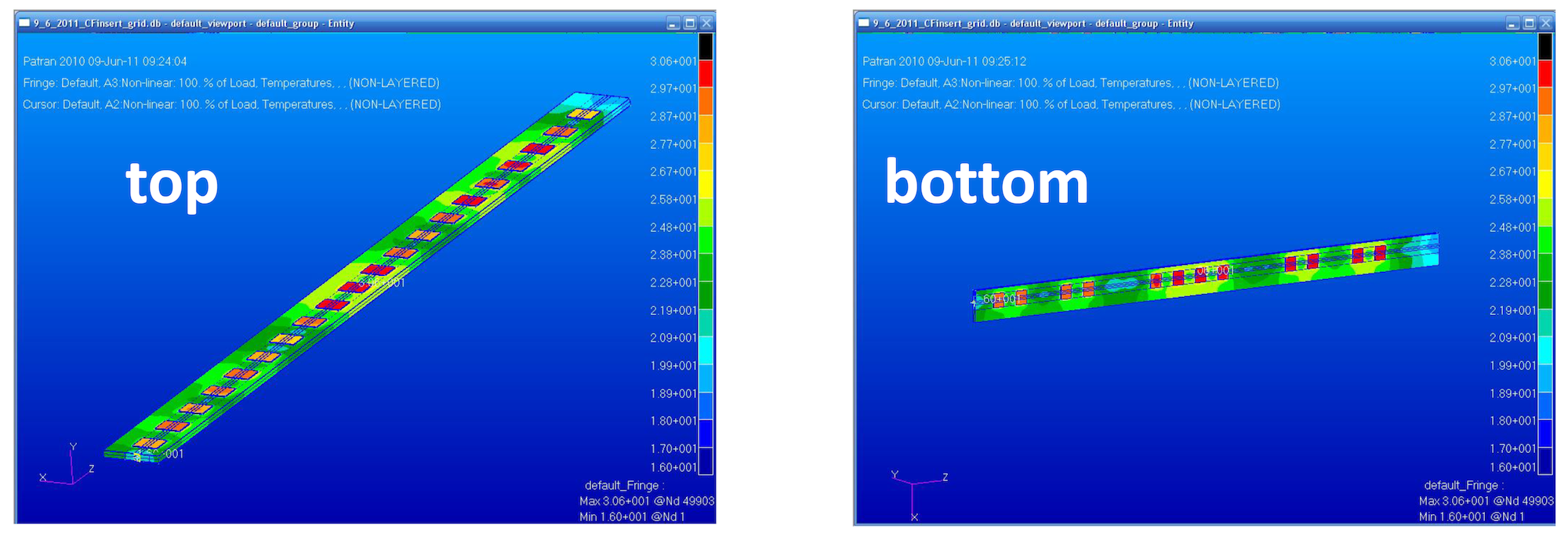
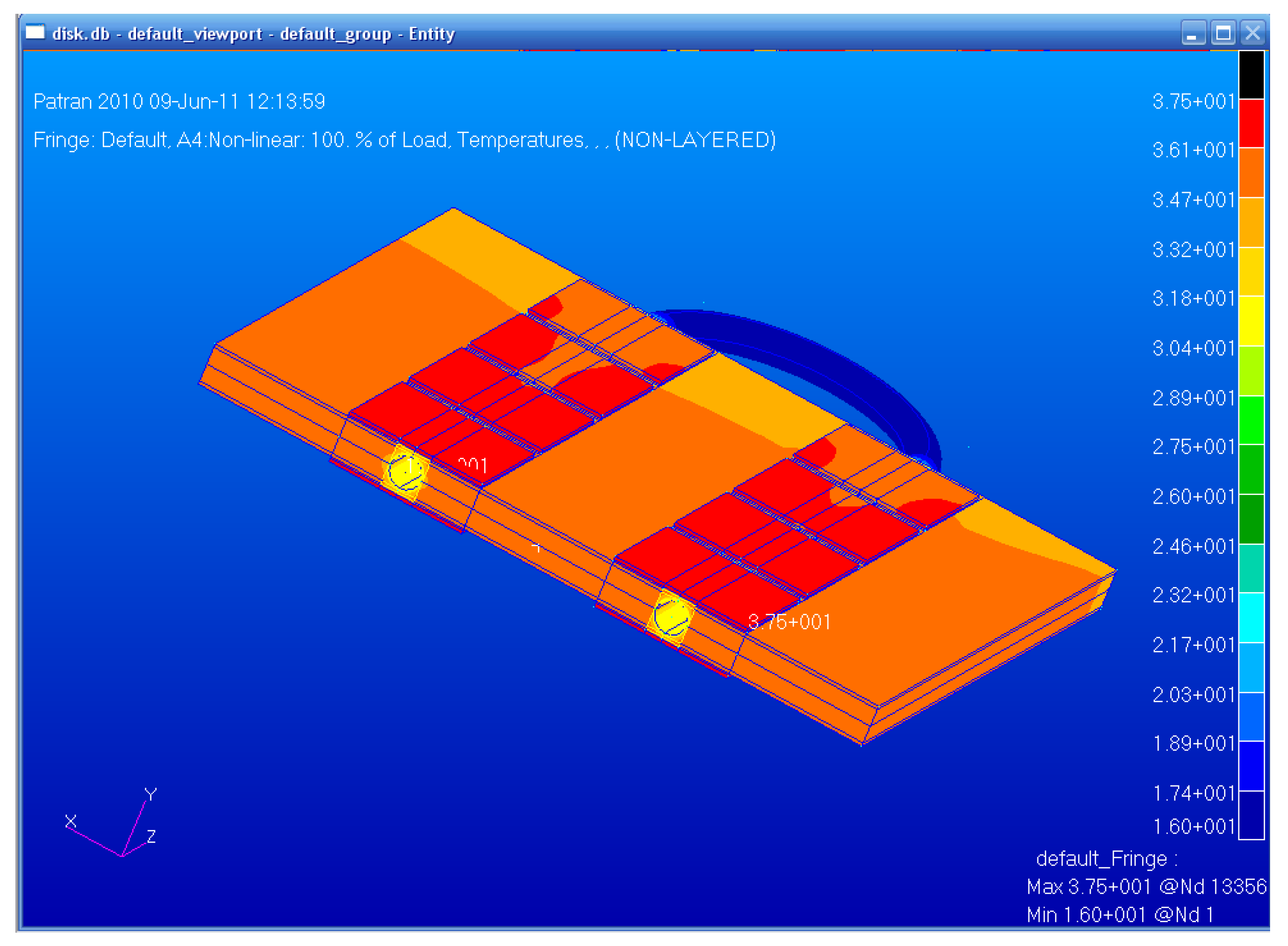
In the strip disk part the situation is more complicated because of a higher density of the readout electronics. Here the achieved temperature of the readout electronics would be 37.5 ∘C which is slightly above the required 35 ∘C. To solve this problem without changing the cooling concept would require to either reduce the power consumption of the electronics or double the number of cooling pipes which would result in a chip temperature of 28 ∘C. While a doubling of the cooling pipes would significantly increase the material budget in this part of the detector the first solution would be more desirable but it is not clear if this goal can be reached.
5.6.3 Cooling Plant
The cooling plant will be placed in a reserved and dedicated area at about m far from the MVD final position. In this area the inlet pump to feed all the cooling circuits, the tank for the water kept in depression mode by vacuum pump, the heat exchanger connected to a chiller, the water cleaning apparatus, the control unit and the manifolds for the supply and the return lines of the cooling circuits, each equipped with valves, regulators and sensors, will be located. A simple scheme of the hydraulic circuit is shown in figure 5.42.
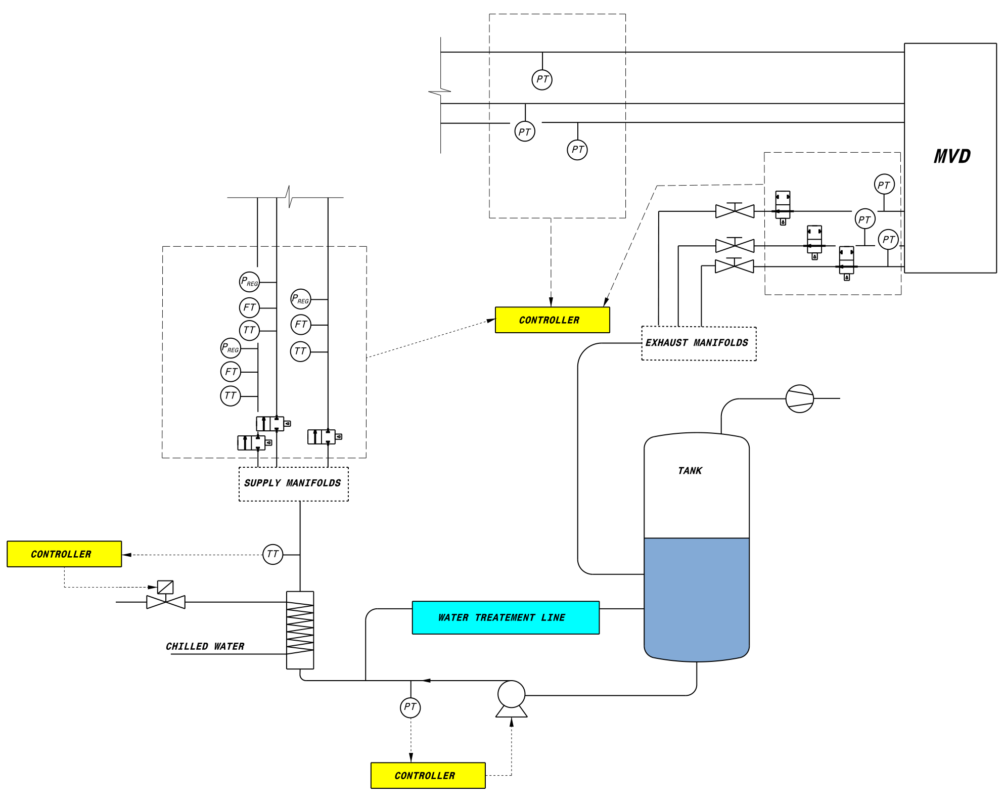
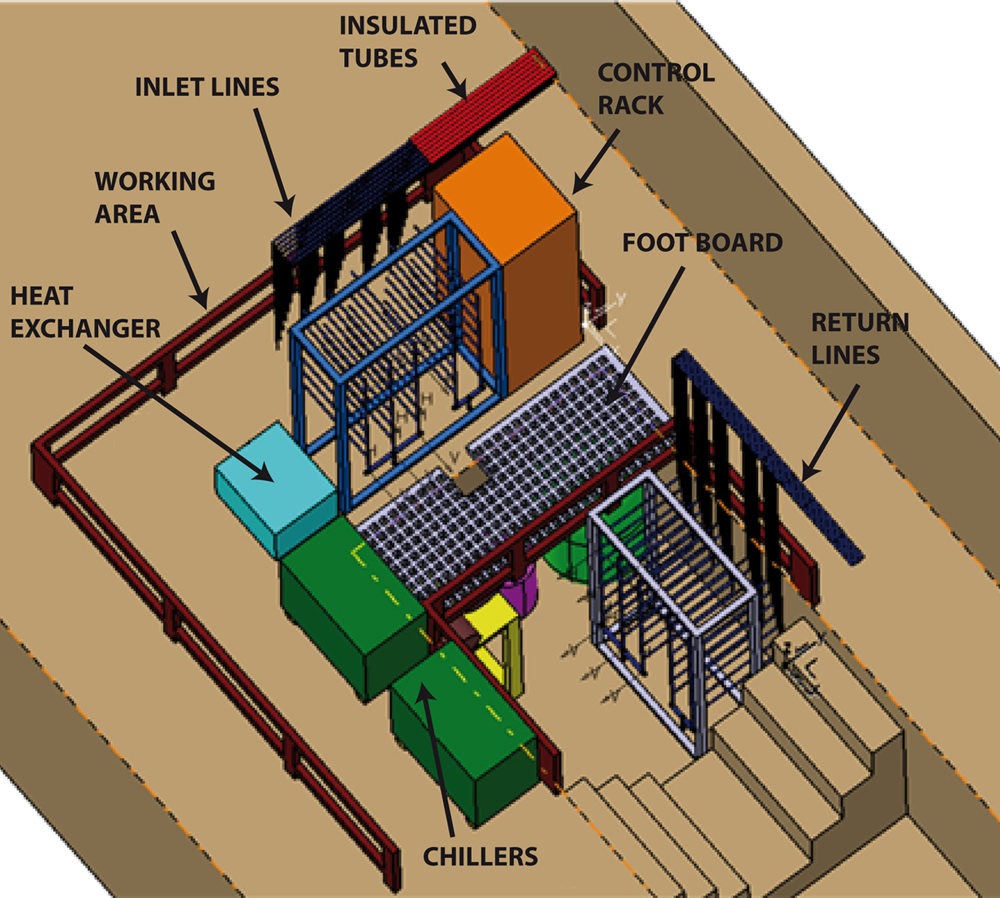
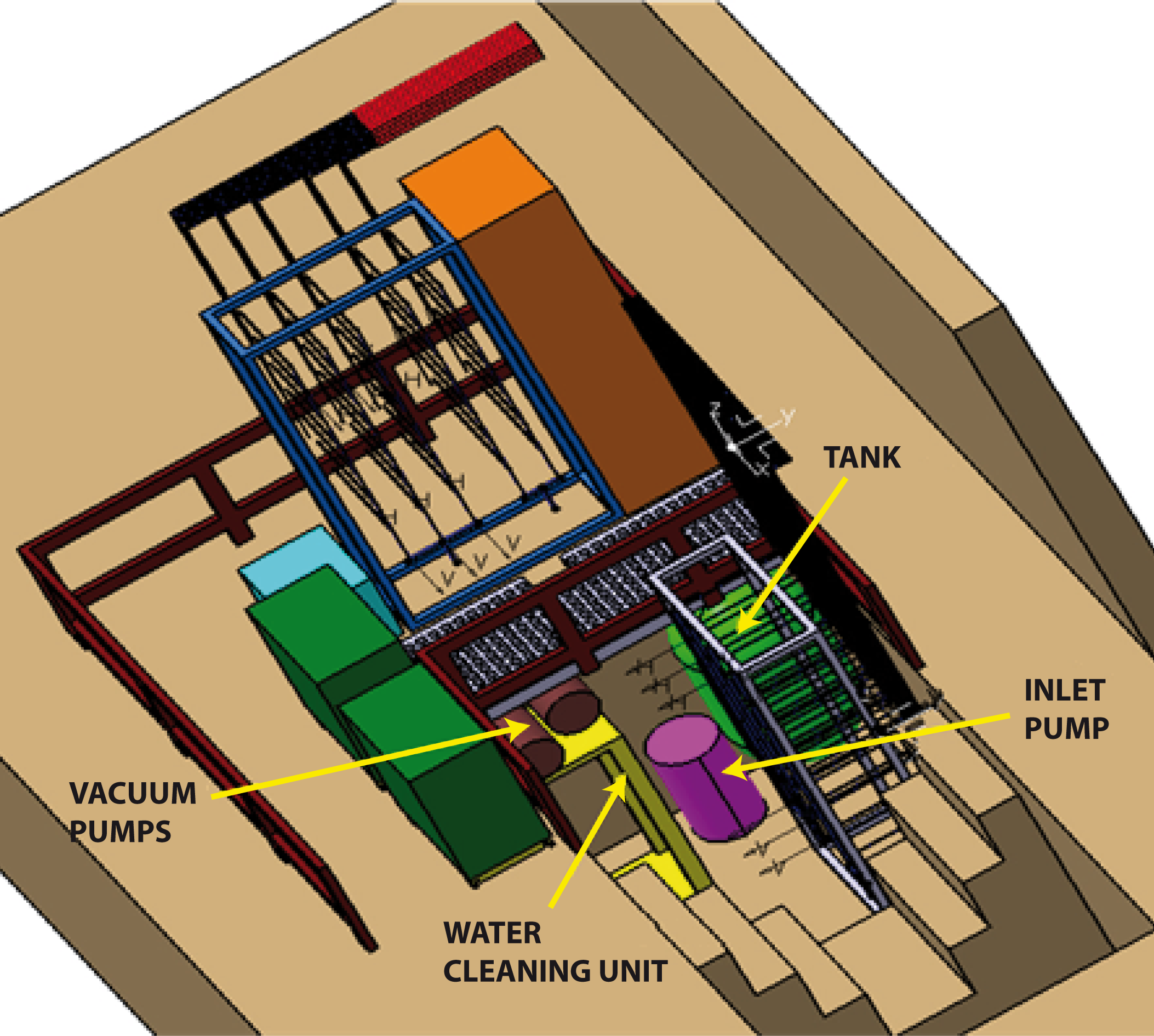
For fault-tolerance reasons, the pixel cooling system is segmented in different cooling loops, 9 for the barrels, and 12 for the disks, respectively. In the barrel, 3 cooling circuits are foreseen for layer 1 and 6 for layer 2. In the disks, 4 cooling circuits are for the two small disks and 8 cooling circuits for the bigger ones. The total number of cooling circuits for the pixel part is 21. For the strip part there are 32 cooling circuits, 24 for the barrel part and 8 for the strip part. The most important requirement for the hydraulic system is that it works at sub-atmospheric pressure, all along the MVD, ensuring a leak-less system. To achieve the sub-atmospheric pressure inside the detectors, the pressure drops along the detectors and the return lines are limited.
Pressure sensors on the supply lines, at the entrance of the MVD, ensure to operate in depression mode, while flow meters and pressure regulators on each cooling circuit, positioned at the cooling plant, guarantee the pressure stability and the nominal operating conditions.
All the metallic tubes and the wet parts of all the accessories (sensors, valves, flow meters, filters and fitting) will be in stainless steel AISI 316. The flexible tubes will be in polyurethane.
The water purity required for corrosion concerns of thin cooling pipes, will be obtained with a cleaning treatment chain which consists of deioniser, micro porous membrane to remove the dissolved O2 and sterilisation UV lamp [re:coolRef_1].
In figure 5.43 preliminary drafts of the cooling plant are shown.
5.7 DCS
For a reliable and safe detector operation the monitoring of operating parameters is crucial. Therefore a Detector Control System (DCS) will be deployed to permanently monitor parameter of importance for the MVD. This data will be collected and provided to the shift crew while running the experiment. The occurrence of critical values outside predefined parameter ranges need to create an alert or even cause an interrupt so that measures can be taken to prevent disturbance in operation or even a damage to the detector. The data shall be archived in order to evaluate the detector performance over time and identify possible problems. The \pandaExperiment Control System (ECS) will be based on EPICS111Experimental Physics and Industrial Control System. It allows to collect, display, and archive sensor readings from various devices. The following parameters should be kept under surveillance:
-
•
voltage and current of the \frontendelectronic
-
•
voltage and leakage current of the sensors
-
•
temperature of electronic and coolant
-
•
coolant flow
-
•
temperature and humidity in the detector volume
The supply voltages and the current consumptions of the \frontendelectronics will be measured at the power supplies and the voltage regulators close to the detector.
For the silicon sensors the depletion voltage and the leakage current have to be supervised. They give an indication of the condition of the sensors and can be used to check the radiation damage the sensors have taken. Here a measurement at the power supplies will be performed.
The sensors and, to a lesser extend, the electronics are very sensitive to the operation temperature. A close surveillance of the temperature and the cooling system are therefore very important for a safe and stable operation of the MVD.
Thus each pixel module and each strip super module will be equipped with an NTC thermistor to measure the temperature on the module. The readout cables of the resistors are routed along with the signal bus to the patch panel. Here the resistivity is measured and the data is fed into the DCS system.
The cooling system is monitored via temperature and pressure sensors on each cooling pipe and the correct temperature of the water in each pipe can be kept by a dedicated heater. In addition the overall temperature and humidity in the MVD and the temperature of the off-detector electronics will be measured and controlled.
References
Chapter 6 Monte-Carlo Simulations and Performance
A full simulation of the \pandadetector components and their answer to the passage of particles has been developed within the PandaRoot framework [pandaroot:chep08]. The simulations for the \Mvdare implemented within that framework. The same reconstruction and analysis algorithms and infrastructure will work on the simulation output as well as on real data.
This chapter will give an overview of the framework, the MVD detector and reconstruction code, as well as the results of performance studies.
6.1 Software Framework Layout
The software framework is the collection of software and tools for the description of the detectors and the simulation of physics reactions. The layout is organized such as to allow the re-use of well known programs and tools, common to particle and nuclear physics simulations. One basic concept of the framework is its modularity, the possibility to switch algorithms and procedures at mostly any point in the chain of processes. Hence a set of interfaces and data input/output is provided to connect all these tools properly.
In practice the frameworks organization features these levels:
-
•
External Packages containing the main bulk of software: Geant3 and Geant4 (Particle propagation through matter in Fortran [Geant3] and C++ [GEANT4]), VMC (Virtual Monte-Carlo [vmcweb2010], [Hrivnacova:2003yy]), ROOT (Plotting, fitting, graphics etc. [Brun1996]), Pythia [Sjostrand:2007gs] and auxiliary tools
-
•
FairRoot handling the framework, data I/O, interfaces, infrastructure
-
•
PandaRoot for detector simulations, tracking and reconstruction
To this framework, user processes are added as detector class implementations for the transport model and as tasks, which steer the processing at any stage. The availability of online parameters is provided with the runtime database (RTDB) and data are stored in a ROOT file, using ROOTs objects handling with chains, trees and branches. Using VMC, together with the geometry description in ROOT format, it is possible to switch between different transport engines. This enables an easy way to compare the outputs of different engines with each other and with real data in order to get a reliable description of the detectors behaviour.
A typical chain of processing is sketched in figure 6.1. It has the following stages:
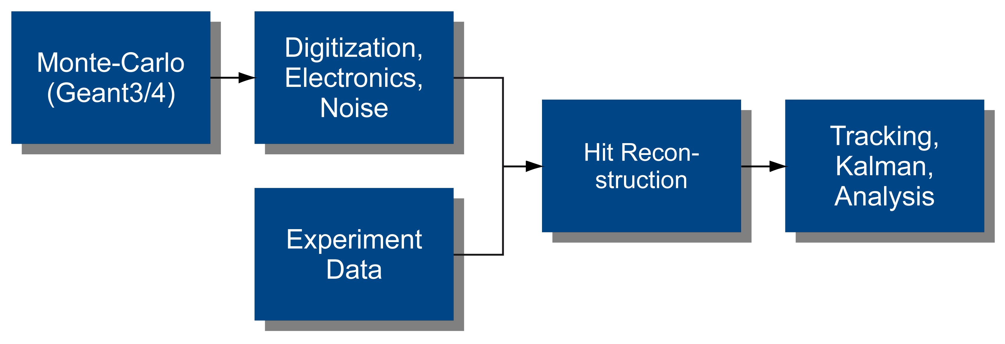
Event Generator: The event generator produces in each event a set of particles to be processed. Particles are defined by their four-momentum, charge, creation point and time. These properties are randomly distributed by the selected model, such as the technically important “particle gun”, single-channel generation with EvtGen [Evtgen] or the full description of antiproton-proton or antiproton-nucleus background reactions with DPM111Dual Parton Model [DPM] and UrQMD222UltraRelativistic Quantum molecular Dynamics model for \pbarN[UrQMD],[UrQMD2] respectively. Also Pythia and Pluto are available.
Transport Code (VMC): The particle transport through matter is usually simulated with one version of Geant. The Virtual Monte-Carlo interface (VMC) allows to switch between the different Geant flavors and allows to introduce other packages as well. Each sub-detector has its own geometry description (ROOT format) and the and the definition of the active elements in which the interaction of particles can occur according to different, selectable, physical processes (such as energy loss by ionization, showering or Cherenkov emission).
Digitization: All Monte-Carlo-Data are processed to model the detectors answer or to produce the effective answer of a readout chip. The digitized data formats out of the simulation must be the same as those obtained in a real implementation, such as a prototype detector or even the final setup.
Local Reconstruction: The digitized data are subject to a local reconstruction procedure which associates them to information with a physical meaning, like a 3D point (from \Mvd, GEM and central tracker), a total energy (from \Emc) or a Cherenkov angle (from \Dirc, \Rich).
Tracking: The tracking procedure in PandaRoot proceeds through two steps: track finding (pattern recognition and track prefits) and track fitting (Kalman filter). While the track finder algorithms are very different for each sub detector (or combinations of them), the fitting is done by means of the GENFIT package [Genfit2010], based on the kalman filter technique [R.E.Kalman1961], [Fruehwirth1987444], using GEANE ([GEANE1991], [A.Fontana2007] and [Lavezzi2007]) as propagation tool.
PID: Particle Identification is performed globally, taking information from all detectors into account. Each detector provides probability density functions (p.d.f.) for each particle kind, merged together to provide a global identification probability using Bayes theorem. In addition, different multi-variate algorithms are available, such as a KNN333K Nearest Neighbors Classifier Classifier or a Neural Network approach. The tuning of these algorithms still is ongoing.
Physics Analysis: The analysis tools have to deal with a collection of information based on four-momenta, positions and the identity of the reconstructed particles in a unified way. Particle combination, selection mechanisms and manipulation tools (like boosting between lab and center of mass frame) are provided. Furthermore a set of fitters is available to fit the four momenta and positions of particles (e.g. from a decay) under different types of constraints.
6.2 Detector Model of the MVD
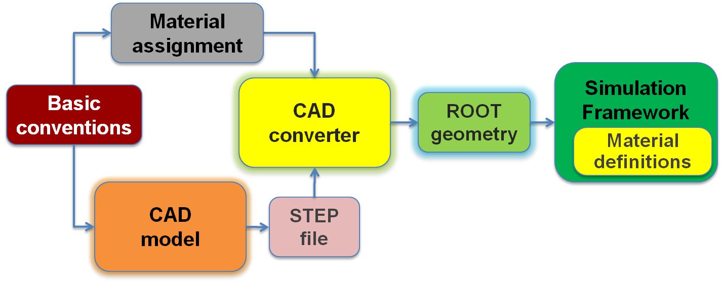
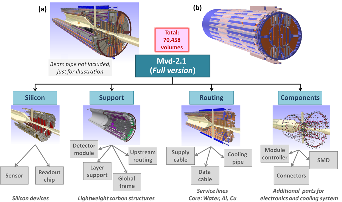
Along with the hardware developments a very detailed CAD model of the MVD has been accomplished, which delivers a very comprehensive and accurate detector description [NIM-MvdCadModel]. It is based on a design optimization between a good spatial coverage on one hand and the introduction of sufficient space needed for passive elements and the detector integration on the other. Thereby, a minimum material budget is achieved. The model includes active silicon detectors, connected readout electronics, local and global support structures, cables, a dedicated cooling system as well as the routing of all services. In addition, connectors and electronic components such as surface-mounted devices (SMD) are introduced. In total this comprehensive detector description contains approximately 70,500 individual volumes.
A converter [CAD-converter] has been developed to transform the CAD model into a ROOT geometry suited for simulations within the PandaRoot framework. It uses a common output format of CAD software (STEP format [STEP]) as input data. Besides the proper definition of the entire CAD in a ROOT geometry, material properties, i.e. the density and the radiation length, are given explicitly for each of the components. Therefore, basic conventions have been fixed, which allow for an unambiguous and automated allocation of each single volume [PANDAnoteCAD]. A schematic illustration of the procedure described is given in figure 6.2.
The main structure of the available detector geometry is shown in figure 6.3. At the top, an illustration of the model before and after the conversion is shown. Basically there are four functional parts, which are introduced as independent objects. The silicon part contains all silicon detectors, i.e. the pixel and the strip sensors, along with all associated readout chips. The second group is formed by the support structures of the detector. It includes the local support for detector modules and the individual detector layers as well as the global frame for the overall detector integration of the MVD. Moreover, a schematical support structure needed for the routing of services in upstream direction is added. All support components are defined as lightweight carbon composites of different effective density and radiation length.
The entire model of the routing part scales with the number of readout channels and is based on low-mass cables and the overall cooling concept outlined in chapter 5.4 and 5.6, respectively. Different cable types are introduced for the high voltage supply of the sensors, the power supply of the readout electronics as well the data transmission and slow control of the readout electronics. All cables are split into a conductive core and an insulation layer. The cooling lines consist of a water core and a casing material, which is defined either as steel or PVC. The barrel layer services are guided straightforward in upstream direction following the shape of the target pipe. The disk services are lead out to the top from where they are further extended in upstream direction. The concept for the pixel disks is more complex because the inner layers are inserted inside the barrel part. Therefore, they must be routed at first in forward direction until a position from where they can be brought to outer radii. While for all other parts a circular arrangement is chosen, the routing of the pixel disks is performed at the top and bottom.
The last part of the MVD model includes additional components of the electronics and cooling system. In the latter case these are given by connectors needed for the intersection from steel pipes used on the detector modules to flexible pipes at the outer part of the cooling circuits. The electronics part includes capacitors and SMD components, i.e. condensators and resistors, in order to deliver a complete description of fully equipped detector modules.
6.3 Silicon Detector Software
A software package for strip and pixel silicon sensors, called Silicon Detector Software (SDS), has been developed to reproduce both the \Mvdand the Luminosity monitor in the PandaRoot framework.
6.3.1 Monte-Carlo Particle Transport
Particles produced in the event generation phase are transported through the detector geometry and the magnetic field by the selected Monte-Carlo engine. When a particle crosses an active volume, a Monte-Carlo object is stored, containing the entry and exit coordinates, the total energy loss inside the volume, as well as the exact time the interaction in the detector occurs..
Passive detector components, e.g. holding structures, contribute with their material budget to scattering, energy loss, secondary particle production (delta-electrons) etc.
6.3.2 Digitization
Digitization is the emulation of the detector answer before using reconstruction algorithms. The entry and exit coordinates and the charge information are used to determine which pixels or strips fired. The output data is the same format like the real data will have. Each fired strip or pixel is called a “digi”, identifying the strip/pixel itself as well as the involved \frontendchip and the sensor. Furthermore the measured charge and the determined time stamp are stored. The digitization is a process in two stages, geometric and electronic digitization, described below.
Geometric Digitization
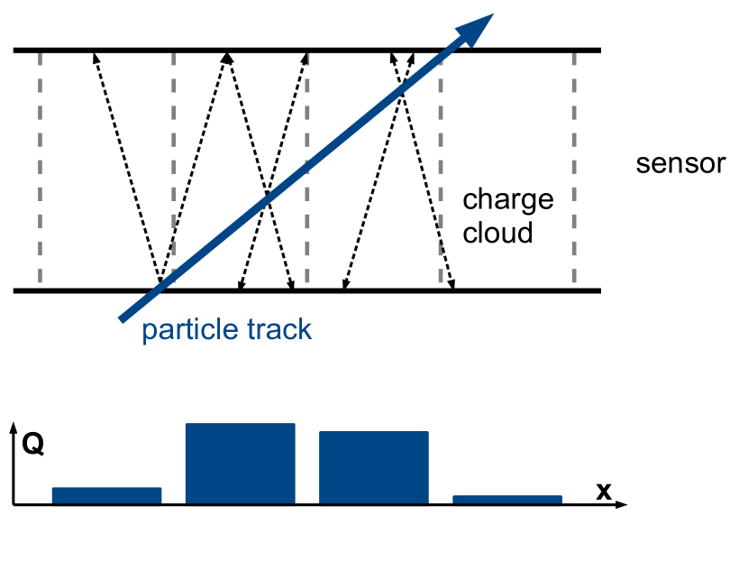
Geometrically one can project the particle path through the sensor to its surface. As the path crosses the readout structure the discretization into pixels or strips is done. The charge collected in each of the channels is calculated by a gaussian cloud distribution around the path (illustrated in figure 6.4). The charge for one strip is given by
| (6.1) |
and the charge in one pixel is
| (6.2) |
Q being the total number of electrons produced by the particle, and (y respectively) the entry and exit coordinates of its track and being:
| (6.3) |
The width of this cloud is a parameter which is assumed to be in the order of 8 m.
Electronic Digitization
Charge from the sensors is measured in the \frontendelectronics with the Time-over-Threshold method (ToT) (See also section 3.3.3). The charge is integrated in a charge sensitive amplifier (CSA), at the same time the capacitor of the CSA is discharged by a constant current source. The output of the CSA then is compared with a threshold voltage. The time the amplifier output is above this threshold is proportional to the deposited charge.

The SDS package provides the possibility to include different models for the ToT calculation.
The simplest model for the \frontendchip behavior is the triangular one (See figure 6.5). It assumes a linear rising and falling of the signal with a constant peaking time: The characteristic parameters are the peaking time, the constant discharge current and the discriminator threshold.
For the event building it is necessary to mark every digi with precise time information, the Time Stamp. In reality the Time Stamp is set by the \frontendelectronics when the rising signal crosses the threshold voltage. Due to the not negligible rising time of the preamplifier this time is not the same instant the particle hits the sensor. This delay between the physical hit and the recognition by the electronics is called Time Walk (figure 6.5).
The simulated Time Stamp of a digi is the sum of the Event Time (MC information), the flight time of the particle till it hits the frontside of the sensor and the Time Walk of the Signal.
6.3.3 Noise Emulation
Electronic noise has the character of a gaussian distribution, centered around the baseline with the width of . The noise baseline is set as the nominal zero in the simulations. To deal with the electronics noise each collected charge in a pixel and strip channel is redistributed by the noise gaussian with electrons for pixel sensors and electrons for the strip sensors, as the hardware measurements show (see sections 3.3 and 4.2). A threshold cut is applied to suppress too low charge entries being set to . The gaussian tail over the threshold will produce hits by the noise statistics (see figure 6.6). This is taken into account by adding randomly selected channels. The number of noise hits is calculated by a poissonian random distribution with its mean value being
| (6.4) |
while is the time interval from the previous event and the bus readout frequency and being the complementary error function.
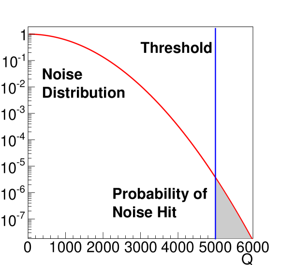
6.3.4 Local Reconstruction
Digitized data are reconstructed by finding clusters and forming hits at the clusters centeroid, using the charge measurements to improve the accuracy. Furthermore the time of the particle passage is reconstructed by the time walk correction.
Cluster Finding
Cluster finding means to collect all digis belonging to one track passing through the sensor. This is done iteratively by taking all signaling channels around one digi wthin a given tolerance of channels. A minimum charge sum of a clusters digis can be required to reject ghost hits produced by noise only.
Hit Reconstruction
Having a cluster of digis, calculating the centeroid finds several approaches [V.Radeka1980].
Simply taking the central position of the channel with the highest charge yield in a cluster defines the binary centeroid. Its uncertainty is . This method is the only option to calculate coordinates with only one entry per cluster.
A better resolution for clusters with two or more digis is given by the center of gravity, which uses the digis charge measurements as weight. The average position is calculated by
| (6.5) |
This approach mirrors the geometric digitization procedure in the sense of isotropy in the readout structures and the lack of magnetic field effects. The precision is smaller than , which will be shown in section 6.7.
To get a precise 3D information with the strip sensors, top and bottom side hits have to be correlated. This produces ambiguities when at least one of the sides of a sensor has more then one cluster. Such a situation is created by multiple tracks hitting a sensor in one event or in case of hits generated by electronic noise. Because the charge carriers arriving at either side correspond to pairs produced by the same particle, a correlation in the measured charge (in form of a cut in the charge difference ) can reduce the number of ambiguities.
Time Walk Correction
To improve the time resolution of the TimeStamp, a correction of the TimeWalk effect can be applied. Based on a ToT conversion model the TimeWalk can be calculated from the ToT value and subtracted from the TimeStamp.
For the triangular ToT model the TimeWalk is given by:
| (6.6) |
6.4 Tracking and Vertexing
The tracking procedure in PandaRoot proceeds through three steps. First, local pattern recognition algorithms find tracklets in different subdetectors. Afterwards a global track finding and tracklet merging is performed. The global tracks are then globally fitted.
6.4.1 \MvdTracklet Finding and Fitting
The track finding and pre-fitting for the hit points inside the MVD is based on a fast circle fit using the x-y-coordinate of a hit point and a second linear fit of the arc length of a tracklet on the fitted circle and the z-coordinate. For a computational fast circle fitting a translation of the hit points to a Riemann surface is performed. Here a plane is fitted to the track points. The parameters of the plane can be than back calculated to the circle parameters mid point and radius. A detailed description of the algorithm can be found in [Fruehwirth2002366].
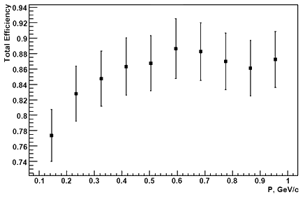
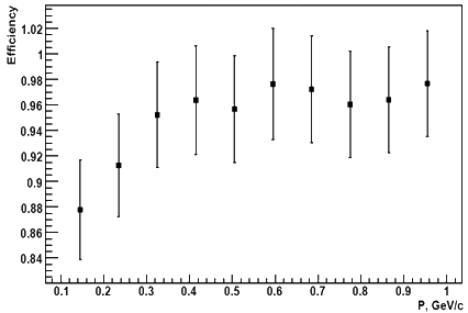
The performance of the track finder is shown in the following figures. Six charged tracks per event with a random angular distribution and random momentum between 0.1 \gevcand 1 \gevchave been simulated. In the first diagram (figure 6.7) the number of correctly found tracks divided by the number of all simulated tracks is plotted against the momentum of a single track. The error bars indicate the variation of the track efficiency for different theta angles. For tracks with very low momenta of about 100 \mevcthe finding efficiency is about 77% which rises up to 88% for tracks above 600 \mevc. The increase of track finding efficiency with rising momentum can be explained by the dominance of multiple scattering for low momentum tracks. The low overall track finding performance inside the MVD is coming from the low number of hit points per track. In the second diagram (figure 6.8) the efficiency was calculated for all tracks with at least four hit points in the MVD, which are required for a successful track finding.
If one calculates the tracking efficiency only for those tracks with at least four track points it starts with 88% at 100 \mevcand rises up to 97% for tracks above 400 \mevcThe error bars are exceeding 100% due to tracks originating from the primary vertex with only three hit points. They can be found by the Riemann-Track-Finder as well but they are not used for the efficiency evaluation.
To improve the overall track finding efficiency a combination of the MVD hit points with those of the central tracker is necessary, as explained in subsection 6.4.2.
6.4.2 Track Finding
The global track finding operates in a sequence, each step combining several detection systems. First tracklets from the STT pattern recognition are merged with the \Mvdtracklets and unmatched \Mvdhits. Second, any unmatched \Mvdtracklets are merged with remaining STT hits. Then, all remaining \Mvdand STT hits are checked for forming new track candidates. Finally, the GEM disk hits are matched to the existing track candidates. Each step features an update of the track description parameters, as well as a more stringent condition to clean the candidates of spurious solutions. A detailed description can be found in the STT technical design report [SttTdr].
6.4.3 Track Fitting
Track fitting in \Pandais performed globally using all tracking devices. It employs the Kalman Filter ([R.E.Kalman1961], [Fruehwirth1987444]) technique using the GENFIT package [Genfit2010]. Particle transport is done with the GEANE package ([GEANE1991], [A.Fontana2007] and [Lavezzi2007]), which backtracks charged particles in a magnetic field, taking care of energy loss and scattering in materials. For each track a momentum resolution of and is achieved [SttTdr]. By default all tracks are propagated to the point of closest approach to the z axis to form particle candidates.
6.4.4 Vertex Finding Algorithms
Finding the common starting point (vertex) of several tracks is the central goal of the \Mvd. There are several approaches under development. For primary vertices and short-lived particle decays, all tracks are treated purely as helices, because scattering and energy loss are negligible inside the beam pipe vacuum.
POCA Finder
A first approach is to find the point of closest approach (POCA) of two tracks, which is done analytically. Both helices are projected to the x-y-plane, assuming a constant magnetic field in z direction, forming circular trajectories. The intersection, or minimal distance, of the two circles defines the desired region. This is not the POCA in a full 3D treatment, but produces a good approximation for tracks originating from the same vertex. The calculated distance between the tracks gives a measure on how well this assumption holds.
Having more than two tracks combined, the idea is to average the POCAs of each combination of two tracks, weighted by the inverse of the tracks distances . For n tracks one gets the vertex :
| (6.7) |
To evaluate the ”goodness” of the retrieved vertex the inverse of the weights sum is used:
| (6.8) |
This method does not take the tracks covariances and error estimates into account, hence is not able to estimate the vertex covariance and error. However, in order to find a seed value for a fitter or to reject outlying tracks from bad combinations this ansatz is fast and useful.
Linearised Vertex Fitter
In this approach [Billoir:1992yq] the tracks are locally parametrized and their propagation close to the expansion point444Point chosen where to do the parameterization and linearization procedure. It is the Origin for vertices close to the interaction point is linearized. The fit’s basic idea is to reduce the dimensions of the matrices to be inverted. For tracks one gets -matrices (5 being the number of parameter necessary to describe a helix, while two of them, the polar angle and the trajectory curvature, remain fixed) to be inverted instead of one 55-matrix in the general case. This improves the calculation speed of the fitter but lacks precision. The procedure is slightly sensitive to the choice of the expansion point, thus a good estimate on the vertex position is required.
Because of the imposed linearisations the calculation of the track parameters and covariances feature mainly sums over the tracks. Hence it is quite easy and fast to add or subtract tracks from the set without repeating the full calculations. This procedure is very useful to reject outlying tracks or to form mother particle candidates “on the fly” by vertex constraint only.
The procedure may be separated into two parts, one being a fast vertex fitter and the other the full fitter, which also fits the particles four-momenta. The calculation of the covariance matrices and the gives the estimate of the fit quality.
Kinematic Vertex Fitter
A vertex constrained kinematic fitter is available. It is based on the Paul Avery papers (e.g. [avery4] and [avery5]) and fits the whole set of momenta and the vertex position. It employs the inversion of the whole 55-matrix for the 5 helix parameters of the tracks. The fit quality is estimated by the value and the covariance matrices.
6.5 PID Algorithm for the \Mvd
The passage of a particle through matter is characterised by a deceleration due to the scattering with the quasi-free electrons therein. The energy loss information can contribute to the global particle identification (PID), especially in the low momentum region (below a MIP), where the Bethe-Bloch distribution is steeper depending on the particle mass. Because the energy loss process has a statistical nature, it’s necessary to reproduce the behavior of a probability density function (p.d.f), of the energy loss, that will depend on the particle momentum and on the measurement uncertainty. Different statistical approaches have been investigated in order to obtain a robust PID algorithm.
6.5.1 Energy Loss Information
The energy loss information of different particle species have been studied and parametrised. The interaction of various particles has been simulated within PandaRoot using Geant4 and the reconstruction tools available in the framework. In order to take the uncertainty of the detector and of the full track fit into account, the reconstructed tracks have been used. The total energy loss of a track is considered, which corresponds to the energy loss through few hundreds m of silicon, because the number of contributing hits will be at maximum 6 in the forward part and 4 in the barrel part. The energy loss distribution of the reconstructed tracks for different particles is shown in figure 6.9.
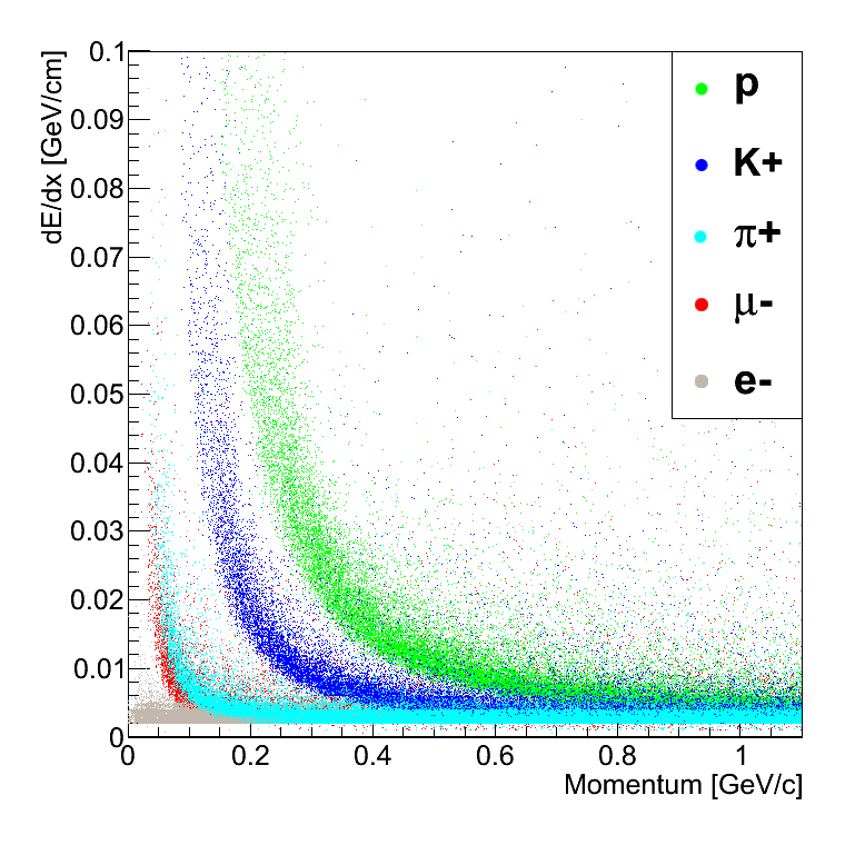
6.5.2 Statistical Approach for the Energy Loss Parametrisation
Different statistical approaches have been studied to assign a estimator to each track.
The arithmetic mean value of the energy loss
of course is not a good
estimator due to the long tail of the energy loss distribution. Several estimators have been compared,
applying different algorithms
to the single-particle tracks. To estimate the quality of the different estimators a comparison in
terms of standard deviation and of
efficiency and purity of the samples, selected by different algorithms, has been performed.
Each particle species has been simulated at seven different momenta from 400 \mevcup to 1 \gevcin
step of 100 \mevc,
then the energy loss of the reconstructed tracks has been studied.
The particle energy lost in each layer is approximated by the quantity
where
is the energy lost in each sensor (measured by the integrated
charge of a “cluster”, i.e. a set of neighbouring pixels or strips), D is the active sensor
thickness, and is the angle between the track direction and the axis normal to the sensor surface.
The distribution of the track energy loss has been fitted with a Gaussian or with a Landau function in
order to find the mean
value, or the most probable value (mpv), and the corresponding sigma for the different particle species
and for different momenta.

Mpv of a Landau Distribution
A unique specific energy loss
value along the whole trajectory is estimated, because the loss of energy through each layer is negligible with respect to the considered momenta. Such a value is calculated as
| (6.9) |
where
n is the number of track hits in the MVD, is the energy
lost by the particle in each layer, and is the crossed thickness.
A Landau distribution has been used to fit the total reconstructed energy loss of each track. The most probable values and the
related sigmas
have been used for the parametrisation.
Median
The median of a distribution is calculated by arranging all the of the track on the different detector planes from the lowest to
the highest value and picking out the middle one (or the mean of the two middle value in case of even observations). The mean value and the sigma
of the Gaussian distribution obtained from the different tracks is used as reference value of the energy lost by that particle at a given
momentum.
Truncated Mean
The truncated mean method discards the highest value in a fixed fraction of the total number of observations,
calculating the mean
of the remainder values. In this study 20% of
the hits are discarded. This cut is applied only if a track has more then 3 hits.
Generalised Mean
The “generalised mean” of grade of a variable is defined as:
| (6.10) |
In this case the grade = -2 [CMSnote] has been used.
The separation power (SP, [SepPow]) has been calculated as:
| (6.11) |
where is the mean value (or the mpv) of the energy lost by a particle at a certain momentum, p1 and p2 are two particle species to be separated and is the standard deviation of the distribution. The separation power p/K, p/ and K/ for the different algorithms is shown in figure 6.10. As expected the separation power decreases with the increasing momentum.
Even if the Landau distribution shows a better separation power (because of the smaller sigma of the Landau distribution, at least by a factor 2), it is not the most suitable estimator because of the long tail, which introduces a significant contamination.
In order to build a probability density function, the trend of the mean (or MPV) values and of the sigma as a function of the momentum have been fitted by the following function:
| (6.12) |
where a, b and c are the parameters of the fit. As an example the parametrisation of the mean value of the median as a function of the momentum is shown in figure 6.11.
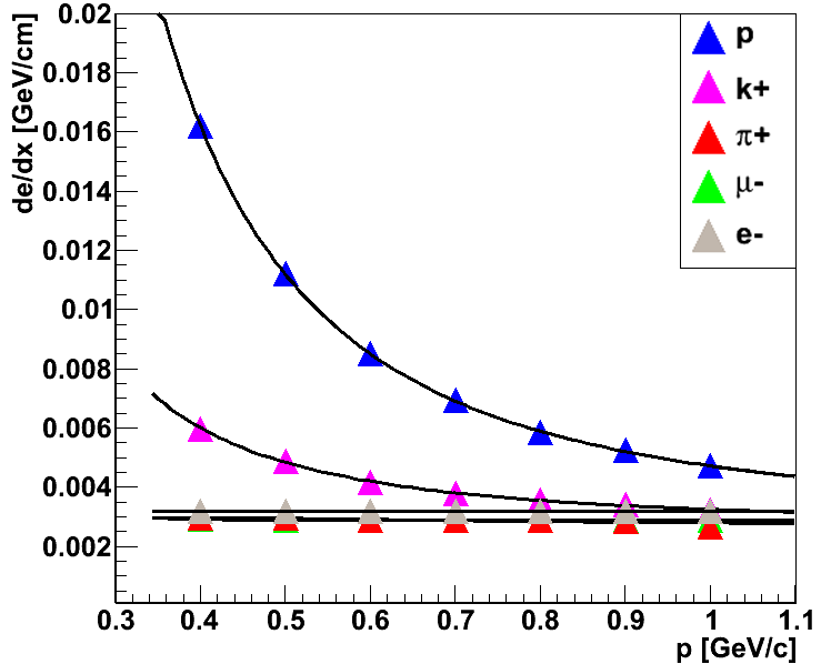
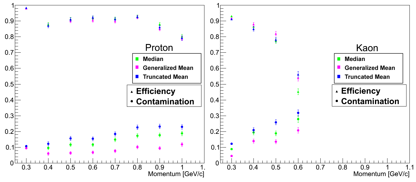
In this way, the momentum and the energy loss of a given reconstructed track are used to
build the probability density function and to extract the probability to belong to a certain particle species.
The efficiency and the contamination of the different algorithms has
been plotted as a function of the momentum for the proton and kaon hypothesis, as shown in figure 6.12,
using a probability threshold of 90% (i.e. the particle hyphotesis should have a
probability bigger than 90% to belong to a certain particle species).
The efficiency of proton identification is almost constant around 90%
and the contamination in the worst case (at larger momenta), is smaller than 30%.
The efficiency of kaon identification is more dependent on the momentum,
but it is larger than 80%, at least up to 500 \mevc. The
contamination is higher than in the case of proton, by a factor of 2 at 600 \mevc. The comparison of
the three algorithms shows that the efficiency is almost the same in
the three cases, while the contamination is smaller for the
generalised mean.
Other particle species are not taken into account because, as shown in figure 6.9, the signals of
pions, muons and electrons in the MVD are too overlapped to deliver a good identification
efficiency.
The MVD can contribute to the global PID decision up to a momentum of
500 \mevcfor kaons and up to 1 \gevcfor protons.
6.6 General Simulation Studies
6.6.1 Radiation Damage
Most important for the damage of the silicon sensors is the non-ionising energy loss which causes damages in the lattice structure of the semiconductor material which influences the collection efficiency and the leakage current of the sensor. The damage caused by a particle strongly depends on the particle type and its momentum. To compare the damage caused by different particles one can define a hardening factor which scales the different particle types to the damage caused by the flux of 1 \mevneutrons according to the NIEL hypotheses [Gunnar200330]. This scaling factor can be seen in figure 6.13 for various particle types.
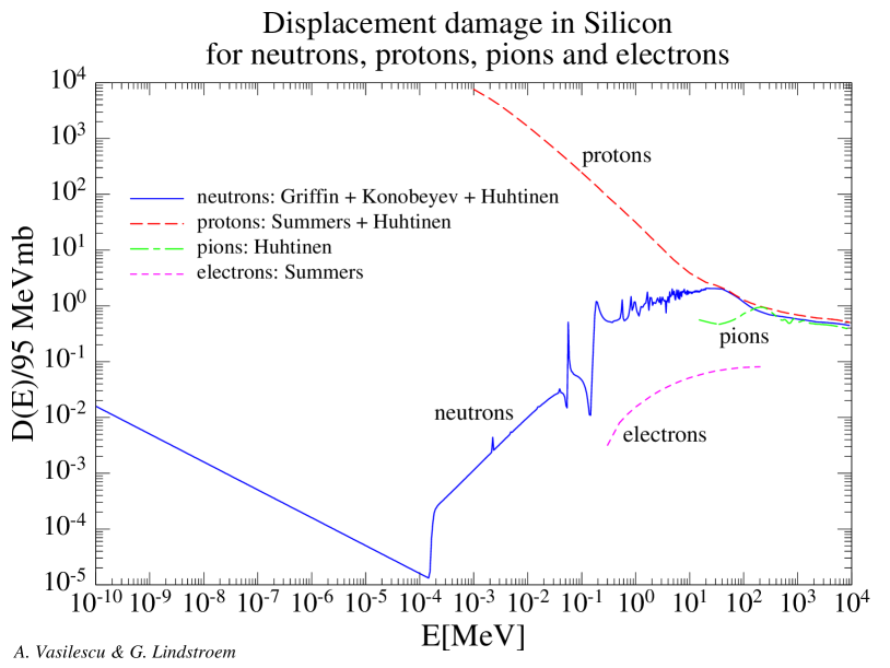
The simulation of the radiation damage was performed with the PandaRoot framework. Depending on the target material, two different event generators have been used: DPM111Including elastic Coulomb scattering with a cut off below a scattering angle of 0.17∘ for hydrogen targets and UrQMDSmm for nuclear targets. The generated particles then were propagated through the full \Pandadetector using Geant4 to include also backscattered particles from detectors further outside of \Panda. The neutron equivalent flux of particles then was determined by weighting each intersection of a particle with a silicon sensor with the momentum and particle type dependent scaling factor. This simulation was done for different target materials and beam momenta from 2 \gevcup to 15 \gevc. For each setting more than antiproton-target interactions have been simulated on the pandaGRID.
With the simulated events no time information is given. Therefore it is necessary to estimate the interaction rate R for different target materials and beam momenta to come from a fluence for a number of events A to a fluence for one operation year with .
| (6.13) |
The cross section for hydrogen targets is given by the DPM generator, the values for nuclear targets was taken from [Lehrach06].
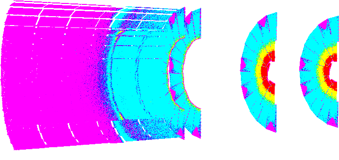
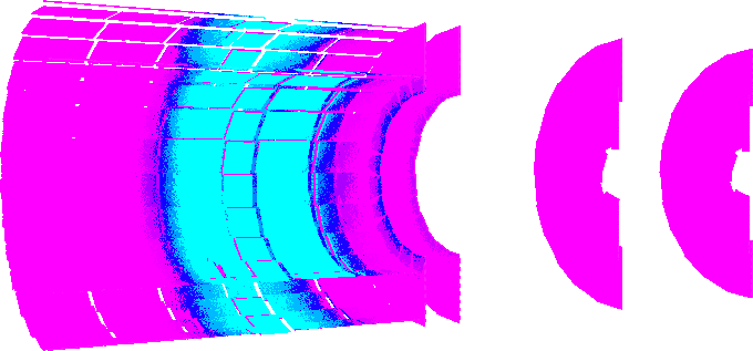


Figure 6.14 shows the different dose distributions for a light hydrogen target and a heavy xenon target for a beam momentum of 15 \gevc. The same diagrams can be seen for the pixel part in figure 6.15 for two beam momenta of 2 \gevcand 15 \gevcand for a hydrogen and a xenon target. The colour scale of the diagrams is different for the different setting and does not allow a comparison between the different drawings. For the light target the maximum radiation dose is seen for the inner parts of the forward disks while for the heavy target the distribution of the radiation dose is more isotropic with a maximum at the innermost barrel layers which are closest to the target.
The two histograms 6.16 show the overall dose distribution for the two different target materials for one year of \Pandaoperation. One can see a strong anisotropy of the distributions with few very hot regions and most areas with more than a magnitude less radiation damage than the maximum.
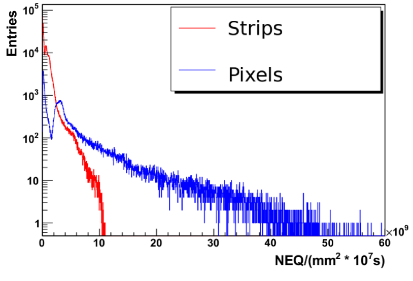
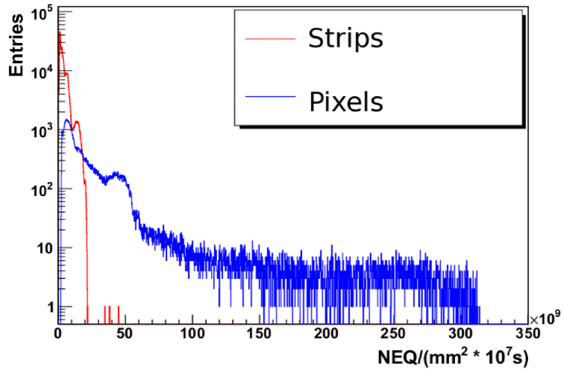
A summary of the radiation damage for one operation year for various target materials and beam momenta is shown in figure 6.17. This diagram shows the maximum radiation dose a square mm of sensor material sees in one operation year. For a hydrogen target it stays below \neueqwith only a slight increase with the beam momentum while for nuclear targets a strong momentum dependency can be seen with a maximum dose rate of \neueqfor a xenon target with 15 \gevcbeam momentum. A duty cycle of 50% was assumed for these estimates.
6.6.2 Detector Coverage
In order to achieve the required tracking performance, a high spatial coverage with a sufficient number of track points inside the MVD is needed. The implemented optimisation of the detector geometry aims at a minimum of four MVD hit points for central tracks at polar angles above 10∘. In this way an independent pre-fit of MVD tracklets can be performed by means of fast tracking algorithms (for details see 6.4.1). Moreover, for a precise vertex reconstruction the first hit point must be detected as close as possible to the origin of the track.
Extensive studies have been performed to evaluate the detector coverage obtained after the optimisation process. Therefore, a reduced model of the MVD was used, which only includes active sensor elements and no passive material. Due to the focus on mere geometrical aspects connected to the sensor dimensions and their arrangement in the individual layers, all pipes of the beam-target system were omitted thus minimising scattering effects. Material effects will be explicitly discussed in the next subsection 6.6.3.
In the presented coverage study, particles of fixed momentum were generated at the nominal interaction point and isotropically emitted over the polar angle, , and the azimuthal angle, . For the following particle propagation through the detector the magnetic field of the 2 T solenoid was switched on. Simulations were carried out in the PandaRoot framework [Group2007], which allows an interface to the Geant4 transport code [GEANT4]. Table 6.1 summarises all basic input parameters. The different setups were chosen in order to check a possible influence of the resulting bending radius on the effective detector coverage.
| MVD model | Only active elements |
|---|---|
| Magnetic field | T |
| Particle species | |
| Momentum / [\gevc] | 0.15, 0.5, 1.0, 1.5 |
| Particle distribution | Isotropic in and |
| Start vertex | |
| Number of events | 2 million / scan |
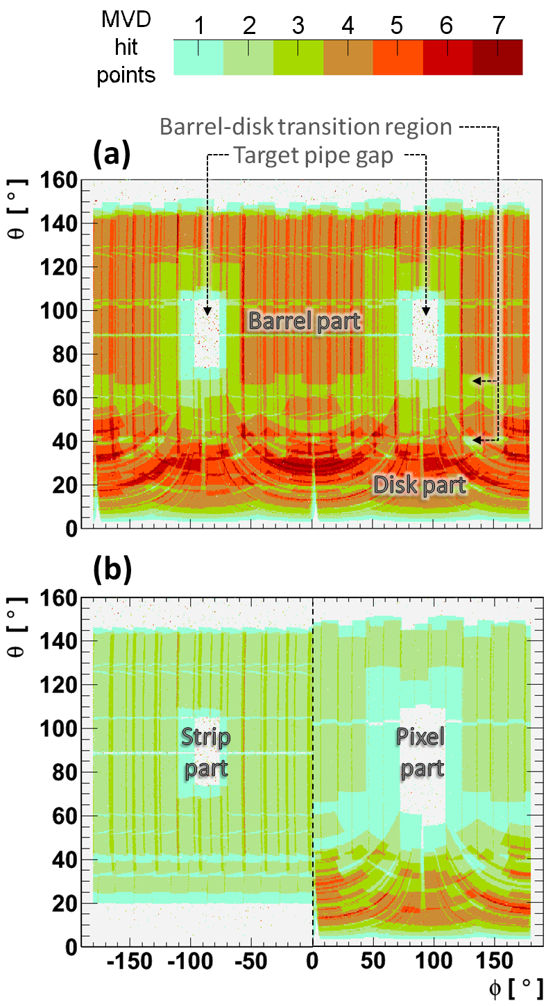
Due to the high statistical sample for each of the simulation runs, a fine-meshed mapping of the detector coverage becomes possible. A corresponding 2D diagram for one selected configuration is shown in figure 6.18 (a). In the chosen representation, the number of obtained MVD hit points per track is plotted colour-coded against its initial emission angles and . Contributions of the MVD can be observed in a polar angle interval from 3∘ to 150∘, which is in accordance with the basic detector layout (cf. figure 2.4). The envisaged design goal of at least four hit points is achieved in a large range of the solid angle. Regions with more than four hit points are related to the radial overlap of adjacent elements within one barrel layer and interleaves of different disk layers in the forward direction. The two gaps around reflect the keep-outs needed for the target pipe. Larger areas with a reduced number of hit points around the target pipe gaps and in the transition region from the barrel to the disk part are related to safety margins required for the overall detector integration. They reflect the adjustment to the crossing target pipe in each of the barrel layers and the fitting of the inner pixel disks inside the MVD barrel part, respectively. Smaller structures with a reduced number of hit points result from passive sensor edges.
In figure 6.18 (b) the overall hit distribution is split into the pixel and the strip part of the MVD. Due to the rotational symmetry of the MVD halves in , only the region between is shown for each of them. In both cases the barrel region between = 70∘ and = 140∘ is covered very homogeneously. Larger areas with a reduced number of hit points result from the adjustment to the crossing target pipe in the different barrel layers. A significant difference between the two main detector parts occurs in the forward region (). The six double-sided pixel disks deliver a more complex pattern compared to the homogeneous coverage of the two strip disks. Due to the approximation of disk layers with rectangular-shaped pixel sensors, the covered area in the - diagram corresponds to a circular arc shaped.
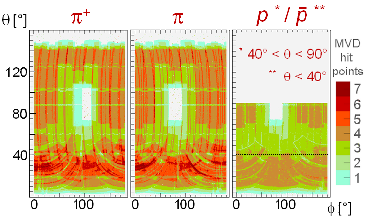
A comparison between different configurations is shown in figure 6.19. The opposed bending radius of charge conjugated particles with low momenta is reflected by the different curvatures of the overlaps in the barrel part. A comparison between different configurations is shown in figure 6.19. The opposed bending radius of charge conjugated particles with low momenta is reflected by the different curvatures of the overlaps in the barrel part. In case of low momentum nucleons strong attenuation effects can be observed. They are caused by interactions with the active silicon material during the particle propagation. Considering that in a realistic scenario all pipes of the beam-target system and the full material budget for the MVD must be included, it can be deduced that most of the slow nucleons with momenta below 200 \mevcget stuck in one of the MVD layers. In particular, this fact becomes relevant for elastically scattered recoil protons.
Quantitative results on the relative detector coverage in the maximum polar angle range from 3∘ to 150∘ are summarised in table 6.2. They are extracted from simulations with positively and negatively charged pions in a momentum range from 150 \mevcto 1.5 \gevc. The impact of opposed bending radii for the and the is very small, occurring deviations are dominated by systematic errors and statistical fluctuations of the simulation. Obtained values for a minimum of one and four hit points are in the order of 95% and 60% , respectively. The missing 5% in the overall acceptance is related to the target pipe gaps.
| Particle | Charge | Relative coverage within / [%] | ||||||
|---|---|---|---|---|---|---|---|---|
| momentum | conjugation | Number of MVD hit points | ||||||
| 1 | 2 | 3 | 4 | 5 | 6 | Total | ||
| 0.15 \gevc | 6.3 | 7.6 | 22.3 | 38.5 | 16.9 | 3.6 | 95.0 | |
| 4.5 | 9.0 | 21.0 | 38.4 | 17.1 | 3.4 | 93.2 | ||
| 0.5 \gevc | 6.1 | 6.4 | 23.0 | 39.7 | 16.9 | 3.8 | 94.9 | |
| 5.4 | 7.1 | 22.4 | 40.9 | 16.6 | 3.6 | 94.5 | ||
| 1.0 \gevc | 6.0 | 6.4 | 22.7 | 40.0 | 17.1 | 3.7 | 95.2 | |
| 5.6 | 6.9 | 22.4 | 40.8 | 16.6 | 3.8 | 95.0 | ||
| 1.5 \gevc | 6.0 | 6.4 | 22.6 | 40.2 | 17.1 | 3.8 | 95.2 | |
| 5.7 | 6.8 | 22.4 | 40.8 | 16.6 | 3.9 | 95.2 | ||
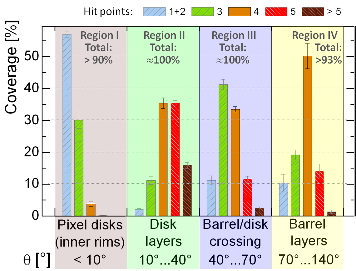
For a more precise evaluation in terms of physics performance, the total detector acceptance can be split into four main regions according to the basic design of the detector (cf. figure 2.4):
- Region I:
-
Polar angles between 3∘ and 10∘ representing the solid angle covered by the inner rims of the pixel disks,
- Region II:
-
Polar angles between 10∘ and 40∘ representing the solid angle covered by the forward disk layers,
- Region III:
-
Polar angles between 40∘ and 70∘ representing the solid angle covered by the strip barrel part, the outer pixel barrel layer and the innermost pixel disk delivering the fourth hit point,
- Region IV:
-
Polar angles between 70∘ and 140∘ representing the area covered by all four barrel layers.
The hit information in Region I contributes to the forward tracking systems, which basically use a straight line fit before and after the dipole. Therefore, one or two hit points from the MVD is already sufficient. The design goal of at least four hit points has been applied to the three remaining regions. They are connected to the central tracking part for which a helix fit must be performed. The most important part for many physics channels is given by Region II, which also includes the kinematic region of charged decay modes of the ground state \Dmesons. Compromises had to be done in Region III in order to obtain a feasible solution for the detector assembly. However, the slightly reduced performance can be counter-balanced by the outer tracking system. The crossing target pipe affects the main barrel part defined by Region IV and results in an acceptance cut. A full coverage of 100% is reached for the disk layers (Region II), the crossover between the barrel and the forward part (Region III) and down to a minimum polar angle of = 4.5∘ in the forward direction (Region I).
Figure 6.20 illustrates the percentage coverage with different hit counts in the four detector regions. In Region I, a hit count of one and two dominates (56.5%). Contributions from the inner rims of the four pixel disks start at 3∘, 4.5∘, 6.5∘ and 8∘, respectively. A maximum number of 14 hit points as well as the highest averaged value are obtained in Region II. In this area four and five hits contribute with one third each while the proportion of lower hit counts is only slightly above 10%. Within the covered solid angle of Region III mostly three hit points (41%) are obtained. However, at least four hit counts are still reached in roughly half of the area. The coverage in Region IV is clearly dominated by four hit points with a contribution of 50%. While the percentage of radial sensor overlaps, which deliver a larger hit count, is in the order of 15%, the area around the target pipe with a reduced number of hit points covers roughly 29% of the full acceptance in this region.
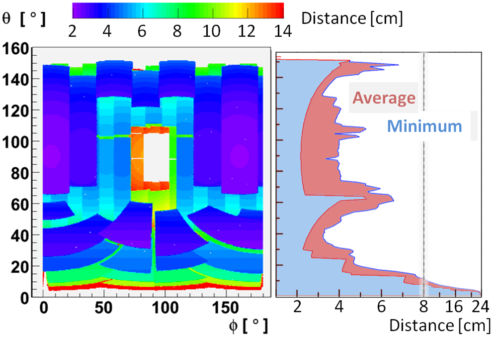
Besides a sufficient number of MVD hits for each particle track, a minimum distance of the first hit point with respect to the nominal IP is crucial for the physics performance of the detector. A 2D illustration of the absolute distance of the first hit point to the origin is given in figure 6.21, on the left. Next to it, on the right, corresponding 1D profiles along the the polar angle are added. They show the minimum and the averaged value obtained within the full azimuthal angle. Results indicate that a distance of less than 4 cm can be reached within a wide range of the covered solid angle. Minimum distances to the nominal interaction point are obtained in the barrel part and at polar angles around 30∘ are in the order of 2 cm.
6.6.3 Material Budget
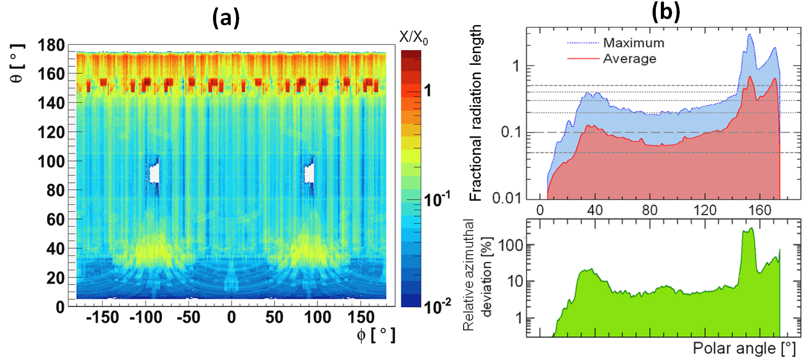
The introduction of the MVD is inevitably connected to some detrimental effects given by scattering and energy straggling of charged particles as well as the conversion and attenuation of photons inside the detector material. The impact of the introduced material can be quantitatively described by a resulting fractional radiation length, , which is accumulated in all traversed volumes :
| (6.14) |
where and are the specific radiation length and the density of the material defined for the volume , respectively, and corresponds to the traversed path length therein. In the further discussion the corresponding value of the material budget will be given in a percentage of one full radiation length, %, if or in multiples of if .
The following studies about the material budget are based on the comprehensive MVD model, which has been introduced in chapter 6.2. For the extraction of a material map, virtual particles (“geantinos”) were propagated through the detector. The fictitious “geantino”particle undergoes no physical interactions but flags boundary crossings along its straight trajectory. Two million events were simulated starting from the origin (;;) = ](0;0;0) with an isotropic emission over the polar angle, , and the azimuthal angle . Further on, the effective path lengths in all traversed volumes () were identified for each propagated geantino. The fractional radiation length () was then calculated based on the given material definition of the volumes according to equation \eqrefeq-FractRadLength.
In figure 6.22 (a) the obtained material map of the MVD is given in the representation of the fractional radiation length, which is plotted colour-coded against both initial emission angles. Corresponding profiles along the polar angle are shown in figure 6.22 (b). They are obtained for a bin size of = 1∘. Resulting numbers for the average and the maximum fractional radiation length within each interval are shown at the top. The standard deviation of all values normalised to the corresponding mean value is plotted below. This ratio is a measure of the isotropy in the material distribution along the integrated azimuthal angle. The obtained material distribution indicates a very low material budget of the MVD in the physically most important region at polar angles smaller than 140∘. Corresponding values stay mainly well below 10% and the overall material map shows a rather isotropic occupancy with relative fluctuations of not more than 10%. Larger deviations are located between and as well as in the very backward region (), which generally exhibits an increased material budget with peak values of several radiation lengths. Further details of the material map will be discussed in the following paragraphs.
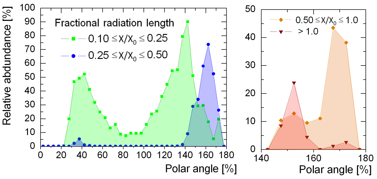
First of all, the focus is given to local hot spots, i.e. regions with an enhanced fractional radiation length. Figure 6.23 illustrates the azimuthally integrated distribution of such hot spots along the polar angle. The given relative abundance is defined as the fraction of counted tracks, , for which the obtained value of stays in the specified range, divided by the overall number of tracks, , to be expected within an interval of . The latter, , is given by the percentage of the covered area in the diagram multiplied with the total number of simulated events.
Different intervals for the fractional radiation length were chosen to classify hot spots with respect to the average value obtained in the sensitive detector region (). A lower limit for the definition of a hot spot is given by
| (6.15) |
where and represent the mean values of the fractional radiation length and the standard deviation within the intervals, respectively. Both of them are extracted from the 1D profiles shown figure 6.22. Finally, four different categories have been specified. The first category (I) defined in an interval of rather describes larger fluctuations to the averaged value. Moderate hot spots of category II are in the order of and . The last two categories III and IV account for hot spots with a very large value below and above one full radiation length , respectively.
Compiled results in figure 6.23 indicate that hot spots of category II to IV are basically outside the sensitive detector region of the MVD. An exceptional contribution of moderate hot spots (category II) in the order of 5% can be located between and . All other hot spots of the second, third and fourth category are located in the upstream region between and . Fluctuations of the material map included in category I are mainly spread over the sensitive detector region. The maximum of this distribution shows up at .
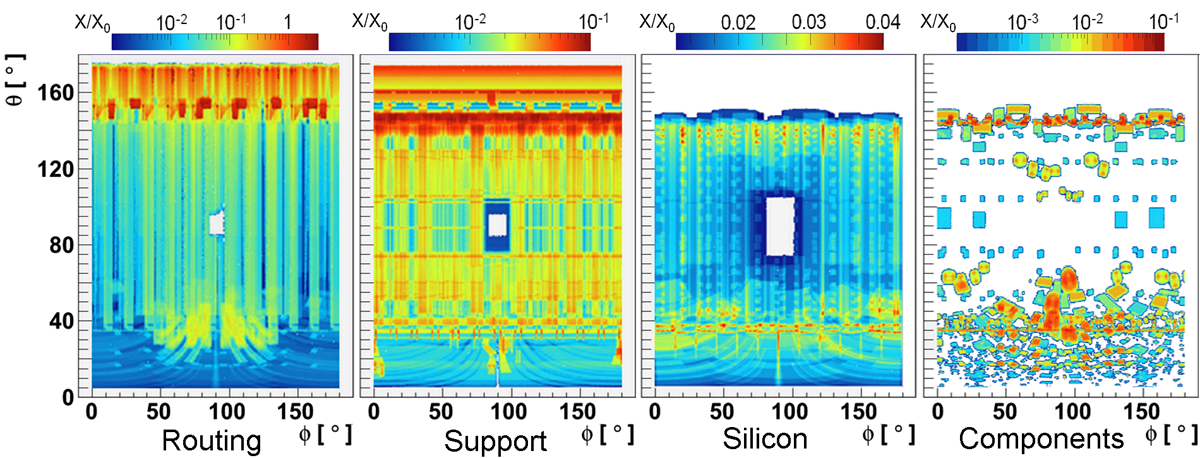
In order to obtain a better understanding of the resulting pattern in the material map it is useful to perform a separate analysis of different detector parts. Therefore, only the individual components of interest were switched on during the simulation. In a first step, the four main substructures of the MVD model have been chosen. These main parts are (cf. figure 6.3):
- Silicon:
-
Sensor elements and associated readout chips
- Support:
-
Global and local support structures
- Routing:
-
Service structures for sensors and \frontendchips including supply and data cables as well as cooling pipes
- Components:
-
Electronic and cooling connectors as well as additional SMD components
The individual contributions of these substructures are disentangled in figure 6.24. In comparison with figure 6.22 it is evident that the most significant impact on the material map originates from the routing part. It delivers the obvious jump to a larger fractional radiation length at polar angles above 140∘ and also includes hot spots with maximum values of several . These enhancements are related to the fixed routing scheme of the inner barrel layers along the opening beam pipe in upstream direction in combination with the generally increased incident angle of tracks traversing the circularly arranged service structures. In the forward region (2550∘), the routing of the pixel disk services at the top and bottom is clearly visible. It results in a partial increase above (cf. figure 6.23) thus defining the maximum material budget in the sensitive detector region. Besides, average values therein level around 5%.
Compared to the routing part, maximum values of all other sub-structures in the 2D distribution fall short by more than one order of magnitude. Support structures contribute with 1% to 3% in the active detector region. Moreover, higher values reflect the load pick-up of the main building blocks, which is concentrated in upstream direction at polar angles above 140∘. A maximum of approximately 5% and 10% is given below (forward part) and above (barrel part), respectively. The most homogeneous material occupancy around 2% is given by the silicon part. It shows a typical -modulation reflecting the incident angle of straight lines originating from the nominal interaction point. A further increase at smaller polar angles is related to the enlarged number of individual detector layers in forward direction. Finally, the resulting pattern of the introduced components defines a very anisotropic distribution. While the averaged number remains relatively small, maximum values of around 5% are reached at singular points. Most of them are related to cooling connectors needed to change from steel pipes to flexible tubes.
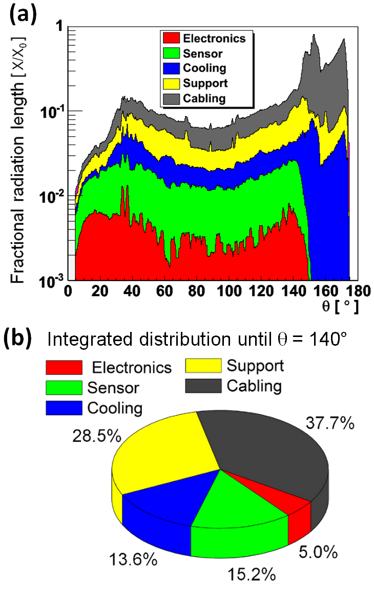
For the evaluation of different hardware developments in terms of their impact on the overall material budget a slightly modified representation is used, which re-orders the different volumes of the MVD model to functional groups:
- Sensors:
-
Silicon pixel and strip detectors
- Electronics:
-
Readout chips, SMD components and electronic connectors
- Cabling:
-
Routed supply and data cables (core and insulation)
- Cooling:
-
Coolant, pipes and tubes as well as cooling connectors
- Support:
-
All support structures (as defined before)
The stacked diagram in figure 6.25 (a) illustrates the individual contributions for each of these functional detector parts along the polar angle. Plotted values represent the azimuthally averaged fractional radiation lengths within an interval of . Besides some accumulation effects in the very forward region, the proportions between all parts remain relatively constant within the sensitive detector region (140∘). In figure 6.25 (b) their percentage on the overall budget is presented in a pie chart. The biggest amount of material is delivered by the cables (38%) and the support structures (29%). The dominating part (70%) of the material budget of the cabling part splits into 78% and 22% for the supply and the data cables, respectively. The introduced silicon sensors assuming standard total thicknesses of 200 m and 300 m for the pixel and the strip detectors, respectively, account for only 15%. The cooling system adds another 14% to the material map and the impact of the electronics stays in total rather small (5%). However, it should be recalled that the discussion on integrated distributions does not supersede a careful evaluation of the 2D map as done before.
In summary, the obtained composition of the material budget is typical for inner silicon tracking systems of hadron physics or high-energy physics experiments. In case of \Panda, complications for a minimised material budget are given by the overall routing scheme, which requires the upstream routing of all services thus implying e.g. folded service lines for the pixel disks, and the DAQ concept, which is based on a triggerless readout thus increasing the material due to the higher functionality of the readout chip and the larger amount of data to be handled. Even though the total amount of material for all service structures can be kept in an acceptable range. This fact results from an optimised powering scheme for the readout electronics, which decreases the required core cross section of the supply cables, and the use of ultra-thin cables based on an Aluminum core. Both reduce the overall material budget by roughly 45%. Moreover, a significant minimisation is given by the use of lightweight carbon support structures with a tailored design, i.e. larger cut-outs and sandwiched structures with Rohacell. Further improvements, which are not included in the presented studies, are related to thinned silicon detectors, the use of aluminum supply cables surrounded by just a thin copper layer and the implementation of a higher data concentration. The maximum achievable reduction in best case is expected to be in the order of 25%. A detailed discussion of these point can be found in [PhD-Tesis_Wuerschig].
6.6.4 Rate Estimation
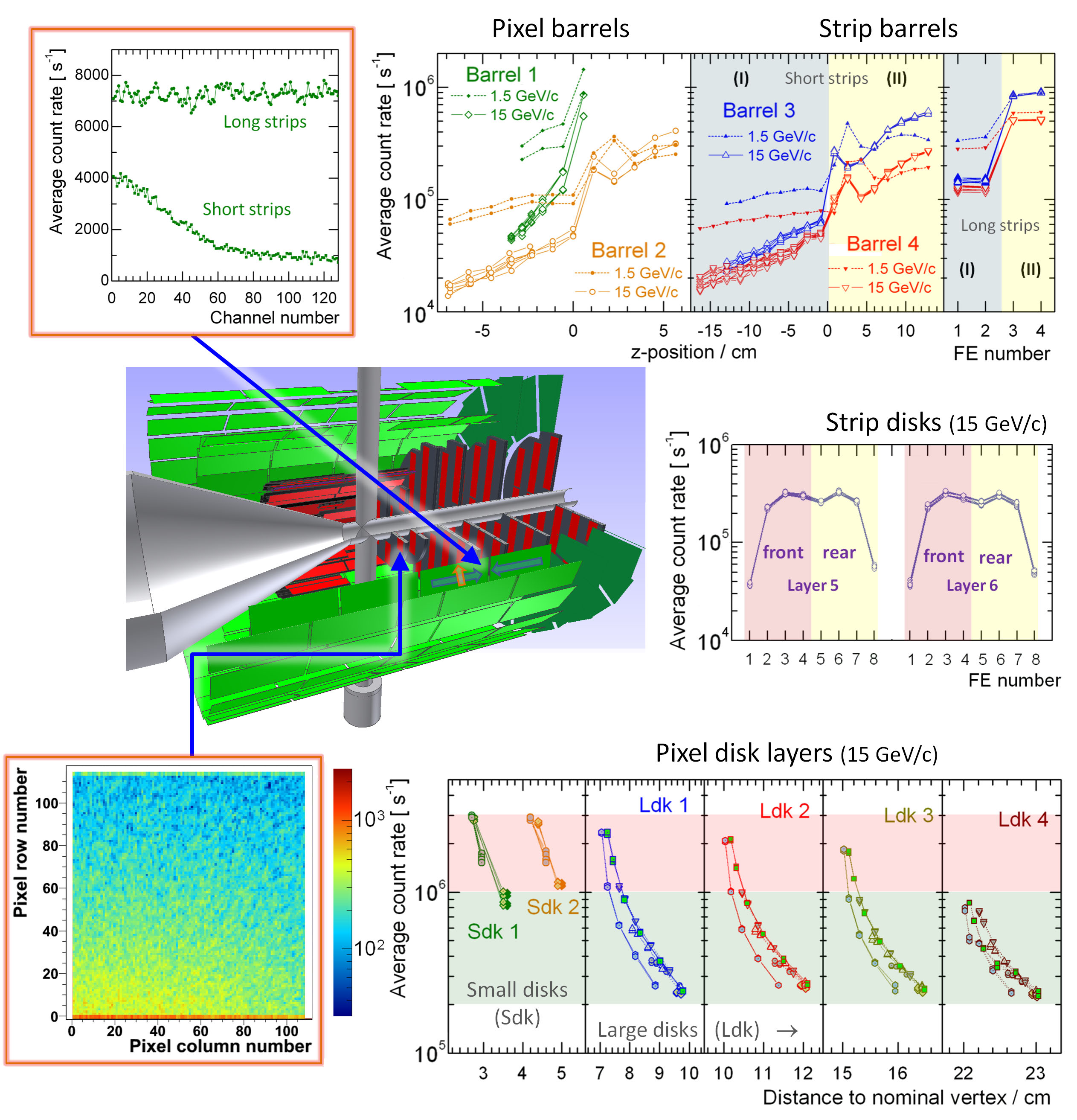
For the MVD as innermost subdetector of \PANDA,
an evaluation of the expected count rates in different detector regions
is from utter importance for the development of all readout electronics.
Extracted numbers result from the initial conditions of the experiment,
i.e. the particle distribution in the reaction channel
(cf. figure 2.2, chapter 2.3)
and the beam-target interaction rate taken as basis for the calculations.
In a first approximation, the latter can be correlated with
the nominal \PANDAinteraction rate, which is given by 2 s-1.
With the time-averaged information it is possible to extract
the hit occupancy in different detector regions
and the overall data load expected to be handled by the MVD.
For a reasonable estimate on peak rates occurring on single readout channels and on
frontend level,
variations of the beam-target interaction on a shorter time scale must be considered.
A detailed count rate study for reactions has been performed at minimum (1.5 \gevc), maximum (15 \gevc) and an intermediate beam momentum of 5 \gevc [PhD-Tesis_Wuerschig]. A large statistical sample of two million DPM events were simulated for each of the three setups. Generated particles were propagated through the detector within the PandaRoot framework. Moreover, the created hit points in the detector were digitised as described in chapter 6.3.2. In the further analysis only binary hit information, i.e. the IDs of sensor and \frontendas well as the number of the readout channel, was stored thus allowing an unambiguous allocation of each hit point in the detector. The summed hit counts were then multiplied with the nominal \PANDAinteraction rate in order to obtain the time-averaged count rate. The given number for an individual readout chip results from an integration of all associated readout channels. In the same way, average count rates for individual sensors are defined by the contribution of all connected readout chips. The hit occupancy for different detector parts is then given by the accumulated count rates of all sensor elements therein.
Obtained results for the count rate distribution on \frontendlevel and the individual contributions of single readout channels are summarised in figure 6.26. Due to the distinct emission of particles in forward direction with increasing beam momentum, the highest count rates inside the MVD occur at maximum beam momentum in the inner pixel disk layers. Upper limits of three million counts per second (Mcps) are obtained for individual pixel readout chips located at the inner sectors of the small pixel disks. Also at the inner rims of the subsequent pixel disks, average count rates stay at a high level between 1.9 Mcps and 2.5 Mcps. At outer radii values drop quickly by one order of magnitude. For the two innermost pixel disks the situation is more challenging because all the \frontendshave to cope with a high count rate of more than 1 Mcps. These special conditions require a sophisticated cooling concept for the readout electronics (cf. chapter 5.6.1), which is crucial for a stable operation. The highest count rates for readout chips in the strip disks are in the order of 0.3 Mcps. The shorter strips at one sensor edge of the trapezoidal sensors lead to a lower count rate for the \frontendat the outermost position. This effect is mirrored at the opposite sensor side.
In contrast to the forward part, the occupancy in the barrel part increases with lower beam momentum due to the increased number of particles emitted at larger polar angles. The distributions at highest and lowest beam momentum are plotted in figure 6.26. The impact of the slow elastic recoil protons results in a local maximum for \frontendslocated just behind , which corresponds to the observed peak in the overall particle distribution shown in 2.2. Due to the orientation along the beam axis, the average count rates of long strips stay for one sensor always above the ones of short strips. Upper limits for the strip part are obtained in the third barrel layer at minimum beam momentum. Assuming an interconnection of the two foremost sensors, which is one of the possible solutions envisaged to reduce the total number of readout channels, maximum values for the strip \frontendsstay slightly below 1 Mcps. This value is slightly exceeded for the foremost readout chips of the first pixel layer, thus defining the maximum average count rates occurring in the overall barrel part. In the upstream part () obtained values do not exceed a level of 0.1 Mcps.
Pixel and strip readout chips with the maximum occupancy also contain readout channels with the highest individual count rates. In case of the strip part, the distribution over all connected readout channels ranges between 7000 counts per second (cps) and 8000 cps. For the pixel part a more anisotropic occupation on the pixel readout chip is obtained. Values for single pixel cells differ by roughly one order of magnitude with an upper limit of roughly 1200 cps. The increased count rate at the top and the bottom of the pixel matrix stems from an enlarged pixel size, which is implemented to counter-balance the passive edge of the readout chip.
| Barrel | Forward | Sensor | \Frontend | Readout | |
| part | part | level | level | channel | |
| Pixel part | |||||
| Digitised hits | 6.7 4.2 | 16.6 32.2 | 0.89 | 0.29 | |
| / [106] | (1.5 15) \gevc | (1.5 15) \gevc | 0.04 | ||
| Average count rate | 233 364 | 8.9 | 2.9 | 0.002 | |
| / [Mcps] | (1.5 15) \gevc | 2.1 | |||
| Expected data rate | 45 | 17 | |||
| / [MB/s] | |||||
| Estimated peak rate | 4.0 | 0.01 | |||
| / [Mcps] | 14.5 | ||||
| Strip part | |||||
| Digitised hits | 21.1 17.6 | 5.0 8.4 | 0.30 | 0.09 | |
| / [106] | (1.5 15) \gevc | (1.5 15) \gevc | |||
| Average count rate | 418 416 | 4.8 | 1.5 | 0.013 | |
| / [Mcps] | (1.5 15) \gevc | ||||
| Expected data rate | 29 | 9 | |||
| / [MB/s] | |||||
| Estimated peak rate | 2.0 | 0.02 | |||
| / [Mcps] | 5.5 | 0.07 | |||
frontend and channel level represent the maximum values obtained for a single element. Mean values of all elements in the corresponding setup are indicated with .
The most important results of the presented count rate study are compiled in table 6.3. For the integrated pixel and strip part an upper limit on the average count rate is given by 360 Mcps and 420 Mcps, respectively. In case of the strip part final numbers contain a factor of [PhD-Tesis_Wuerschig], which considers an induced charge sharing between neighboring channels, i.e. a minimum number of two activated strips per hit. Such technique based on a smaller substructure with interstitial floating strips is envisaged for the silicon strip detectors in order to improve the spatial resolution. Taking into account a size of 40 bit for the output format of the hit data (cf. chapter 5.4.1) it is possible to estimate the corresponding data load. By introducing a scaling factor, byte 555Compared to the 5 bit format defined in chapter 5.4.1 an additional safety bit was added to estimate an upper limit, obtained numbers for the average count rate can be translated into a data rate given in megabytes per second (MB/s). The maximum data load of roughly 4.7 GB/s is expected at highest beam momentum, at which the contribution of the pixel and the strip part are in the same order of of magnitude.
Fluctuations of the total number of registered hits on a short timescale deliver increased peak rates, which have to be buffered by the readout electronics. As a first approach, the intrinsic change of the instantaneous luminosity profile during the operation cycle can be taken to deduce a lower limit on the occurring peak rates. According to model calculations for the \HESR [HESR-BeamDynHinterberger] it is given by an increase of , which results from the ratio of the luminosity at the start of the data taking period to the cycle-averaged value. Additional fluctuations may be introduced by variations of the effective target thickness and the microscopic structure of the beam. An initial rudimentary study for the use of a pellet target at \PANDA [HESR-PelletPeakLumi] allows for a very rough estimate of an upper limit, which results in a scaling factor of .
| Pixel | Strip Barrel | Strip Disks | |
|---|---|---|---|
| Readout size | 100100 m2 | 130 m | 65 m |
| Stereo Angle | – | ||
| Noise | 200 | 1000 | 1000 |
| Threshold | 1000 | 5000 | 5000 |
| Charge Cloud | 8m | 8 m | 8 m |
Further simulations included in [PandaNote7-Rate], [PandaNote4-Rate] have been performed to study the possible effects of antiproton-nucleon reactions on the expected count rates inside the MVD. Results indicate that the extracted hardware specifications based on the numbers as given in table 6.3 suffice for a compliance of the required detector performance under these conditions.
6.7 Resolution and Performance Studies
This section contains studies dealing with the performance of the MVD as standalone detector and in the whole \Pandasetup. For comparable results, a set of default parameters, see table 6.4, has been used.
6.7.1 Hit Resolution
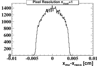
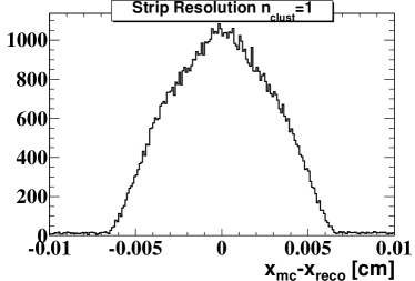
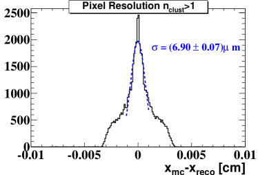
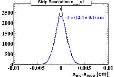
A good position resolution of each hit on a sensor is mandatory for a good momentum and vertex reconstruction. To have a clean sample, only charged pions with a momentum of 1 \gevchave been used, covering the whole azimutal angle range while the polar angle covers 7∘ to 140∘. The figure 6.27 shows the resolutions per sensor type and by cluster multiplicity. For the case of one digi per cluster, the resolution is limited by the readout structure size (100 m for the pixels, 130 m and 65 m for the strips). When the charge weighted mean is used, the achieved single hit resolution largely improves ( m for the pixels and m for the strips).
6.7.2 Vertexing Performance on Pions
Several scans were performed to characterize the vertexing performance of the MVD. Four pions (two and two ) of 1 \gevcwere propagated through the detector from a common vertex distributing homogeneously the four particles along the and ranges (, ). The vertices were set in different regions to map the resolution and to perform systematic studies (10.000 simulated events per point):
-
•
longitudinal scan: moving the vertex along the longitudinal (z) axis in the range [-1,+1] cm;
-
•
circular scan: positioning vertices along a circle with a radius 0.1 cm in the transverse (x-y) plane
-
•
radial scan: changing the distance between (0,0,0) and the vertex moving along a radius in the transverse plane.
These studies were realized using the MVD, the STT, the GEMs and the forward tracker. The tracking was performed merging the information provided by the barrel and the forward spectrometers. A Kalman filter was applied to tracks measured in the barrel spectrometer, correcting for energy loss and scattering occurring in the detectors (see section 6.4). Forward tracks were reconstructed using the ideal pattern recognition and smearing the track parameters according to resolution and efficiency foreseen for the forward tracker. Finally the POCA vertex finder (see section 6.4.4) was applied to track candidates, obtaining the reconstructed position of the vertices.
All the scans showed a similar behavior: the vertex resolution achieved for the x coordinate is worse than y. This is not expected due to the symmetry of the MVD geometry. The reason of this discrepancy is the design of the inner barrel layers of the MVD, which is limited by mechanical constraints. The top and bottom regions close to the nominal interaction point cannot be covered with pixel modules in the range .
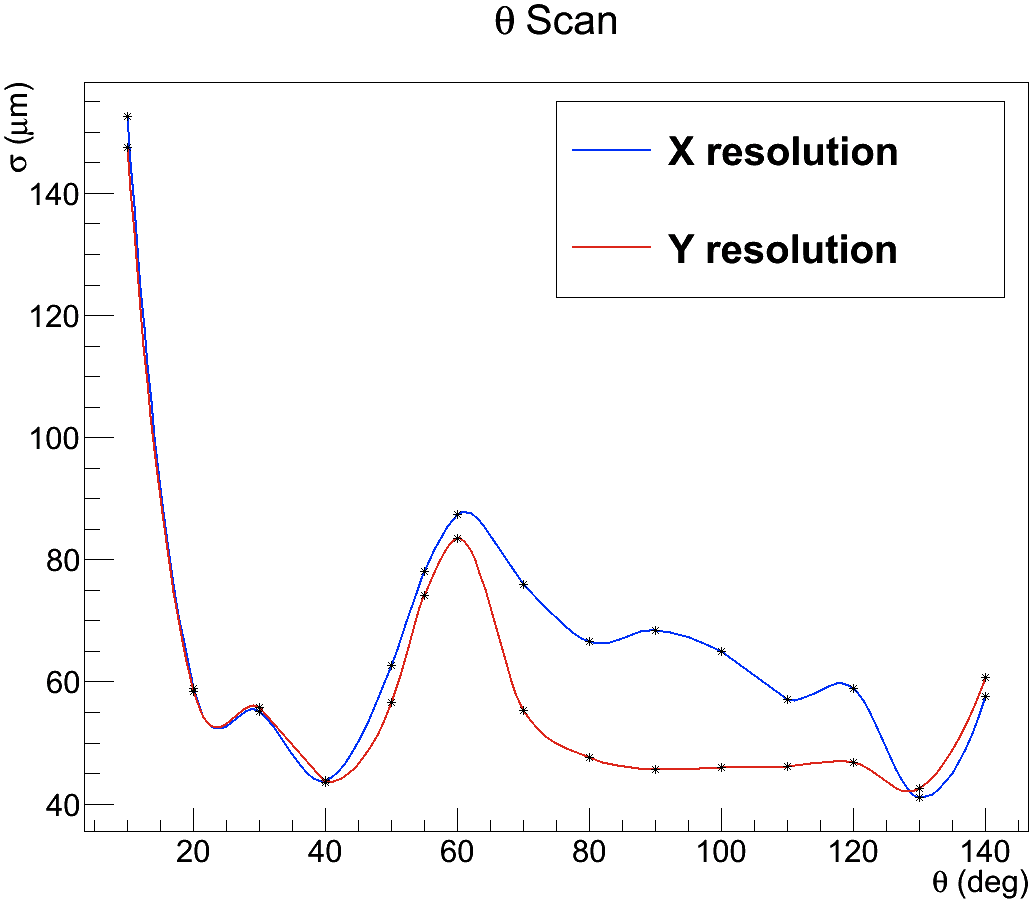
This results in a different precision in the determination of the coordinates of the reconstructed vertices, which is significant in this portion of solid angle. Figure 6.28 shows the x and y resolutions obtained with selected values for the four pions. A detailed analysis of the origin of this different behavior can be found in the appendix C. The studies presented this section were performed covering homogeneously a wide range. This is the reason why in the results a significant difference appears between the x and the y vertexing performances. Most of the physics channels of interest for the experiment foresee mainly decays in the forward region of the detector, therefore the x-y different performance at big angles will not influence most of the physics studies. For example all the results of the next section (6.8) show the same resolution for the x and y vertex reconstruction.
Results of the Scans
The longitudinal scan (figure 6.29) shows that vertex resolution values are quite stable in the range [-5,+5] mm, where the pattern recognition for primary particles is foreseen to work efficiently. The circular scan (see figure 6.30) confirms a good -uniformity of the performance expected on the basis of the detector geometry. In figure 6.31 the effects of a movement along a radius with and cm are shown. The resolutions are not severely influenced by this kind of shift as long as one stays at distances below 1 cm from the nominal interaction point. There the vertexing starts to show worse performances.
The momentum resolution is much less effected by changes in the position of the vertex and it stays constant within a few per mill in all the performed scans (see figure 6.32).
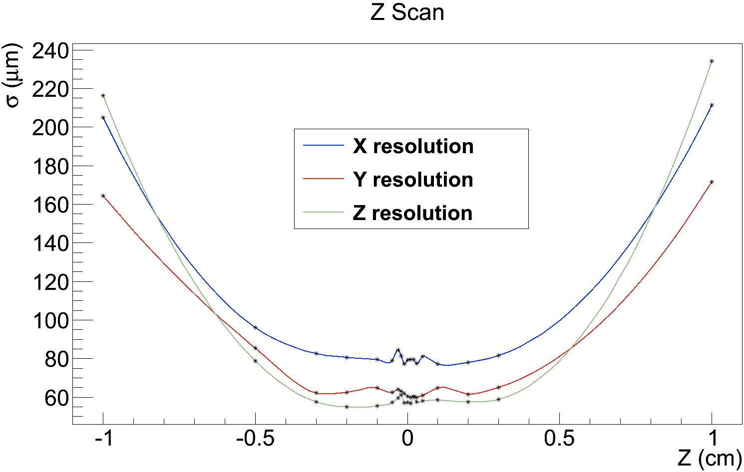
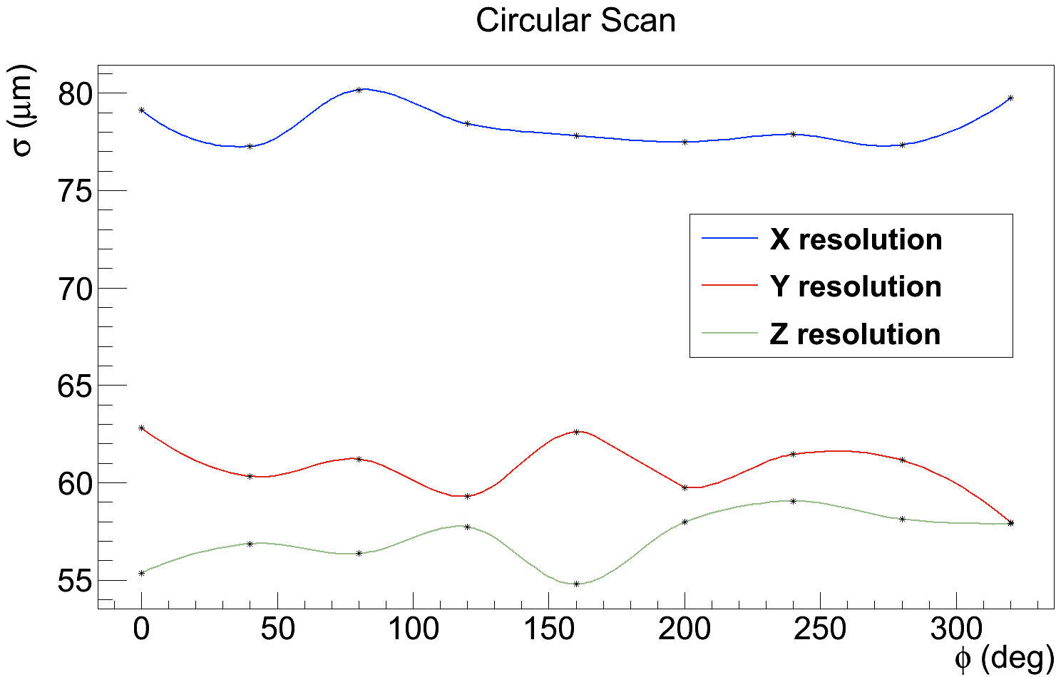
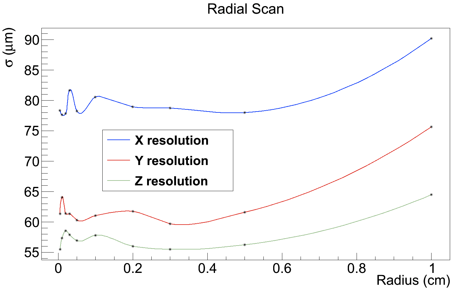
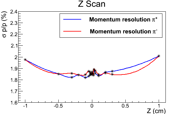
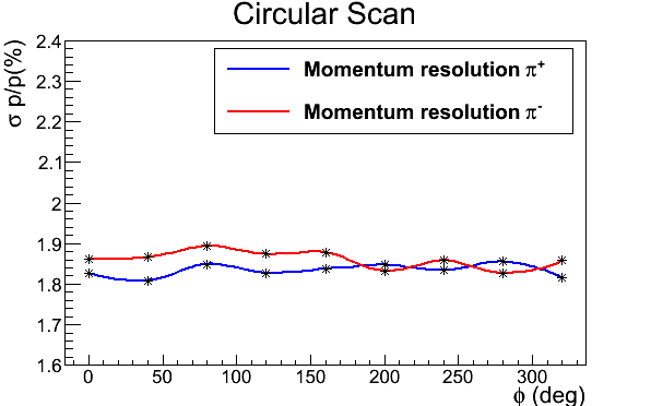
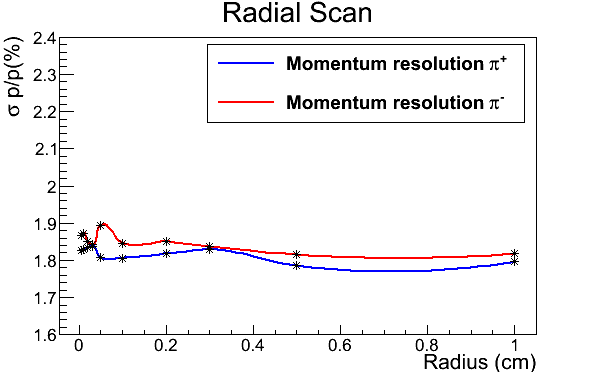
6.8 Physics Channels Analysis
The tasks of the \Mvdare mainly to provide high tracking performance close to the interaction zone. We report three physics benchmark cases where the performance of the \Mvdis monitored. First we have particles decaying directly in the interaction point (), and in the second case particles which decay further away from the interaction point (\Dmesons).
6.8.1 Detector Setup
In the physics channels we chose the following geometric setup. Active components:
-
•
\Mvd
: 4 barrel layers and 6 disks
-
•
STT: 1.5 m long, with skewed layers
-
•
GEM: 3 stations
-
•
FTS: 6 forward tracking straw stations
For these elements hit digitization and reconstruction is performed. In the barrel spectrometer part the combined STT+\Mvd+GEM pattern recognition with a Kalman Filter track fitting is used, with the default particle hypothesis being muons. In the forward spectrometer a Monte-Carlo truth based tracking is applied with a 95% efficiency and gaussian smearing of in momentum as well as m in position. Realistic particle identification algorithms are not used, in order to have results independent from them. To identify particles the Monte-Carlo information is used.
The following components were present as passive material, thus contributing to the material being present, excluding the time consuming digitization processes of these components not being relevant in these studies.
-
•
Pipe Beam-Target cross (passive)
-
•
Disc DIRC
-
•
Barrel DIRC
-
•
EMC crystals
-
•
Solenoid and forward dipole magnet, including flux return yokes and muon chambers
The simulations of physics channels were done with the PandaRoot “trunk” revision number 12727 from July, 18 2011, using the “may11” release of the external packages.
6.8.2 Benchmark Channel:
The first test has been performed reconstructing the following reaction:
Running a full analysis and performing a vertex fit on the candidates it was possible to determine the vertex resolution. Figure 6.33 shows the distributions of the x and y coordinates of the reconstructed vertices. The resolution in z is slightly worse ( m, while m and m) due to the forward boost of the decay.
The overall vertex reconstruction is excellent.
Figure 6.34 shows the mass distribution obtained for the and the candidates, respectively. The masses obtained fitting these distributions are in full agreement with the expected values.
Figure 6.35 shows the missing mass of the reaction at the peak, from which the signal emerges. The signal obtained in this way is much narrower than that obtained by the invariant mass of the lepton pairs (figure 6.34).
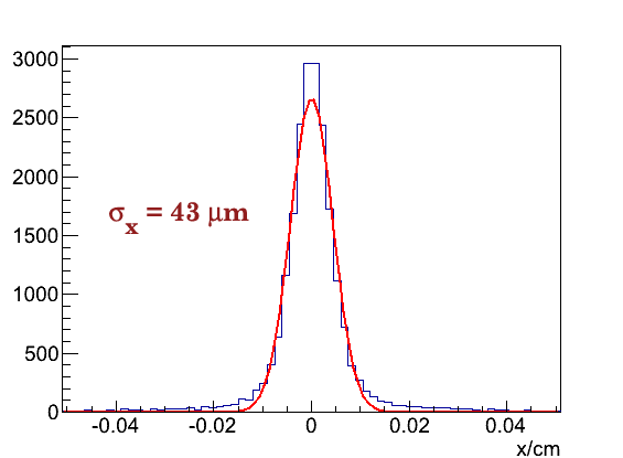
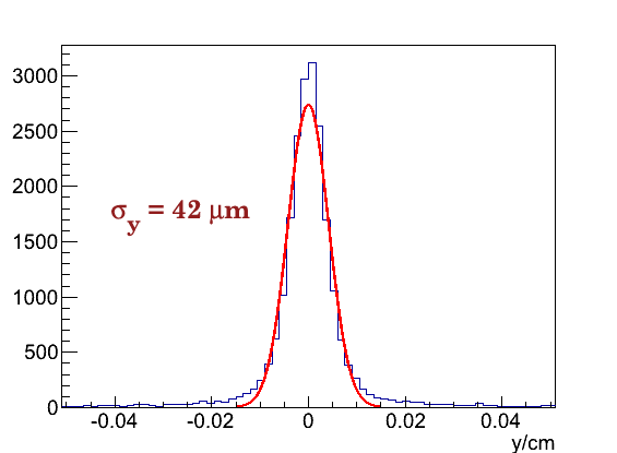
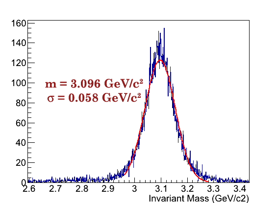
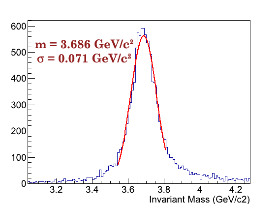
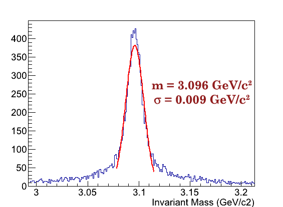
The decay of the into has been studied in the same situation. This decay is more effected by multiple scattering than the muonic one. Therefore some selections on the reconstructed candidates can improve the final results. Only and candidates matching the allowed phase space regions666This cut was based on the MC-true phase space distributions for this decay were taken into account for the rest of the analysis.
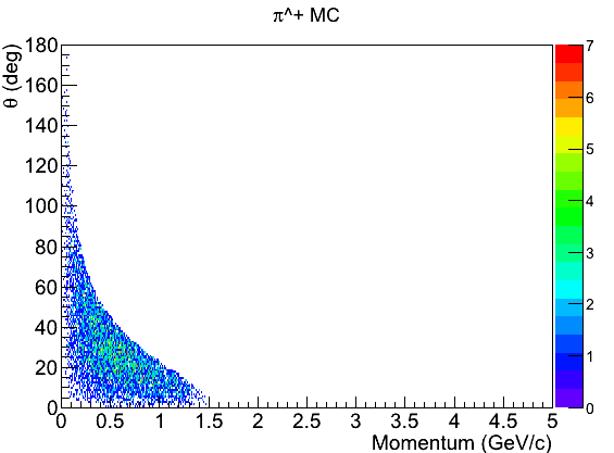
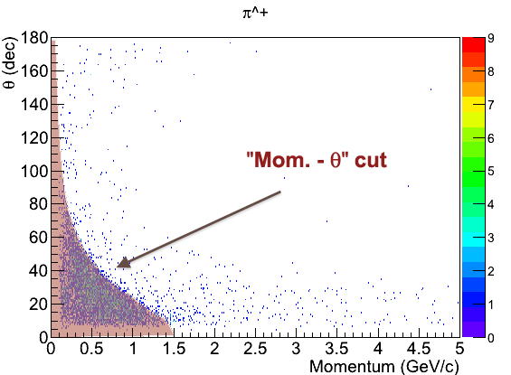
Figure 6.36 and figure 6.37 show the MC prediction for the polar angle and momentum distributions compared with what is obtained from the reconstruction. Two colored bands highlight the specific cuts applied on the kinematics of the track candidates.
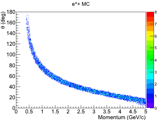
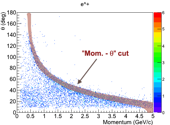
Applying these selections, candidates have been reconstructed. The distributions of the reconstructed vertex positions are shown in figure 6.38.
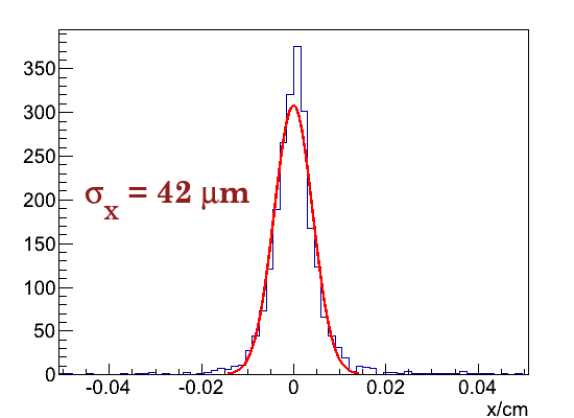
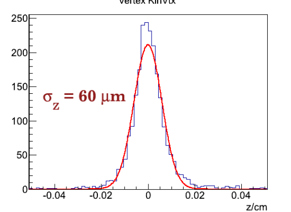
Figure 6.39 shows the invariant mass of possible candidates and the missing mass built by the measured pions (which obviously does not depend on the the decay mode).
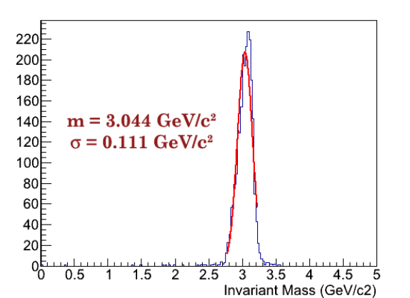
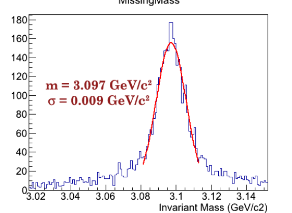
Figure 6.40 shows the distribution of the reconstructed vertex positions. These vertices are calculated combining four particles. Therefore more constraints are applied than in the case of the vertex. This results in a better z resolution due to the forward boost of the system. These considerations are based on the fact that both the and the decay immediately in the interaction vertex.
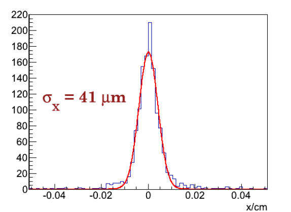
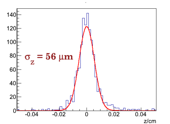
The invariant mass of the candidates are shown in figure 6.41 where the results of a Gaussian fit on the peak are reported.
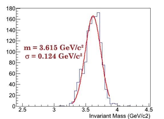
Since candidates are obtained combining ones with a and a , which both have to satisfy track quality requirements, the final total number of reconstructed is smaller than the available statistics.
6.8.3 Benchmark Channel: \Dmesons
In order to explore charm physics in \Pandathe reconstruction of \Dmesons is a crucial point. The biggest challenge is to reduce the background from the signal channels, which have typically a low cross section. Because the decay lengths are m for the charged and m for the neutral ground state \Dmesons, a selection by the decay vertex is envisaged.
The charged ground state mesons decay by 9.4% branching fraction into a final state with three charged particles (, see [PDG:2010]). It is convenient to have only charged particles in the final state to be less dependent on other detector components in this study. In the exit channel six charged tracks then have to be reconstructed:
For this study 99200 signal events have been simulated at 9 \gevcincident antiproton momentum, enabling a large maximal opening angle between the two mesons (see figure 6.42).
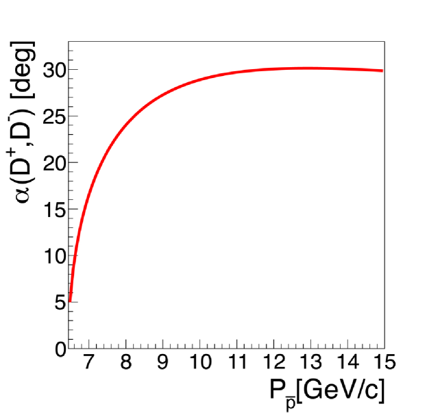
Furthermore a set of 344525 non-resonant background events was simulated featuring the same final state: .
| \Dp/\Dm | comb. | nonres. | \Dz/\Dzbar | comb. | nonres. | |
| Simulated events | 99200 | – | 344525 | 98800 | – | 198125 |
| Simulated \D’s | 198400 | – | (689050) | 197600 | – | (396250) |
| \D’s After reconstruction | 120835 | 67039 | 688188 | 135024 | 27161 | 322771 |
| \mevccMass window | 61579 | 21963 | 67645 | 102763 | 2232 | 23301 |
| Vertex r and z cut | 15004 | 689 | 1060 | 17255 | 194 | 543 |
| 4C kinematic fit | 1058 | 25 | 0 | 1592 | 18 | 2 |
| Suppression factor (fits & cuts) | 8.810-3 | 3.710-4 | 1.510-6 | 1.210-2 | 6.610-4 | 6.210-6 |
| Suppression factor (total) | 5.310-3 | 1.310-4 | 1.510-6 | 8.610-3 | 9.110-5 | 5.110-6 |
After the reconstruction 60.9% of the original \Dmesons survived with 33.8% of additional combinatorial background. The exact numbers are compiled in table 6.5. A rather wide mass window cut of 150 \mevccaround the nominal charged \Dmass (taken from [PDG:2010]) was applied to reduce the non-resonant background by a large factor. Cutting on the vertex z coordinate (POCA) of the \Dcandidates (478 m ) and on the “distance” (see section 6.4.4) calculated by the POCA finder ( m), much of the combinatorics as well as the non-resonant background is removed. The vertex resolution values are given as the gaussian fit’s width in table 6.6. The three available vertex finder/fitter algorithms have been used. With a precise vertex position it is possible to measure the decay length of the \D’s. We found () m which is in agreement with the PDG value of m ([PDG:2010], see figure 6.43). This includes also a correction for the tracking acceptance. The POCA finder gives a good resolution, hence it was used to finally determine the mass resolution (shown in figure 6.44), which is 20.4 \mevccby reconstruction only, and 8.7 \mevccafter the fits. The combinations of both \Dmesons in each event are fitted with a four constraint kinematic fit. Here the knowledge of the initial states four-momentum, i.e. the ideal beam, is introduced. After a cut on the fit’s probability () most of the background sources are suppressed and the \Dmass resolution is improved significantly (see figure 6.44).
| \Dp | Poca | PRG | KinVtx |
| m | 56.9 | 86.1 | 46.9 |
| m | 56.3 | 84.8 | 46.1 |
| m | 113 | 125 | 93.2 |
| \Dm | Poca | PRG | KinVtx |
| m | 57.4 | 85.3 | 46.3 |
| m | 56.0 | 84.4 | 45.7 |
| m | 110 | 123 | 94.1 |
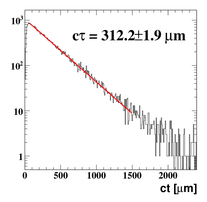
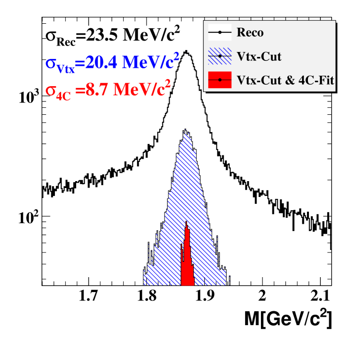
An important number is the signal-to-background ratio. The number of simulated events has to be scaled by the channel cross section accordingly. The non-resonant background production cross section can be estimated to 23.4 (value at 8.8 \gevcin [Hill:1983se]) and for the signal to 0.04 [Kaidalov:1994mda]. Using the suppression factors from table 6.5 and the final states branching fraction, one can estimate:
| (6.16) |
Neutral ground state \Dmesons decay by 3.89% into a two charged particle state (see [PDG:2010]):
Having only two particles to form the \Da higher reconstruction efficiency is expected, due to the smaller number of particles which have to be inside the detectors acceptance. Out of the 98900 simulated signal events, 68.3% where reconstructed while additional 13.7% of combinatoric background is found. The numbers of surviving events after the cuts are compiled in table 6.5, while the vertex resolutions with the three fitters/finders are presented in table 6.7. Similar to the charged \Dmesons one, the mass resolution achieved is 24.5 \mevccbefore and 5.8 \mevccafter the fits (see figure 6.46).
| \Dz | Poca | PRG | KinVtx |
|---|---|---|---|
| m | 47.3 | 57.9 | 44.3 |
| m | 45.6 | 51.6 | 42.9 |
| m | 88.4 | 94.9 | 90.2 |
| \Dzbar | Poca | PRG | KinVtx |
|---|---|---|---|
| m | 47.5 | 58.3 | 44.6 |
| m | 46.3 | 51.9 | 43.5 |
| m | 88.4 | 94.1 | 89.3 |
Extracting the decay length of the neutral \D’s we find () m which agrees with the PDG’s input value m [PDG:2010].
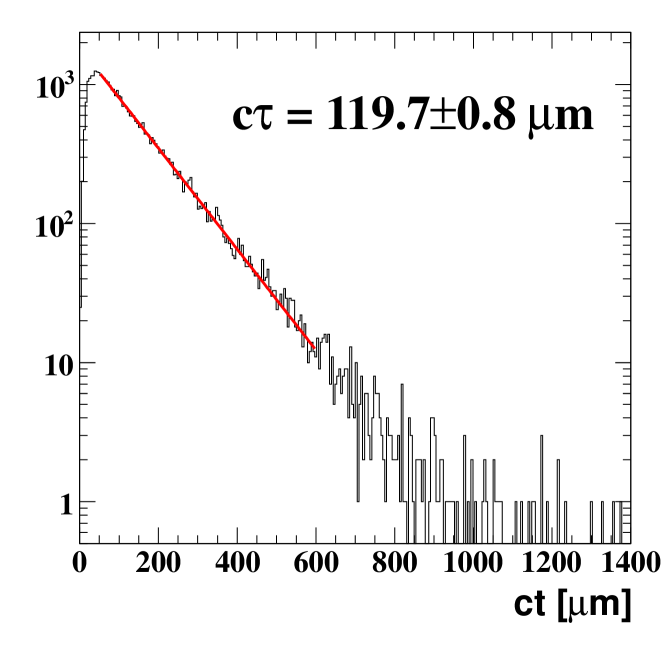
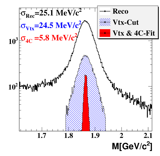
Calculating the signal-to-background ratio we approximate the cross section for the signals by using the charged \Dmesons case, 0.004 and 8.5 (value at 8.8 \gevcin [Hill:1983se], see also figure 6.47) for the non-resonant background. The resulting signal-to-background ratio, using the numbers from table 6.5, is:
| (6.17) |
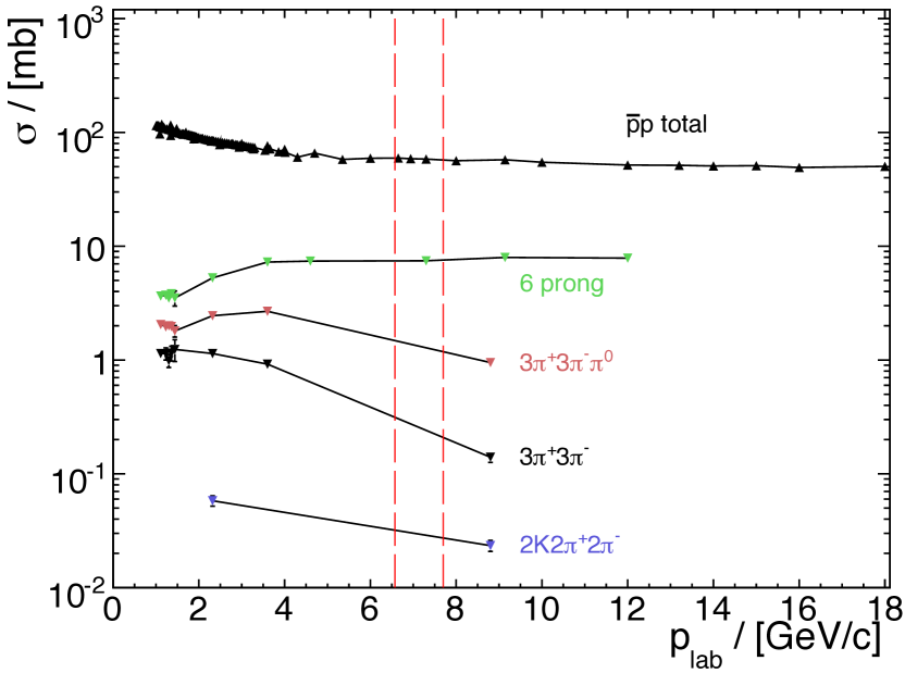
6.8.4 Considerations About the Vertexing
The physics channels studied in the previous sections proof the \Mvdvertexing capabilities. These results are not affected by the different x-y resolutions mentioned in section 6.7.2, since all the decays are boosted forward, where the vertexing performance of the \Mvdis homogeneous (see figure figure 6.28). The reconstruction of candidates showed the vertex resolutions achievable with two-body leptonic decays ( 43 m, 60 m). The study of the full reaction demonstrates the improvement of the z vertex reconstruction with a bigger number of constraint (more tracks taken into account for the vertex determination). This effect is more evident in z the in the other coordinates due to the forward boost of the system. The detailed study of the effect of several analysis techniques on the analysis of charged and neutral \Dmesons highlights how crucial the \Mvdis when dealing with small cross sections and in the cases where the topology of the background are quite similar to the one of the signal under study. Vertex cuts result in being crucial for the background suppression (for example in the case of charged \Dmesons nearly a factor one thousand), since they can provide an efficient particle flagging on the basis of the decay lengths. What was shown is demonstrating the key role of vertexing. Nonetheless more refined analysis strategies will be implemented in the whole scope of the full \pandaexperiment.
References
Chapter 7 Project Management
The participating institutions in the \PandaMVD project are located at the University of Bonn, Germany (formerly at TU Dresden), at the IKP 1 of the Forschungszentrum Jülich and the University and INFN of Torino. As outlined in this Technical Design Report these institutions share the load of constructing an operational inner tracker system for the \pandadetector as discussed in the following. In this chapter, provisions taken or planned for quality control of components upon delivery from the vendors chosen and of subsystems will be discussed.
7.1 Quality Control and Assembly
Quality control of components upon delivery from various vendors has already partly been discussed in the chapters dealing with the selection of certain parts for the MVD subsystems. Routines for test procedures such as radiation hardness and electrical uniformity and other performance parameters have been developed and are described in the previous chapters. They are briefly summarised in the following.
7.1.1 Pixel
The realisation of the hybrid pixel detector can be divided into a sequence of elementary steps for different elements: sensors and readout chips, modules, super modules completely equipped with cooling pipes and mechanics supports. Additional infrastructures are needed, such as electrical-optical converters, cables, power supplies and off-detector electronics.
Concerning sensors, at present epitaxial raw wafers can be expected to be produced by ITME, which has provided the material for the sensor R&D. The resistivity and the epitaxial layer thickness are directly evaluated by the manufacturer to confirm the specifications requested.
FBK was the manufacturer of the pixel sensor prototypes produced in the R&D phase and performed the quality control of each patterned wafer. In particular, I-V and C-V curves are deemed very sensitive and good indicators of device quality. Further control on test structures as C-V on MOS structure, I-V trend on a gated diode, and C-V inter-pixel measurements are foreseen to investigate specific issues. A visual inspection of metals and bonding pads of each sensor allows etching uniformity evaluation.
Three sensor production batches (about 15 wafers/batch) are sufficient to manufacture all pixel sensors needed for \panda. An additional batch can be foreseen for spare sensors. Wafer samples from production processes will be used to obtain diodes for radiation damage tests to monitor the radiation resistance uniformity, using neutrons from the nuclear reactor at the LENA laboratory in Pavia.
After testing, the sensor wafers are sent to manufacturers such as VTT or IZM in order to obtain the pixel assemblies with the readout chips. In particular, the Sn-Pb bump deposition is a delicate process but extensive screening was developed during the pixel detector realisation for the LHC experiments. A failure during bump deposition will affect the whole batch under work and most of these failures can be detected with optical inspection, while certain corrosion effects only show up after weeks. A peculiar process that has to be applied to the sensor wafer for the \pandaMVD is the thinning in order to remove most of the Cz substrate. Failures during thinning can be destructive, even breaking the wafer. An optical inspection allows to ascertain a positive result of the thinning process on the macroscopic level, while I-V measurements will be used to exclude micro breaks. Then, sensor dicing is the last step before the coupling to the readout chips. Additional I-V tests assess the sensors to proceed to this working step. Both VTT and IZM exhibit the capability to perform all the steps for target sensors, as screened during the R&D phase.
The readout chip wafers will be produced with a dedicated engineering run. They will be tested using an additional probe card on a semi-automatic probe station. This equipment is already present at INFN-Torino as well as in Jülich. The test is delicate in particular due to the required degree of cleanness to avoid contamination of the ASICs that pass the test and proceed to the bump deposition process.
The flip chip process joins pixel sensor and readout chips to obtain assemblies (modules). Afterwards, a test is mandatory to have a fast feedback into the bump bonding process, even if this test endangers the functionality of some of the finalised assemblies, as this process has not yet been shown to produce fully reliable constant yields. The test has to be planned at the vendor’s lab facilities because this is the last step where the module can be reworked.
In parallel with the assembly of modules, production of all other components will be performed in order to speedily proceed to super modules.
Buses and cables are foreseen to be produced at CERN as a base solution. Reliability tests, both with visual inspection and electrical measurements, including accelerated aging processes, are planned using suitable equipment at INFN-Torino.
Mechanical supports, carbon foam discs and barrel staves, will be assembled together with the cooling pipes at INFN-Torino using dedicated jigs. Each of these assemblies will be tested with a visual inspection and verified with a precision measurement machine.
Dedicated jigs will be of fundamental importance for the assembly of the super modules, where the wire bonding process to connect readout chips to the bus and the glueing between the layers are critical steps at a stage where any mistake can potentially be dangerous to the whole system under work. This mounting is possible at the INFN-Torino owing to the installations already used during the construction of the SDD of the ALICE experiment. A final survey using a measurement machine is mandatory for mapping the system.
The powering of the detector is based on a system that relies on several steps from power supplies to DC-DC converters (under study at CERN) to the voltage regulators housed on the readout electronics.
Off-detector electronics and DAQ are under development and based also on electrical-optical converters under development at CERN (GBit project). Jülich is involved in the adoption of this design for \panda.
The MVD mechanics has been designed and evaluated using FEM analysis and prototypes have been made for confirming the proposed concept. Stress tests and behaviour of the mechanical setup as a function of humidity and temperature variations will be performed at INFN-Torino using suitable equipment such as a climatic chamber.
The cooling plant for the full MVD system is presently under study at INFN-Torino.
7.1.2 Strips
In the course of prototyping for the strip sensors, two manufacturers have demonstrated their ability to deliver double-sided sensors of suitable quality. CiS (Erfurt/Germany) was selected for the first prototyping run of full-size barrel sensors, whose performance during extensive testing has been described in the strip part of this TDR. FBK (Trento/Italy) also delivered sensors that have been used in the course of these tests.
As detailed in the preceding text, parameters such as breakdown voltage, leakage current etc. will be controlled past-production by the manufacturer in order to guarantee the quality of the sensors delivered according to the limits as discussed in section 4.1. In the prototyping stage it was shown that the measurement of global sensor I-V and C-V-curves is already a good indicator for the quality of a sensor. Hence, it is planned to record these characteristics together with visual inspection data right after the delivery of the sensors. Furthermore, dose-level diodes from each wafer will be irradiated in order to project the radiation fitness of the sensor from the respective wafer. This can be done e.g. at the fission reactor of the Reactor Instituut Delft, Technical University Delft/Netherlands.
Assembly of the hybrid modules will be accompanied by tests after each assembly stage, i.e. electrical test, mechanical/stress test, irradiation tests (on selected sub-samples) and thermal stress tests (“burn-in”).
7.1.3 Integration
The final integration of the components will be done at the \Fairsite. The different pre-tested components will be shipped from the mounting sites to Darmstadt. Here, a final electrical test will be performed to ensure that the components were not damaged during shipping. After that, the two half-shells of the MVD will be mounted starting from the outside to the inside with the strip barrel part, followed by the pixel barrel part and the forward disks.
After each mounting step the electrical and cooling connections will be tested to ensure that none of the connections broke during the handling.
Finally, a full system test will be performed before the detector can then be moved into \pandaand commissioned using the \HESRbeam interacting with a \pandatarget.
7.2 Safety
Both design and construction of the MVD including the infrastructure for its operation will be done according to the safety requirements of \Fairand the European and German safety rules. Specific aspects in the design are based on CERN guidelines, that are clearly appropriate for scientific installations. Assembly and installation ask for detailed procedures to avoid interference with and take into account concomitant assembly and movement of other detectors. Radiation damage aspects have to be checked to allow the protection of all people involved in the operation and maintenance phases. A MVD risk analysis has to take into account mechanical and electrical parts, the cooling plant as well as potentially hazardous materials, and laser diodes.
The mechanical design of the support structures of the silicon devices has been checked by FEM analysis, and the material has been selected in concordance with the request of limited material budget. Cables, pipes and optical fibers are made of non-flammable halogen-free materials as well as are the other components of the MVD. In addition, the materials are chosen to be radiation tolerant at the radiation level expected in the \pandaenvironment. Here, the specific CERN bibliography concerning the material classification in terms of radiation tolerance was used. All supplies have appropriate safety circuits and fuses against shorts and the power channels have to be equipped with over-current and over-voltage control circuits. DC-DC converters have to be cooled to avoid overheating and the power supply cables will be dimensioned correctly to prevent overheating. Safety interlocks on the electrical part have to be planned to prevent accidents induced by cooling leakage from other detectors. Laser diodes are planned in the electrical to optical converters, hence safe housings and proper instruction (including specific warning signs) have to be used. The cooling system is a leakless circuit based on water as cooling fluid, working in a temperature range not hazardous to humans. A specific control system including interlocks for electronics manages the cooling circuit, monitoring important parameters such as temperature, pressure, etc. When a malfunctioning is detected the system acts to enable safety measures.
7.3 Timeline and Work Packages
The combined experience of the participating institutions and the available personpower is sufficient to realise the \PandaMVD within the allotted timeline that is summarised schematically in figure 7.1. Note that the displayed time frame for the project starts in 2010. Time spans needed for the realisation of different detector components are listed. The sequence of steps within a block of tasks is usually interdependent so that subsequent steps cannot be parallelised. While commissioning of the full system is foreseen to proceed in the course of the first \Pandaoperation as a complete system, smaller components will be available and functional earlier for beam testing under realistic conditions in order to verify the performance parameters.
Risk items have been identified and fallback solutions are discussed in the chapters that deal with technically challenging components whose performance could not yet be fully predicted. This includes:
-
•
the sensors of the hybrid pixel assembly, where the EPI sensor research has been developed to a state where very thin sensors (m) are within reach and can be expected to be produced by selected foundries on a regular basis and with high yield. The process of bump bonding these to the readout front-ends has successfully been performed for several test assemblies but cannot yet be deemed fully operation for large-scale production. A fallback solution readily at hand is the replacement of the novel sensors by more conventional solutions for pixelised sensors that have been used in the test phase of the hybrid pixel sensor assembly and rest on well-tested production procedures at the cost of thicker Si layers.
-
•
the free-running front-end for the strip part of the \pandaMVD. Several solutions are under investigation and the need for a technical solution is common to all experiments planned at \Fair. Nevertheless, an ASIC fulfilling the specifications outlined in section 4.2.1 of this report has yet to be designed and produced in sufficiently large quantities. A \panda-specific solution would require an enhanced effort in ASIC design which is not part of the present project planning and could presumably only be achieved with additional personpower and cost.
Future milestones include the realisation of full-size operational prototypes of the building blocks of the \PandaMVD from the components whose functionality has been discussed in the chapters of this TDR, and their assembly into operational small-scale systems. These will then be merged to larger groups up to the final assembly of all parts for the \pandaexperiment.
The work packages of the project have been defined and distributed among the participating institutions as outlined in figure 7.2. Where responsibilities are shared, which is also the case among the groups of Bonn and Iserlohn in the readout of the strip sensors, one of the partners in general provides the work package management.
The MVD group will continue to work in close collaboration as demonstrated by regular meetings using EVO and other electronic equipment as well as frequent subgroup and specialised meetings at participating institutions. Reports to the \pandacollaboration will be provided on a regular basis as done during the R&D phase.
Acknowledgments
We acknowledge financial support from the Bundesministerium für Bildung und Forschung (BmBF), the Deutsche Forschungsgemeinschaft (DFG), the Gesellschaft für Schwerionenforschung mbH GSI, Darmstadt, the Forschungszentrum Jülich GmbH, the Helmholtz-Gemeinschaft Deutscher Forschungszentren (HGF), the Istituto Nazionale di Fisica Nucleare (INFN) and the Università degli Studi di Torino (Fisica). The support of the National Funding agencies of all \pandagroups and the European Union is gratefully acknowledged.
In addition, this work has been partially supported by the European Community Research Infrastructure Integrating Activity: HadronPhysics2 (grant agreement n. 227431) under the Sixth and Seventh Framework Program, DIRAC secondary beams, the work-package WP26-ULISi and the FAIRnet I3.
Additionally, this work has been supported by the Helmholtz Association through funds provided to the Virtual Institute “Spin and Strong QCD” (VH-VI-231).
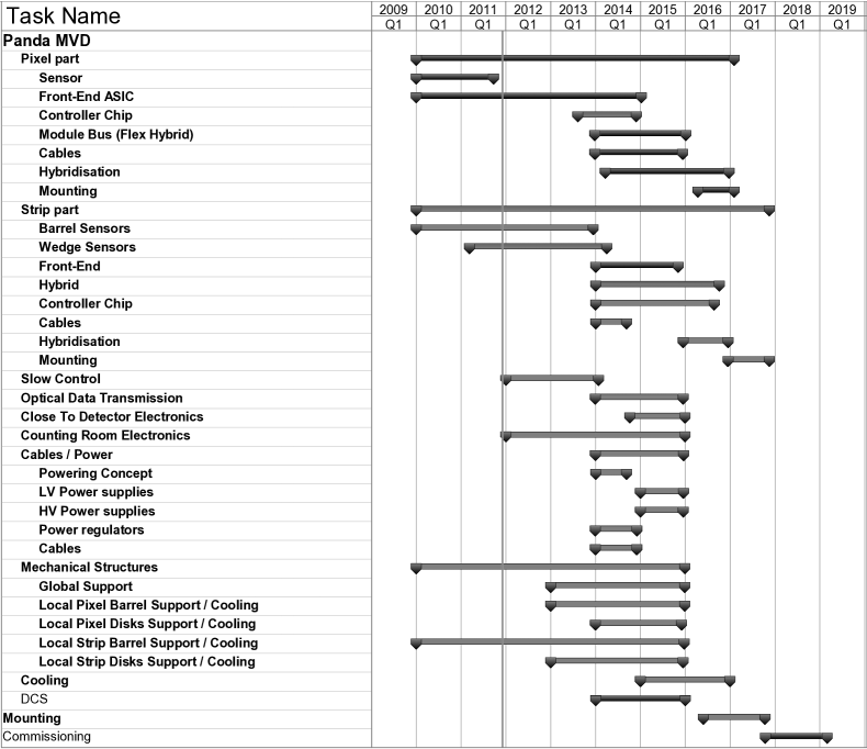
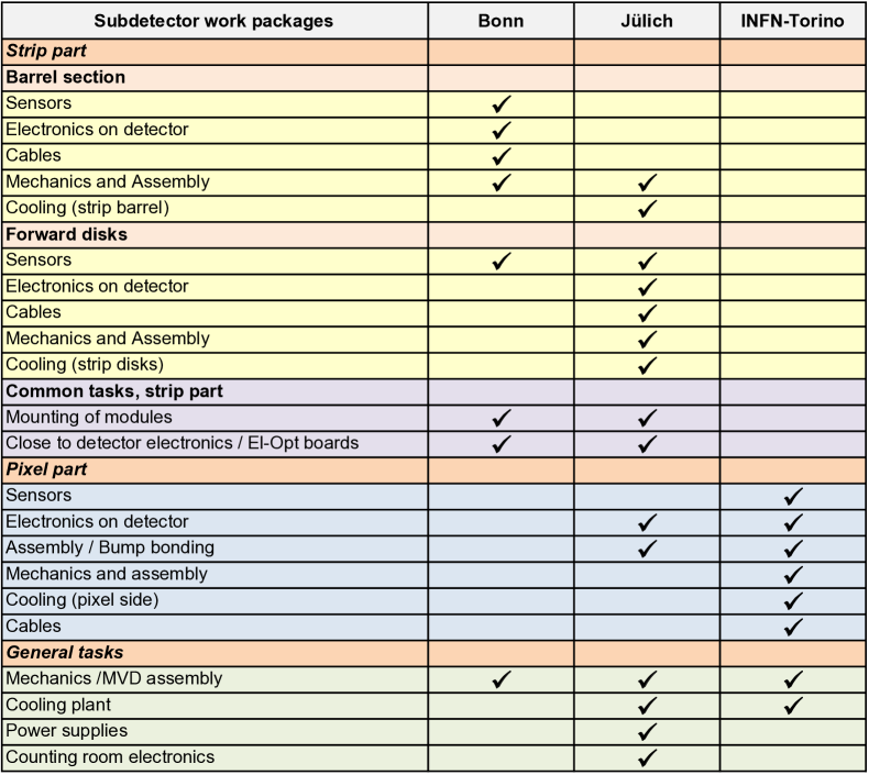
Appendix A The Bonn Tracking Station as a Validation for the Simulation Framework
A.1 The BonnTracking Station
The implementation of silicon devices such as microstrips or pixels requires suitable tools to evaluate the main features either for sensors or for connected \frontendelectronics. Among these studies those ones using a particle beam are very important. For that purpose a beam telescope based on silicon strips was designed and built by the Bonn MVD group. It consists of four boxes positioned along the beam direction covering a maximum longitudinal range of nearly 200 cm. Each box is provided with silicon strips. Single sided and double sided sensor were used. Both kinds have an active area of , a thickness of 300 m, a pitch of 50 m and a 90∘ stereo angle. Four scintillators are disposed along the beam axis: two of them before and two after the silicon sensors. They generate signals which are used for triggering the readout. The tracking station allows to change the longitudinal position of each box and provides a specific holding frame permitting rotations of the device under test, which is located in the center of the telescope. The operative setup of the tracking station is shown in figure A.1.

The tracking station has been tested in different beam conditions:
-
•
2.95 \gevcand 893 \mevcprotons at COSY (Jülich);
-
•
1 to 5 \gevelectrons at DESY (Hamburg);
-
•
Bremsstrahlung photons from an electron beam of 2 \gevat ELSA (Bonn).
-
•
lepton pair production from Bremsstrahlung photons at ELSA (Bonn).
A.1.1 Layout of the DAQ Chain
The data acquisition and reduction is done in several layers. First, all channels of the Si-Strip Sensors are time discretely sampled after amplification and pulse shaping through APV25 \frontendASICs when an external trigger is asserted. The resulting analog samples are multiplexed in a single mixed (analog and digital) output per \frontendthat is sampled by an ADC running synchronous to the \frontendclock. The ADCs are actually plug-in cards attached to universal FPGA-Modules with VME form factor (see figure A.2) [Robert_twepp]. The FPGA configuration implements the following stages:
-
•
frame decomposition
-
•
baseline compensation
-
•
pedestal tracking
-
•
hit-over-threshold assertion
-
•
cluster finding
-
•
FIFO buffering
-
•
noise statistics
-
•
slow-control interface controller
The resulting sparsified digitised cluster data is then read out via the VME-Controller through standard network link and stored to disk and processed for online monitoring.
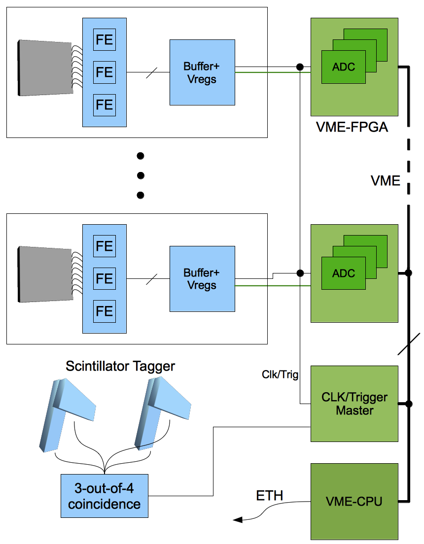
A.1.2 Structure of the Analysis Tools
The PandaRoot framework has been used to analyse the results of the measurements performed with the tracking station (see [IEEE_Bianco]). A dedicated infrastructure was required to import the DAQ raw data in the framework and there perform digitisation, hit reconstruction and analysis with the same tools usually applied to simulated data. The structure of these tools is shown in figure A.3.
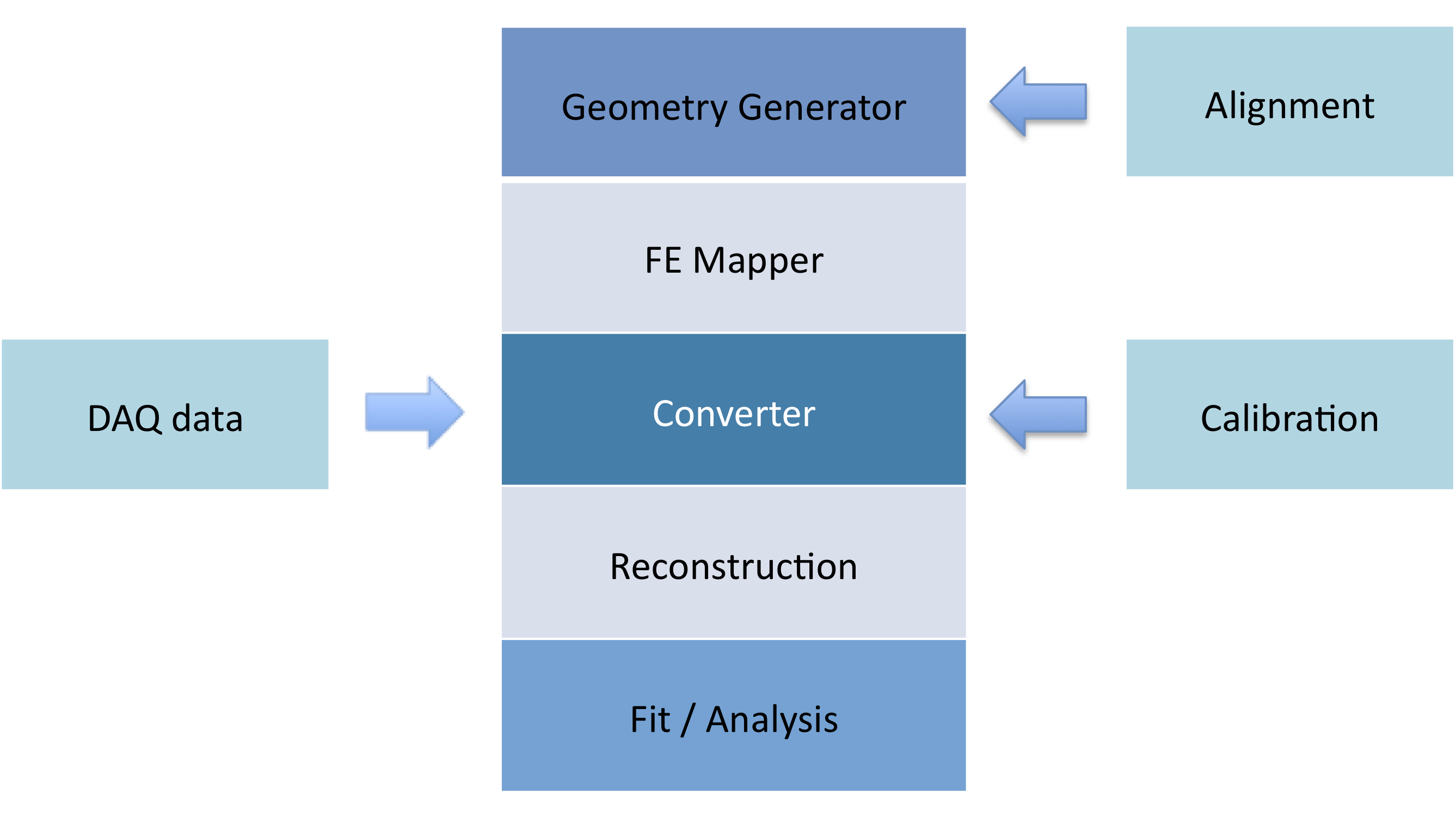
The first step toward the final analysis is the alignment. This was done in two steps: first an optical check by means of a laser pointer was performed during the installation of the modules in the beam lines. Then an iterative off-line procedure based on the residuals method was applied to measured data in order to find the real positions of the sensors. This information was inserted in the geometry definition provided to the analysis framework. A map linking \frontendchannel numbers to simulation-like strip identifiers was implemented. The calibration of the sensors envisages the energy loss measurements available with this kind of detectors. The same charge was injected on each channel of the \frontendelectronics to resolve differences in the response.
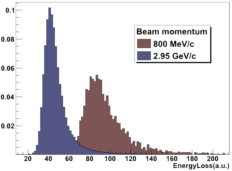
This set of tools allowed to perform clustering and hit reconstruction inside the PandaRoot simulation framework. This is a key feature to directly compare simulated and measured data, as shown in the next sections. An example of the functionality of this infrastructure is shown in figure A.4, where energy losses obtained with protons of different momenta, are compared.
A.1.3 Rotation of One Sensor
The tracking station is designed to permit the rotation of one sensor, changing in this way the incident angle of the beam to the detector plane (see figure A.5).
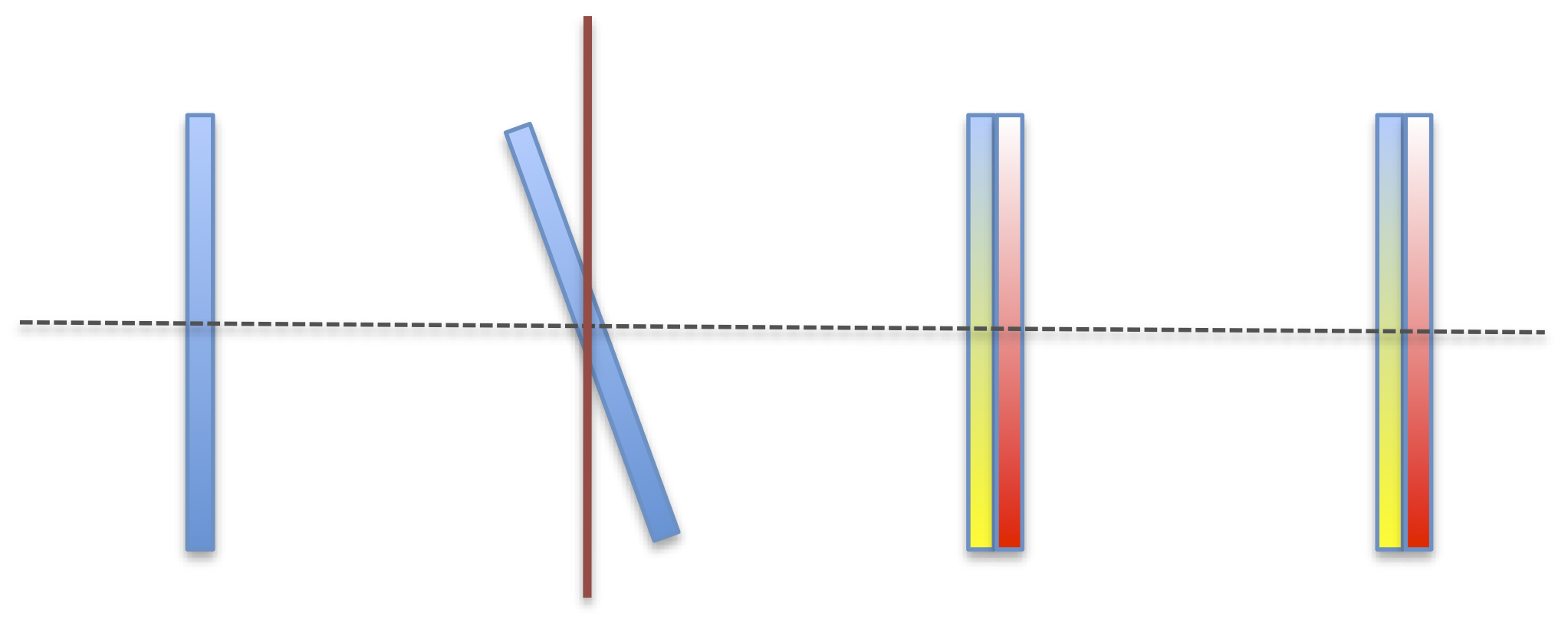
This feature is important to study the effect on cluster size and energy loss distributions. Increasing the incident angle a particle will cross the sensor along a longer path, thus having in average a bigger energy loss and hitting more strips. These effects were studied during a beam test at DESY, where 4 \gevelectrons were casted. There one of the double sided sensors was positioned on the rotating holder and several incident angles were set. As foreseen, the peak position of the energy loss distributions moves to higher values as the incident angle gets bigger (see figure A.6). A similar trend is predicted by simulations summarised in figure A.7.
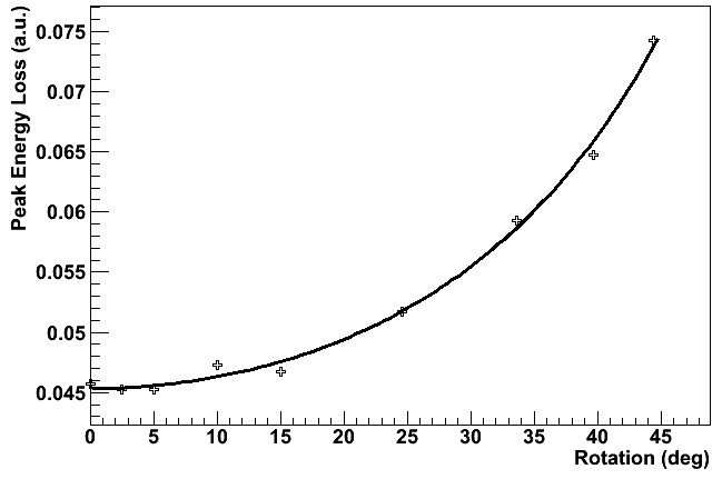
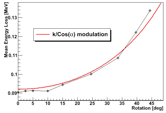
The cluster size is another variable influenced by the incident angle of the beam. Figure A.8 shows the average size of the clusters (expressed in terms of number of strips on both sides belonging to the same cluster) as a function of the rotation angle. An enhancement is present for an angle of about 9∘. Such a particular value corresponds to cross the full width of a strip, while spanning the full thickness of the sensor111.
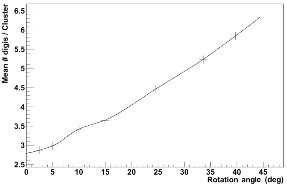
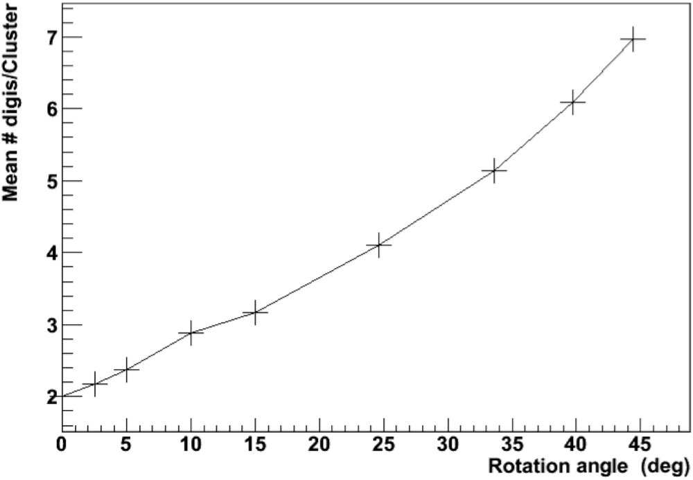
This feature is present in simulations as well, as shown in figure A.9. Simulations present some differences in the cluster sizes, although the trend is compatible with that one obtained with measured data. This is due to some thresholds set in the MC simulations, for example the minimum charge that can be collected by each strip. We could not set these thresholds according to the values observed with the real devices, since, at the moment, the absolute ADC energy loss calibration is not taken into account. Changes of these values can have a significant impact on the cluster size. A too high value for this threshold can result in a cluster with smaller multiplicity than that one obtained from measurements. On the other side too low thresholds in MC simulations can lead to bigger clusters than the measured ones, since strips where the collected charge is smaller than the hardware threshold are taken into account.
A.1.4 Shift of One Sensor
The longitudinal position of the four boxes can be modified in a wide range. One of the sensors was moved along the beam axis during a beam time with 3 \gevelectrons at DESY (see figure A.10).
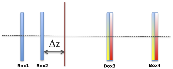
This scan was performed in order to understand the effect of the position of the second box on the tracking performance. Therefore, the unbiased resolution was extracted with different setups:
where is the standard deviation of the distribution of the x-residuals for the sensor. Results are shown in figure A.11.
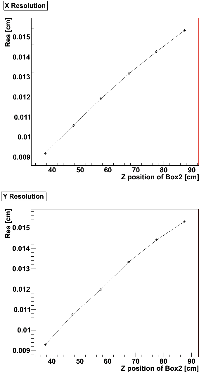
Measurements show that the best unbiased resolution is obtained when the second box is as close as possible to the first one. This means that the effect of multiple scattering in the first box is not negligible at these energies and the best condition is the one where a second point is measured before the scattering cone diverges too much from the straight trajectory.
A.1.5 Resolution Estimations
The simulation framework allows to investigate the resolutions achievable with different setups. A comparison has been realised using three different setups and a beam of 5 \gevelectrons. The simulations were performed placing and ideal silicon sensor with infinite precision at the center of the tracking station (see table A.1). This ideal sensor was set as a 300 m thick silicon volume with square area.
| B1 | B2 | Device | B3 | B4 | |
| z (cm) | z (cm) | z (cm) | z (cm) | z (cm) | |
| A | 16. | 86. | 110. | 145. | 185.5 |
| B | 90. | 100. | 110. | 120. | 130. |
| C | 65. | 85. | 110. | 139. | 159. |
The position measured by this device was compared with the one extrapolated from the tracking station hits. This last evaluation was done calculating the intersection of the straight line fitted on the tracking station points with the plane of the ideal sensor. Histograms were filled with the x and y distance between the measured and the extracted points and the distributions were fitted with Gaussians. The results are shown in table A.2.
| Setup | ||
| m | m | |
| A | 56 | 53 |
| B | 16 | 16 |
| C | 34 | 34 |
The best setup (B) is that one with all the sensors placed as close as possible to the device under study. This setup is not feasible with the actual tracking station due to some limitations of the holding structures. The setup C represents the positioning with the smallest achievable distances between the device and the tracking station boxes.
A.1.6 Scattering Measurements
The tracking station has been used to measure scattering in some volumes of different materials both with protons at COSY and with electrons at DESY. Measurements have been performed placing the scatterers on the central holder of the tracking station, with two hits measured upstream and two downstream of the volume (see figure A.12).
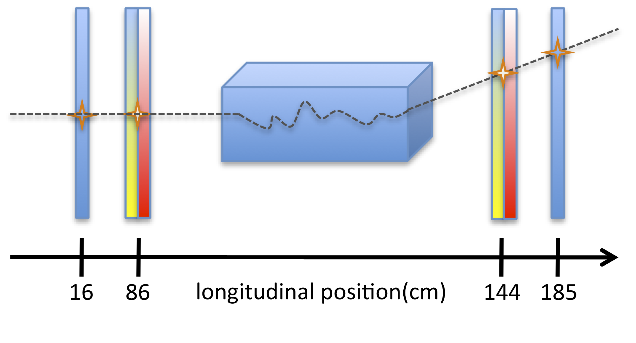
The samples used for these studies were carried out with materials foreseen in the implementation of the MVD support structures. Both carbon and carbon foams were characterised, as well as complex prototypes for the pixel staves:
-
•
empty volume: just air between the boxes;
-
•
1 cm thick carbon volume with a density of 1.79 g/cm3;
-
•
2 cm thick carbon volume with a density of 1.70 g/cm3;
-
•
2.5 cm thick of a carbon foam with a density of 0.52 g/cm3;
-
•
a 4 mm thick pixel stave prototype realised with carbon foam and embedded cooling pipes (see figure 5.30).
The analysis focused on the determination of the projected scattering distributions. For each setup the x and y projected scattering angle distributions were measured (same examples are shown in figure A.13). In their central part these distribution are well approximated by Gaussian centered around zero. In the following we will refer to and meaning the standard deviations obtained with a Gaussian fit, on the x and y projected distributions, respectively.
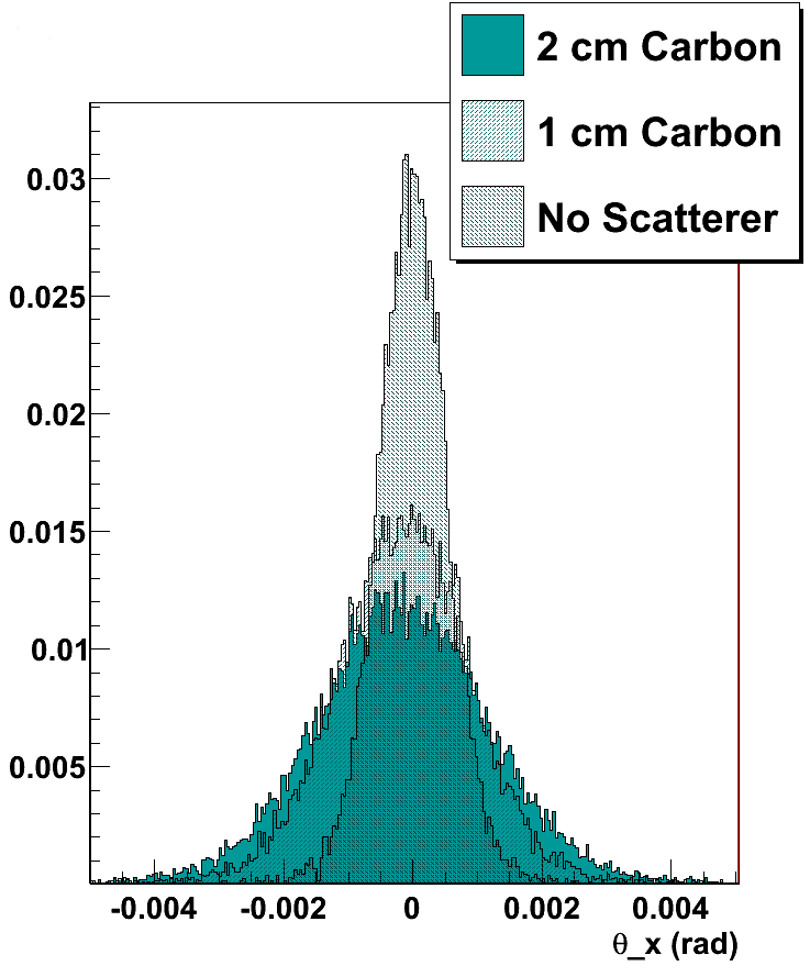
The results obtained allow to distinguish the effect of different scatterers, even with light ones. In order to validate the simulation framework as a tool for estimates of the effect of passive materials a full set of simulations has been performed. All the setups used in real measurements were reproduced allowing a direct comparison of simulations and real data. Table A.3 summarises the results obtained from measurements and simulations using different scatterers and particle beams.
| Vol. | Ptc | Mom. | Meas. | Sim. |
| \gevc | mrad | mrad | ||
| 1 cm C | p+ | 2.95 | 1.02 | 1.01 |
| 2 cm C | p+ | 2.95 | 1.34 | 1.33 |
| Air | e- | 1.0 | 1.24 | 1.40 |
| Air | e- | 3.0 | 0.423 | 0.476 |
| Air | e- | 5.4 | 0.243 | 0.284 |
| Foam | e- | 1.0 | 2.18 | 2.54 |
| Stave | e- | 1.0 | 1.76 | 1.87 |
| Stave | e- | 3.0 | 0.601 | 0.611 |
| Stave | e- | 4.0 | 0.471 | 0.483 |
Simulations are in full agreement with the measurements performed with protons. A discrepancy of the order of some 10%, between measured and simulated values, has been found for electrons, due to a stronger effect foreseen in Geant3. Anyway, the scaling of scattering with momenta and different scatterers is really well described by simulations and we can rely on the predictions of the simulation framework to evaluate the effect of passive materials.
References
Appendix B Jülich Readout System
B.1 Overview
For the development of the Micro Vertex Detector (MVD) the evaluation of prototypes and detector parts is very important. Different prototypes of the pixel \frontendchip ToPix (Torino Pixel) need to be tested and characterised under similar conditions to improve the development.
To control these devices under test (DUT) and to save the taken data a suitable readout system is necessary. To have similar conditions for different prototypes and development stages a modular concept of a readout system is required which can be adapted in a simple way to the specific interface of different types of electronics. At the same time the system must provide a high performance to allow the evaluation of single \frontendchips as well as fully assembled modules. The possibility to implement routines for online data processing is also desirable.
A digital readout system has been developed to meet all these requirements for the development of the MVD, the Jülich Readout System.
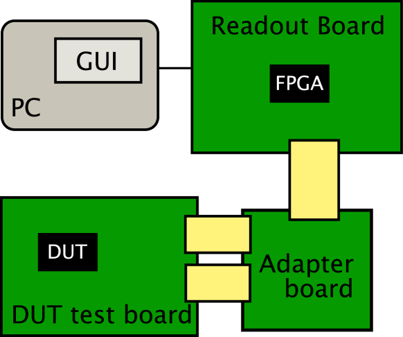
The Jülich Readout System is a compact and powerful table top setup which allows a quick testing of new detector components. The setup consists of (see figure B.1):
-
•
Digital readout board
-
•
FPGA Firmware
-
•
MRF Software with GUI
-
•
Readout PC
-
•
Device under test
-
•
Adapter board PCB
The central component is the FPGA111Field Programmable Gate Array based readout board. It is connected to the readout PC via an optical connection which is used to receive commands from the user and to send data to the PC for further processing. The corresponding software infrastructure is implemented within the MVD readout framework (MRF). The prototype is controlled by the user with a graphical user interface (GUI). On the other side the readout board is connected to the DUT on its test board. An intermediate adapter board converts the DUT signal interface to the interface of the readout board.
B.2 Basic Concepts
In the following we will outline the basic concept of the Jülich Readout System and introduce the individual components comprising the modular design.
Modularity
Complex procedures are broken down into simpler subtasks which are each handled by individual modules. To add or change functionality it is only necessary to add a new module or to change an existing one limiting required changes to individual modules which significantly improves stability and simplifies debugging. The modules can also easily be reused when already implemented subtasks reappear in a different context. This modular concept makes the readout system very flexible and easy to maintain.
Communication Layers
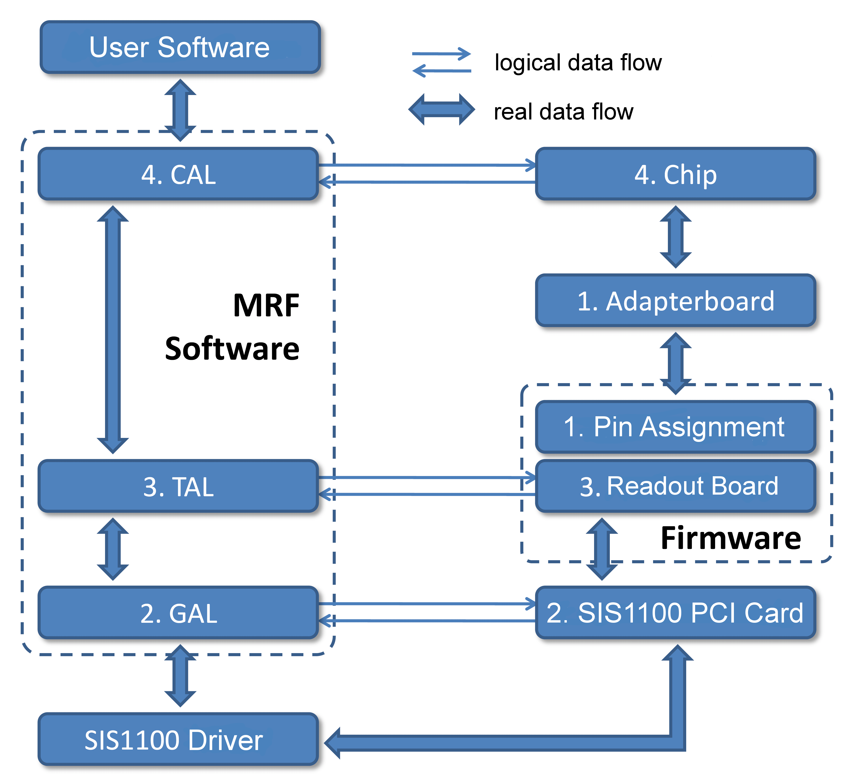
In addition to the modular setup the MRF follows the principle of different abstraction layers based on the OSI model222Open Systems Interconnection model [osi]. Following this principle, the MRF defines four communication layers (see figure B.2). Every hardware component of the readout system corresponds to a specific communication layer and has a representation in software or firmware. Each layer uses the functionality of the layer directly below, without knowledge of the exact implementation, and provides a well-defined set of functions to the layer above. Due to this approach layers can be replaced without changes to the other layers. The MRF defines the following layers:
-
•
Layer 1 - Physical Layer: Establishing of signal connections;
-
•
Layer 2 - GAL (Generic Access Layer): Communication with readout board via SIS1100 optical connection;
-
•
Layer 3 - TAL (Transport Access Layer): Access to functionality of the readout board;
-
•
Layer 4 - CAL (Chip Access Layer): Communication with DUT.
In the following, we list the most important components of the readout system and indicate to which communication layer they belong.
Adapter Board, Layer 1
The adapter board establishes the signal connection between the readout board and the DUT. Due to the usually non-standard interface of the DUT testboard, a specific adapter board needs to be developed for each type of DUT.
Digital Readout Board with Firmware, Layer 1 and 3
The FPGA based digital readout board is the main hardware component of the system. The VHDL333Very High Speed Integrated Circuit Hardware Description Language based firmware configures the FPGA with the implemented functionality (layer 3) and the pin assignment (layer 1) of the DUT interface.
Optical Connection to Readout Board, Layer 2
The data transport from the digital readout board to the PC is done via a 1 Gbit/s optical connection (SIS1100, [sis1100]). On the PC side a SIS1100 PCI card is installed. The SIS1100 interface of the digital readout board is implemented as a SIS1100 CMC (Board A) or as a combination of a SIS1100 FPGA core and an SFP444Small Form-factor Pluggable optical gigabit transceiver (Board B).
MRF Readout Software, Layer 2, 3, 4
The MRF readout software (short MRF) is the main software component of the readout system. Here the communication layers 2, 3 and 4 are defined (see chapter B.2.4). These layers establish connections to the DUT and the firmware of the digital readout board.
MRF-Control: Graphic User Interface
A graphical user interface (GUI) has been developed in C++ based on the Qt framework (see [qt]) for an easy control by the user. Full configuration and readout routines are available. Measured data can be easily saved to disk. The settings of the DUT and the setup can be saved and reload in special configuration files.
B.2.1 Digital Readout Board A
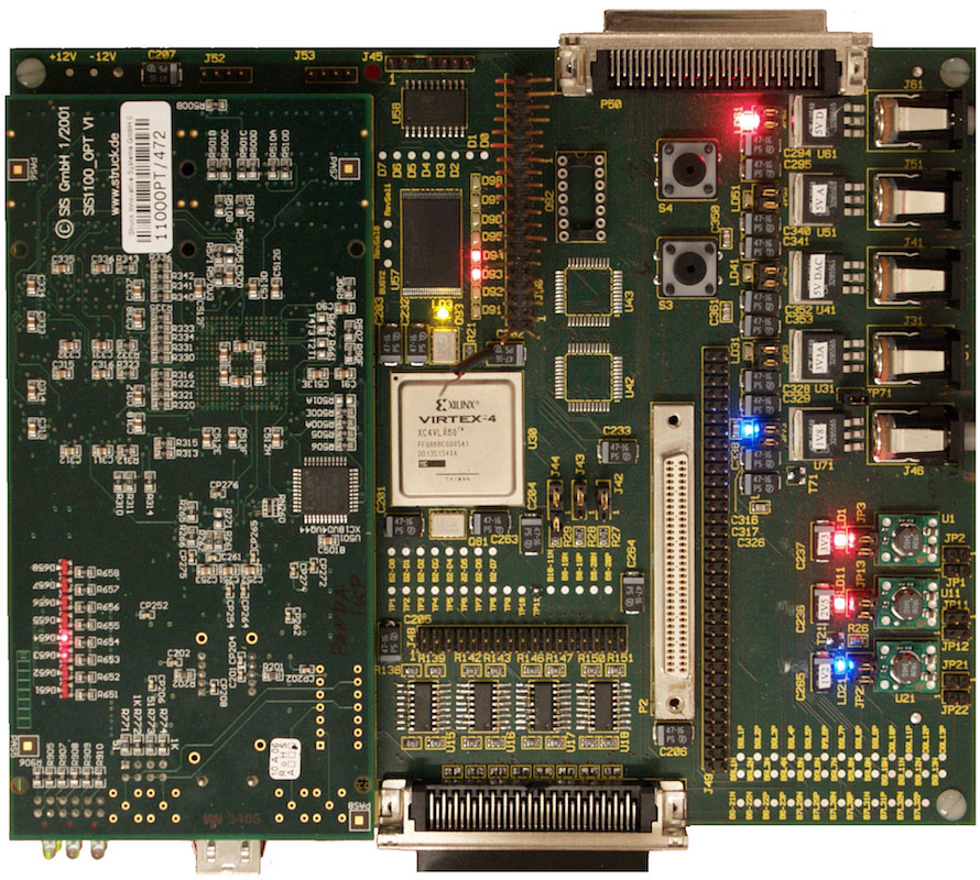
The first digital readout board (see figure B.3) is a custom development and production of the Zentrallabor für Elektronik (ZEL, Central Laboratory for Electronics) of the Forschungszentrum Jülich [development]. A Xilinx Virtex 4 FPGA, configured with the firmware, takes the control of the DUT communication and of the data buffering. The readout board is connected to the PC via a 1 GBit/s optical link. An optical fiber has the advantage of galvanic separation of PC and readout board. The SIS1100 protocol is used to transfer the data from the buffer to the PC. To implement the SIS1100 protocol on the readout board A a Common Mezzanine Card (CMC) with SIS1100 functionality is connected to the readout board. The adapter board is connected by a 68-pin flat band cable.
The main features and external interfaces of the digital readout board are:
-
•
Xilinx Virtex 4 XC4VLX60 FPGA
-
•
32 MB Xilinx Platform Flash for firmware storage
-
•
64 free configurable FPGA input/output pads
-
•
16 LVDS inputs
-
•
16 LVDS outputs
-
•
SIS1100 based optical connection to PC with 1 Gbit/s
-
•
50 MHz single ended clock
B.2.2 Digital Readout Board B
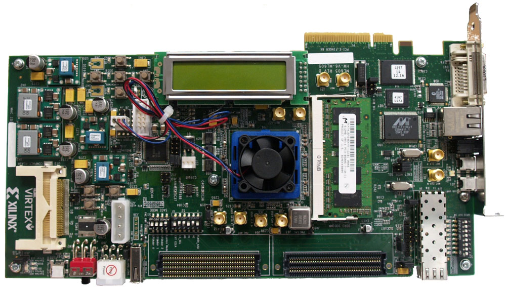
To meet the requirements of an upcoming full size ToPix prototype and online analysis an upgrade of the digital readout board was developed. The ML605 evaluation board is a commercial product by Xilinx and is comparatively cheap and easy to get. It contains a DDR3 RAM slot for data storage and a Virtex 6 FPGA (see figure B.4). The connection to the PC is established via a SFP gigabit transceiver. The SIS1100 protocol is implemented as a IP core into the firmware.
Specification of the ML605 are:
-
•
Xilinx Virtex 6 XC6VLX240T FPGA
-
•
DDR3 SODIMM memory (expandable)
-
•
SFP Module connector
-
•
FMC connectors for Standard Mezzanine Cards
-
•
LC-Display
-
•
Compact Flash Card for firmware storage
-
•
66 MHz single ended and 200 MHz differential clock
B.2.3 Firmware
The FPGA on the digital readout board is configured with a firmware which implements the desired functionality and configures the external interfaces.
The firmware for both readout boards is written in VHDL, a hardware description language, and then synthesised with the Xilinx development tools, i.e. translated to a format which is understandable by the FPGA.
The firmware is divided into modules which handle different subtask concerning the DUT, the board functionality or the communication. All modules are connected to the register manager which is itself connected to the SIS1100 interface (see figure B.5). Data which arrive via the SIS1100 are formatted in address-data pairs. The register manager will distribute the data depending on the address to the concerning modules. If data should be read from the board, the register manager will take the data from the module indicated by its address.
This modular design makes it easy to adapt the firmware to a different readout board or a different DUT respectively.
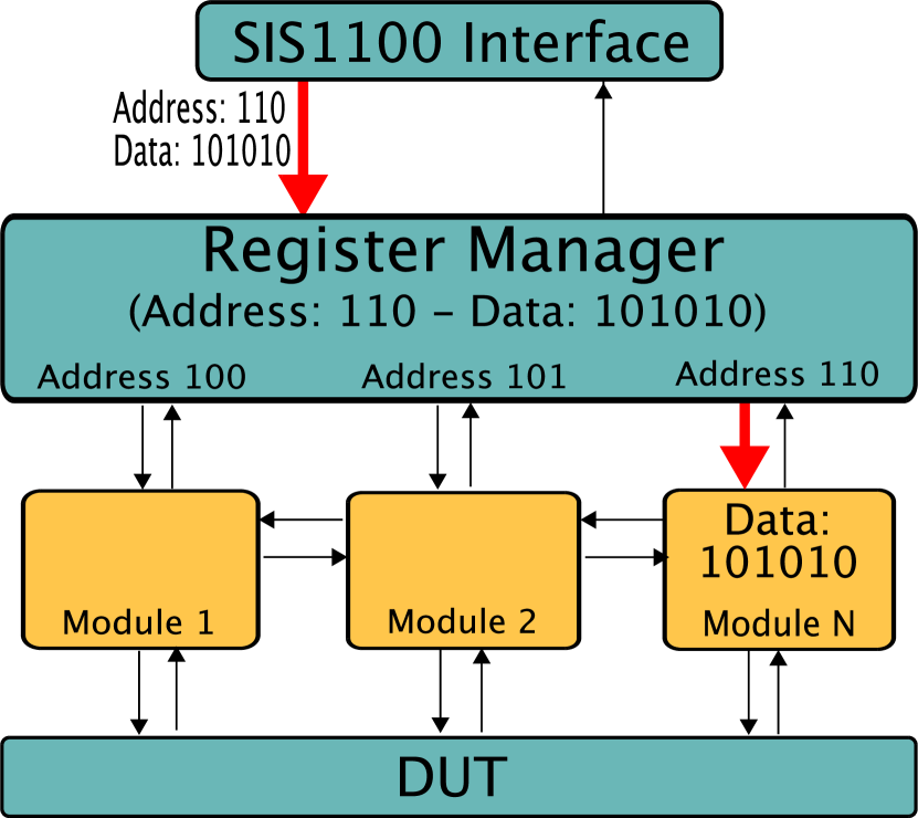
B.2.4 MVD Readout Framework
The MRF software framework implements the upper three levels of the communication model. The MRF is written in C++ and has no external dependencies except the Standard Template Library (STL) to avoid conflicts with other libraries. This makes the MRF software a decoupled package which can be used in any environment.
For every communication layer a basic set of commands is implemented to provide the data transport between the layers. In addition specific commands for the used hardware are implemented.
GAL: Generic Access Layer
The generic access layer provides the basic functionality for communication with the digital readout board. The read and write commands provide a basic reading and writing to registers over an open connection.
All more complex commands of the upper layers are implemented using these basic functions.
Including the SIS1100 driver into the GAL more powerful functionality is implemented. The SIS1100 driver provides DMA transfer555Direct Memory Access. Data from a buffer on the readout board can be send directly to a data container structure in the MRF software.
In addition the readout board is able to send interrupt signals to the PC to indicate certain conditions such as data from the DUT being available. A transfer to the PC can then be triggered automatically.
TAL: Transport Access Layer
The transport access layer provides access to the functionality of the firmware. For both versions of the digital readout board certain basic functionality is available such as the online configuration of the clock generator and the controlling of status LEDs.
CAL: Chip Access Layer
The Chip Access Layer implements the functionality of the DUT and needs to be adapted to the specific hardware e.g. configuration of the chip or the readout sequence. Two versions have been made for the control of the Atlas FE-I3 and another one for the ToPix v2. The complete readout and all testing procedures are available for both chips.
B.3 Conclusion
The Jülich Readout System has been used to test the \frontendprototypes ToPix v2 for the MVD and FE-I3 as a fallback solution. The FE-I3 has been tested with the digital readout board A, the ToPix v2 with both the readout boards A and B. Due to the modular design of the digital readout system the adaption to the different chips and hardware was very fast. Different measurements like stability tests with different clock frequencies, threshold scans and tuning of threshold dispersions have successfully been done [pohl] [thesis_mertens].
References
Appendix C Details on Vertexing
In section 6.7.2 a characterisation of the vertexing performance was shown. Four pions were propagated though the MVD volume from different common start vertices and the achieved resolutions were mapped as a function of the position of the vertex. All the scans showed a different resolution for the x and y coordinates of the reconstructed vertices. When the polar angle () of the pions reaches values at around , the vertex resolution for the x coordinate becomes worse than the y one. This is not expected because of the symmetry of the MVD design. In order to find out the reason of this effect several tests were performed. First of all the vertex finders have been characterised in detail to find out possible critical behavior. Table C.1 shows the effect of an artificial rotation of applied to tracks in the x-y plane, before applying the vertexing. This test was performed with four pions of 1 \gevcmomentum distributed over the full angular ranges ( and ). The rotation moves the worse reconstruction performance to the y coordinate, excluding a bias introduced by a different treatment of x and y by the vertexing tools.
| (m) | No Rot | |
| x | 88.3 | 69.4 |
| y | 69.4 | 88.3 |
Several investigations lead to the conclusion that this effect is due to the constrains to the design of the inner barrel layers. Because of the presence of the target pipe and due to mechanical restrictions it was impossible to cover with pixel sensors the full acceptance in the area immediately downstream of the interaction point (a schematic view is shown in figure C.1).
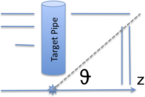
The design of barrel 1 and 2 does not foresee “forward” barrel sensors in the top and bottom regions. This translates into the fact that tracks flying into these holes in the acceptance create a smaller number of hits in the MVD and have bigger distances between their first hit and the interaction point (see figure 6.19 and figure 6.21). These particles will be reconstructed with worse performances, leading to worse vertex determination. Since these critical regions are in the top and bottom regions of the MVD, they effect much more the determination of the x coordinate of the vertex than y. This appears clearly if one propagates four pions from the interaction point, setting their angles so that they are in an orthogonal disposition in the transverse plane. There one can rotate differently the set of tracks and check the effect on vertexing performances.
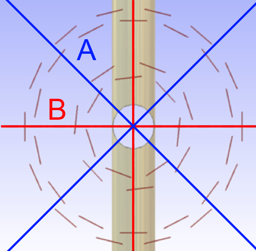
Figure C.2 shows the two configurations chosen to investigate the effect of the gaps: in case “A” the four pions do not enter the target pipe and they all create a hit in the first barrel layer, while in case “B” two tracks are propagated with initial directions pointing inside the target pipe hole. In both cases was set to for all the tracks.
| Setup | (m) | (m) |
| A cross, no pipes | 30 | 30 |
| A cross, pipes in | 33 | 33 |
| B cross, no pipes | 103 | 29 |
| B cross, pipes in | 103 | 30 |
| All , pipes in | 67 | 47 |
Table C.2 summarises the results obtained with the configurations A and B, both with and without the material of beam and target pipes defined in the geometry. It clearly appears that setup B produces a much worse vertexing performance for the x coordinate, while the configuration A shows the same behaviour for x and y. For these last studies a different vertexing tool has been used (the Kinematic Vertex Fit), to cross-check that the x-y different performances were not induced by the vertexing itself. This is the reason why results here are different from the ones obtained in the rest of this section (there the POCA method was used). The different x-y resolutions appeared to be strictly related to the polar angle of the tracks. For particles flying in the forward region the performance is the same for x and y. At of about the difference starts to appear. This can be seen in figure 6.28 where the x and y resolutions obtained with different values (integrating over the full ) are summarised.
Appendix D Alignment
D.1 Introduction
In track reconstruction and physics analysis the detector alignment is a mandatory task. An accurate determination of a large number of parameters is required to allow precise track and vertex reconstruction.
The momentum resolution of reconstructed tracks depends in part on the alignment of the detectors in space. It should not be degraded significantly (commonly 20) with respect to the resolution expected in case of the ideal geometry without misalignment.
This implies that the detectors positions must be known to an accuracy better than 20 of the intrinsic resolution. This corresponds to an alignment precision of 10 m or better in the bending plane.
Optical surveys and full mapping of MVD modules and super-modules can be a very useful starting point and a constraint in the alignment procedure but do not provide the required accuracy and cannot correct the time dependent changes of the geometry after the tracker installation. Module position fluctuations (O(10 m)) and barrel/stave/disk deformation (O(100 m)) can occurr. Therefore alignment algorithms based on the track reconstruction should be used for the determination of the sensor positions and orientations. The alignment procedure aims to determine the positions of the modules of each sub-detector. The basic problem is sketched in figure D.1.
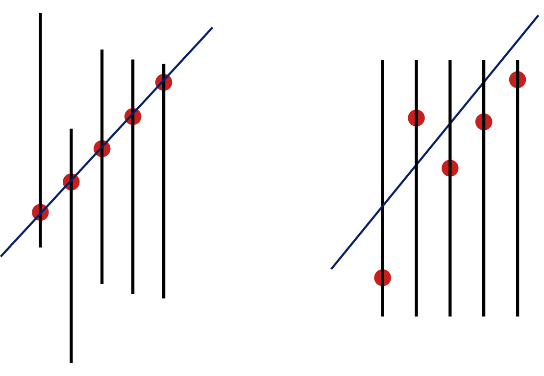
The barrels and the disks require different strategies and the last is the more difficult task. The best candidates for barrel layers alignment are cosmic rays of high momentum(p 3 \gevc) with or without magnetic field. The availability of collision track samples will be investigated in particular to align the MVD disks since they are less often traversed by cosmic ray tracks.
D.2 General Strategies and Techniques for Vertex/Tracking Detectors
Any tracking system can be considered as an assembly of separate modules, whose position can be displaced during assembling, during detector maintenance and during data taking periods as well, due to possible varying environmental conditions (temperature, humidity, elastic strains, gravitational saggings, etc.) Therefore, alignment procedures are needed to detect and correct possible distortions. Any deformation of the mechanical structure of the modules or their mislocation from the nominal position implies a depletion of the particle position determination. Therefore, mapping and recovering the position of the any tracking detector (especially the vertex ones) is of central importance to preserve the intrinsic spatial resolution of the detector during a long data taking.
The alignment of large detectors in particle physics usually requires the determination and tuning of a large number of alignment parameters, typically not smaller than 1000. Alignment parameters for instance define the space coordinates and orientation of detector components. Since they are common to all data sets of real measurements produced by the tracking system, they are called global parameters. Usually alignment parameters are corrections to default values (coming from a topological survey following the detector installation), so they are expected to be small and the value zero is their initial approximation. Alignment parameters are usually locally defined, i.e. in each module reference system.
In a three-dimensional space, the most general set of alignment parameters able to describe any displacement is constituted by 12 figures:
-
•
three rescaling of coordinate axes,
-
•
three global traslations,
-
•
three rotations,
-
•
three shearings.
The four basic types of linear displacements are shown in figure D.2.
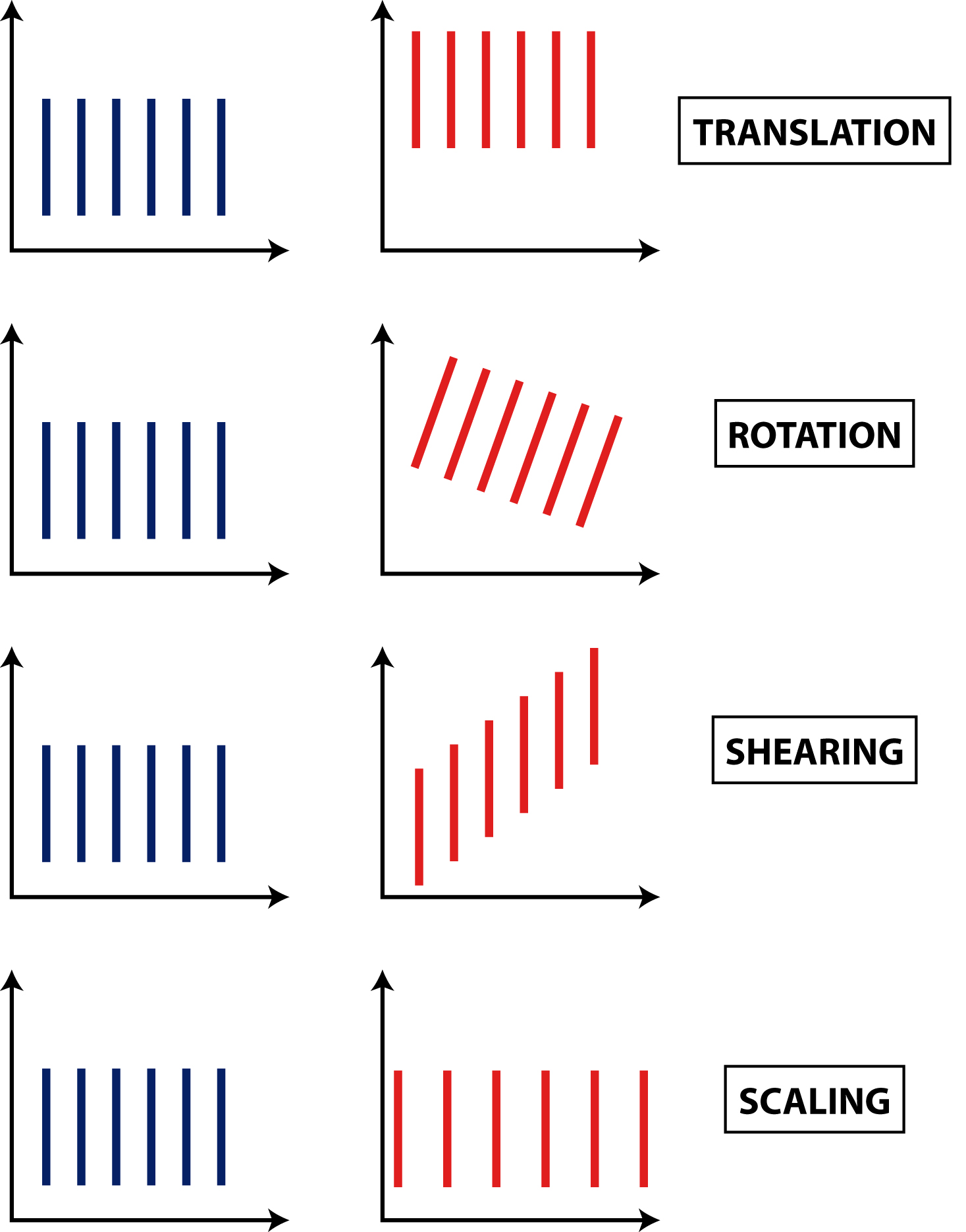
Under certain conditions some of these parameters may be fixed and the number of global parameters can be reduced. For instance, for a stack of rigid modules disposed vertically with respect to the beam axis (, as can be a stack of forward moduli), the rescaling along and , as well as a shearing, would imply a deformation of the modules and of their pitch and so these degrees of freedom can be fixed. In this particular geometrical layout, also, shearings and rotations basically coincide.
Alignment procedures are usually data-driven, so that displacements are determined comparing the measured values of hits by tracks from physics interactions and from cosmics, and fitted track coordinates. The deviations between the fitted and the measured data, the residuals, are used to determine the alignment parameters by means of proper least squares fits. Tracks are also defined through a series of parameters, which for instance describe their slopes or curvatures, and are valid for each single track only. They are called local parameters, to distinguish them from the global, alignment, ones. Despite their locality, track parameters must be defined in the global (i.e. the whole detector) reference system. Together with alignment parameters, they define the complete solution of the minimisation procedure.
In general, the alignment strategy of a stack of tracking modules proceeds through a series of stages, which can be shortly summarised as follows:
-
1.
Precision Mechanical Assembly: The modules are accurately assembled and mounted onto high precision base supports. The mounting tolerances define the scope of the possible misalignment: for instance, if a module can be placed in a box with a 20 m accuracy, one can expect misalignements to be distributed as a Gaussian centered on zero and 20 m wide.
-
2.
System Metrology: At the time of construction, coordinated measuring machines must be used to survey and fully map the surfaces of individual modules. Also mounted frames coordinates have to be fully surveyed, in standard conditions of temperature, pressure and humidity. Results from survey have then to be compared to nominal designs fixing macroscopic deviations. The outcomes from the mechanical surveys will provide the reference positions of all components.
-
3.
Software Alignment: If the quality of mechanical survey is good enough, alignment may be performed offline, during data taking or even afterwards. Otherwise, a fast alignment engine must be available to tune-up the starting alignment configuration before data taking, and possibly run whenever critical conditions are met. In general, the software alignment must be flexible enough to account for a wide range of possible occurrences arising during the data taking. Statistical methods are used to recover the actual position of the modules, as will be described in the following.
-
4.
Alignment Monitoring: A monitoring of the quality of detector alignments during data taking can sometimes be advisable; a monitoring deamon checking periodically the quality of track residuals during data taking could automatically trigger the re-running of software alignment procedures to tune online the alignment quality.
In the following, the Software Alignment stages will be described in some detail presenting the available tools commonly used in the alignment procedures of some particle physics vertex detectors.
D.2.1 Software Alignment of Tracking Modules and Modern Tools
The analysis of the residual distributions and their minimisation allow to position detector modules in their actual locations with an accuracy which is only limited by the available statistics of tracks to be fitted, and the detector intrinsic resolution.
Track residuals are functionally dependent on the both global and local parameters. The problem of alignment is in general formulated as a mathematical problem of minimisation of the functional obtained by the squares of residuals of both global and local parameters:
| (D.1) |
where is the hit residual, and the accuracy of the hit coordinate measurement. The fitted track position has as well a functional dependence both of the geometrical misalignment of the module and of the track parameters. A track model must be chosen to define the track dependence on the free parameters. For instance, in the simplest linear model, the observables have expectation values which are linearly dependent on the set of parameters. In this case, the fitted track position may be given by the linear sum of two contributions, one pertaining to the track local parameters and one to the global alignment ones, , together with their derivatives, and respectively:
| (D.2) |
Using a linear track model, the set of parameters minimising the quadratic functional is obtained solving the set of normal linear equations of least squares, in matrix form . is a symmetric matrix (), and a -vector, both of them being given by sums of independent contributions from each measurement. The solution of this system of linear equations poses the major problem of the alignment task, since the number of parameters to be determined (i.e. the dimension of the matrix of the normal equations to be inverted, to find the covariance matrix) is at least of the order of . This large parameter multiplicity requires a number of tracks to be fitted by the alignment procedure of the order of , to get a reasonable accuracy. However, this is not a severe complication as and already contain the complete information from single measurements, which thus are not needed to be stored any further. A practical limit to the number of parameters is given by the time necessary to perform the matrix inversion, which is proportional to , and to the storage/memory space (, since double precision calculations are often mandatory). This means that a number of parameters larger than starts being critical, if the matrix equation is to be solved by standard methods. With 10000 parameters, a typical computing time for matrix inversion is about six hours, which becomes almost one year for .
For the \pandaMVD, the typical number of expected degrees of freedom (for pixels stations and strips) is about 5000, about half as much as LHC experiments. Thus, at least execution times should not represent a problem.
However, the normal equation matrix could easily become singular, in case of missing data (for instance, dead channels), or in case of a complete correlation between parameters (for instance, when tracks are projected into themselves by geometrical transformations). In this case the matrix inversion fails and the analytical solution of the problem is prevented. This requires alternative approximate or iterative approaches, or special numerical algorithms to cope with the problem.
A first rough approximation is to perform a series of track fits which initially neglect alignment parameters: in this case the fits depend only on the reduced set of local parameters, and are easier to perform. However, this method is not statistically correct since the track model is basically wrong and the obtained results are biased, and possibly also unstable as affected by detector inefficiencies not taken into account. Through several iterations the method can effectively reduce the residuals (though not necessarily converging), but the alignment parameters applied as corrections in iterative fits will still be biased. Moreover, the correlations between local and global fits, present in the functional, in this way are completely ignored.
A better solution to reduce the problem dimension is to use tracks extrapolated from outer detectors, in order to fix at least the parameters of thet tracks. In this case one can align a given subdetector (for instance, stack of modules along a given axis or in a detector sector) with respect to other parts of the system. The method has the advantage of providing the alignment of the detector as a whole with high precision. On the other hand, it works effectively only when the detector dimensions are not too large, because with large extrapolation lenghts the precision of the extrapolated track parameters can soon become much worse than that for tracks reconstructed in the subdetectors only, due to multiple scattering effects and misalignements of the reference detector out of control. This is actually the method adopted for the first stage of alignment of the FINUDA vertex detector [re:finuda], composed by two layers of double-sided silicon microstrip modules (50 m pitch) arranged in cylidrical geometry around the beam axis. The applied procedure was based on a minimisation engine which aligned, by means of straight cosmic rays, stacks of four modules at a time, two per each of the two detector layers (starting from those crossed by a larger number of straight cosmic rays). Then adjacent single modules of the inner/outer layers were aligned, one at a time, with respect to the already aligned stacks. The error in the alignment of a single module, assuming multiple scattering effects are negligible, is given by the sum in quadrature of the modulus intrinsic resolution () and the alignment precision (). The minimum number of tracks needed to perform a reliable minimisation is determined by the condition . Once a satisfactory relative alignment of the two layers was achieved, they were then aligned with respect to the outer tracker (a straw tube array), which could provide information on global rotations and tilts of the vertex detector as a whole. With this method, after having taken into account multiple scattering and sagging effects, a resolution of the vertex detector moduli of about 20 m could be achieved for the coordinate, and better than 30 m for . For the sake of comparison, the starting mechanical tolerance of the holder devices was m.
The most efficient alignment method consists, of course, in making a simultaneous fit of all global and local parameters, by means of dedicated algorithms which could overtake the above mentioned matrix inversion problem. To this purpose, the MILLEPEDE II programme was developed [re:blobel0, re:blobel1, re:blobel2], and it is presently widely used for the alignment of large particle physics detectors (among them, ALICE ITS [re:aliceits], LHCb VELO [re:lhcb], HERA-B OTR [re:herab, re:herab2] and H1 SVD [re:h1]). Also FINUDA used it for fine tuning purposes). The MILLEPEDE II programme is based on partition techniques which split the problem of inversion of a large matrix into a set of smaller inversions, exploiting the feature of the matrix of being very sparse, presenting many null submatrices whose computation can be skipped reducing execution times. Depending on the fraction of vanishing submatrix elements, alignment problems with a number of global parameters of the order of 105 can be attacked with standard computing power. Of course, the matrix size ought to be conveniently reduced, whenever possible, before starting the minimisation procedure. To this purpose, some preliminary iterative steps are needed, in order to:
-
•
linearise the equations (by means of Taylor expansions), if the dependence on the global parameters happens not to be linear, and
-
•
remove outliers (i.e. data with large residuals) from the data by proper cuts (to get tighter in several iterations), of properly down-weighting them.
Sometimes the minimisation is not sufficient to achieve an optimal alignment, if some degrees of freedom are undefined, which call from additional conditions, expressed by linear (or linearised) constraints. The MILLEPEDE II programme can handle additional these linear constraints (and parameters) exploiting the Lagrange multiplier method.
The MILLEPEDE II package is originally built by two parts. The first (MILLE) is called in user programs and basically prepares the data files (containing measurements and derivatives with respect to local and global parameters, in their proper reference systems). These files are processed by the second, standalone, program (PEDE), which performs the fits and determines the global parameters, steering the solutions. The solutions for local parameters, which are track dependent, are not needed. The package, originally written in FORTRAN-77, is available for FORTRAN and C-based aligment procedures and can be easily embedded in existing alignment frameworks (AliMillePede in AliRoot, LHCb VELO alignment software package [re:velo1, re:velo2, re:velo3]).
The MILLEPEDE II package allows to achieve very satisfactory alignment conditions. Using this framework, the forward stations of the LHCb VELO detector, for instance, could be aligned with a precision of 3 m on and translational coordinates (to be compared with an intrisic resolution larger than 5 m), and with an accuracy of 0.4 mrad on the rotational degrees of freedom (around the axis). The alignment of this detector was performed using tracks from LHC pp collisions and tracks from beam halo particles crossing the whole detector. Such an approach can also be envisaged for the \pandaMVD forward disks.
References
- 3D
- 3-Dimensional
- ADC
- Analog to Digital Converter
- ALICE
- A Large Ion Collider Experiment
- ALICE ITS
- ALICE Inner Tracking System
- APV
- Analog Pipeline Voltage mode
- ASIC
- Application Specific Integrated Circuit
- ATCA
- Advanced Telecommunications Computing Architecture
- ATLAS
- A Toroidal LHC ApparatuS
- BERT
- Bit Error Rate Test
- BTeV
- B meson TeV
- CAL
- Chip Access Layer
- CCD
- Charge-Coupled Device
- CCU
- Chip Control Unit
- CERN
- Conseil Européen pour la Recherche Nucléaire
- CMC
- Common Mezzanine Card
- CMOS
- Complementary Metal Oxide Semiconductor
- CMP
- Chemical Mechanical Polishing
- CMS
- Compact Muon Solenoid
- CNT
- Counter
- COSY
- COoler SYnchrotron
- CR
- Configuration Register
- CRC
- Cyclic Redundant Check
- CRCU
- Column Readout Control Unit
- CSA
- Charge Sensitive Amplifier
- CT
- Central Tracker
- Cz
- Czochralski
- DAC
- Digital-Analog Converter
- DAFNE
- Double Annular ring For Nice Experiments
- DAQ
- Data Acquisition
- DC
- Direct Current
- DC-DC
- DC-to-DC Converter
- DCS
- Detector Control System
- DESY
- Deutsches ElektronenSYnchrotron
- DIRC
- Detector for Internally Reflected Cherenkov Light
- DMA
- Direct Memory Access
- DPM
- Dual Parton Model
- DVCS
- Deeply Virtual Compton Scattering
- ECC
- Error Correction Code
- EDM
- Electrical Discharge Machining
- EMC
- Electromagnetic Calorimeter
- ENC
- Equivalent Noise Charge
- EPICS
- Experimental Physics and Industrial Control System
- FAIR
- Facility for Antiproton and Ion Research
- FBK - ITC
- Fondazione Bruno Kessler - Istituto Trentino di Cultura
- FE
- Front-End
- FEE
- Front-End Electronics
- FEM
- Finite Element Method
- FET
- Field-Effect Transistor
- FIFO
- First In First Out
- FINUDA
- FIsica NUcleare a DAFNE
- FNAL
- Fermi National Accelerator Laboratory
- FPGA
- Field Programmable Gate Array
- FS
- Forward Spectrometer
- FTS
- Forward Tracking System
- FZ
- Floating Zone
- FZJ
- Forschungszentrum Jülich
- GAL
- Generic Access Layer
- GBLD
- GigaBit Laser Driver
- GBT
- GigaBit
- GBTX
- GigaBit Transceiver
- GBTIA
- GigaBit TransImpedance Amplifier
- GBT-SCA
- GigaBit Slow Control ASIC
- GEM
- Gas Electron Multiplier
- GR
- Guard Ring
- GSI
- Gesellschaft für Schwerionenforschnung
- GUI
- Graphical User Interface
- H1 - SVD
- H1 Silicon Vertex Detector
- HERA
- Hadron-Elektron-Ring-Anlage
- HERA-B OTR
- HERA-B Outer TRacker
- HESR
- High Energy Storage Ring
- HL
- High Luminosity (HESR operation mode)
- HR
- High Resolution (HESR operation mode)
- HR
- High Resistivity (wafers)
- HV
- High Voltage
- I2C
- Inter-Integrated Circuit
- INFN
- Istituto Nazionale di Fisica Nucleare
- IP
- Interaction Point
- ITME
- Institute of Electronic Materials Technology
- LD
- Laser Driver
- LED
- Light Emission Diode
- LENA
- Laboratorio Energia Nucleare Applicata
- LHC
- Large Hadron Collider
- LHCb
- Large Hadron Collider beauty
- LHCb VELO
- LHCb VErtex LOcator
- LNL
- Laboratori Nazionali di Legnaro
- LR
- Low Resistivity (wafers)
- LVDS
- Low-Voltage Differential Signaling
- MC
- Monte-Carlo
- MCP PMT
- Multi-Channel Plate PMT
- MDC
- Module Data Concentrator
- MDT
- Mini Drift Tubes
- MicroTCA
- Micro Telecommunications Computing Architecture
- MIP
- Minimum Ionizing Particle
- MMB
- MVD Multiplexer Board
- MOS
- Metal Oxide Semiconductor
- MPV
- Most Probable Value
- MR
- Middle Resistivity (wafers)
- MRF
- MVD Readout Framework
- MVD
- Micro Vertex Detector
- NIEL
- Non-Ionizing Energy Loss
- OSI
- Open Systems Interconnection
- PANDA
- antiProton ANnihilation at DArmstadt
- PCB
- Printed Circuit Board
- PCI
- Peripheral Component Interconnect
- PCIe
- Peripheral Component Interconnect Express
- p.d.f.
- Probability Density Function
- PD
- Photo Diode
- PDG
- Particle Data Group
- PID
- Particle Identification
- PLL
- Phase Locked Loop
- PMT
- Photomultiplier
- POCA
- Point of Closest Approach
- PRBS
- Pseudo Random Bit Sequence
- PVD
- Physical Vapour Deposition
- QCD
- Quantum Chromo Dynamics
- RF
- Radio Frequency
- RICH
- Ring Imaging Cherenkov Counter
- RMS
- Root Mean Square
- SDS
- Silicon Detector Software
- SEU
- Single Event Upset
- SFP
- Small Form-factor Pluggable
- SIMS
- Secondary Ion Mass Spectrometry
- SLHC
- Super Large Hadron Collider
- SLVS
- Scalable Low Voltage Signaling
- SMD
- Surface Mount Device
- SODA
- Synchronisation Of Data Acquisition
- SP
- Separation Power
- SR
- Shift Register
- STI
- Shallow Trench Insulation
- STT
- Straw Tube Tracker
- TAL
- Transport Access Layer
- TIA
- TransImpedance Amplifier
- TMR
- Triple Modular Redundancy
- TOF
- Time-of-Flight
- ToPix
- Torino Pixel
- ToT
- Time-over-Threshold
- TRx
- Transceiver
- TS
- Target Spectrometer
- UI
- Unit Interval
- UMC
- United Microelectronics Corporation
- UrQMD
- Ultra-relativistic Quantum Molecular Dynamic
- VCSEL
- Vertical-Cavity Surface-Emitting Laser
- VHSIC
- Very-High-Speed Integrated Circuits
- VHDL
- VHSIC Hardware Description Language
- VL
- Versatile Link
- VMC
- Virtual Monte-Carlo
- VME
- Versa Module Eurocard
- WASA
- Wide Angle Shower Apparatus
- ZEL
- Zentrallabor für Elektronik at FZJ