Large Negative Electronic Compressibility of LaAlO3-SrTiO3 Interfaces with Ultrathin LaAlO3 Layers
Abstract
A two-dimensional electron liquid is formed at the n-type interface between SrTiO3 and LaAlO3. Here we report on Kelvin probe microscopy measurements of the electronic compressibility of this electron system. The electronic compressibility is found to be negative for carrier densities of /cm2. At even smaller densities, a metal–to–insulator transition occurs. These local measurements corroborate earlier measurements of the electronic compressibility of LaAlO3-SrTiO3 interfaces obtained by measuring the capacitance of macroscopic metal-LaAlO3-SrTiO3 capacitors.
pacs:
73.20.-r, 73.40.Cg, 68.37.PsIt has been established that a two-dimensional (2D) sheet of mobile electrons is generated at the interface between the TiO2-terminated (001) surface of SrTiO3 and LaAlO3.ohtomo ; basletic ; caviglia This electron system has remarkable properties that differ significantly from the properties of 2D electron gases embedded in semiconductor heterostructures. For example, the characteristic carrier density at LaAlO3-SrTiO3 interfaces equals several /cm2, which is well above the typical densities of - /cm2 found in semiconductor heterostructures. The charge carriers at the interface originate from an electronic reconstructionnakagawa ; salluzzo and occupy Ti 3 states at the interface TiO2 layer.breitschaft For the effective mass of the electrons values in the range of 1 to 3.2 bare electron masses were reported.caviglia ; pavlenko ; shalom ; dubroka In the samples investigated the electron mobility is of order 1 000 cm2/(Vs) at 4.2 K.thiel_field Moreover the system shows coexistent superconductivity and magnetism if cooled to low temperatures.dikin ; luli_coex ; bert Furthermore, by performing capacitance measurements on SrTiO3-LaAlO3-Au and SrTiO3-LaAlO3-YBa2Cu3O7-x capacitors, a state with negative electronic compressibility was identified, where is the electrochemical potential.luli_kap In a dilute electron gas, a negative electronic compressibility results from the dominance of exchange and correlations terms, which apparently explain the negative compressibility in some semiconductor heterostructures.eisenstein_prb The origin of the observed negative compressibility of the less diluted electron liquid at LaAlO3-SrTiO3 interfaces has not been identified completely. The negative electronic compressibility of the LaAlO3-SrTiO3 interface electron system was found to exceed the negative compressibility of 2D electron gases in Si heterostructures by a factor of at least ten.kravchenko The negative electronic compressibility is also much larger than the negative compressibility recently reported in carbon nanotubes and GaAs structures.ilani ; eisenstein ; allison Although all studies of the negative electronic compressibility at LaAlO3-SrTiO3 interfaces were done with samples in which the LaAlO3 layers were 10 or 12 unit cells thick to prevent tunneling currents, which are unfavorable in capacitance measurements, the negative electronic compressibility has been predicted to occur also in samples with LaAlO3 films as thin as four monolayers, the thinnest films to generate a conducting LaAlO3-SrTiO3 interface.thiel_field Because tunneling and leakage currents through the LaAlO3 layer undermine the accuracy of measurements of the electronic compressibility using planar capacitors, we have explored such samples by local measurements of the electronic compressibility. For this we used Kelvin probe microscopy, which has previously been employed on LaAlO3-SrTiO3 heterostructures to map the distribution of the surface potential.kala With Kelvin probe microscopy it is possible to measure the electronic compressibility of samples grown without a top gate, which would be detrimental to the studies of LaAlO3-SrTiO3 heterostructures with 4 unit-cell-thick LaAlO3 layers.luli_kap ; arras ; foerg
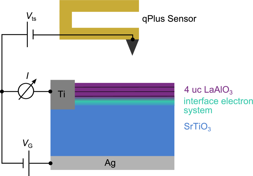
To measure the electronic compressibility of LaAlO3-SrTiO3 interfaces we fabricated LaAlO3-SrTiO3 heterostructures comprising 4 unit-cell-thick (1.6 nm) epitaxial LaAlO3 films. The LaAlO3 films were grown by pulsed laser deposition on the TiO2-terminated kawasaki ; koster (001) surface of SrTiO3 crystals. The deposition was performed at a substrate temperature of 780 °C, an oxygen background pressure of mbar, and was monitored by reflection high-energy electron diffraction. After cooling the samples in 400 mbar O2, an aluminum shadow mask with a rectangular hole was attached to the samples’ surfaces. Using this mask, Ar ion etching was employed to etch holes into the SrTiO3 substrates, which were then filled with electron-beam evaporated Ti to contact the interface electron liquid. After transporting the samples to the preparation chamber of the scanning probe microscope (SPM) they were heated radiatively for > 40 minutes to °C to clean their surfaces. The SPM, which operates in ultrahigh vacuum at 4.7 K, utilizes a cantilever based on a quartz tuning fork (qPlus-sensor) giessibl with a spring constant of N/m. An iridium spall treated in situ by field emission was used as a tip. The experimental setup is sketched in Fig. 1.
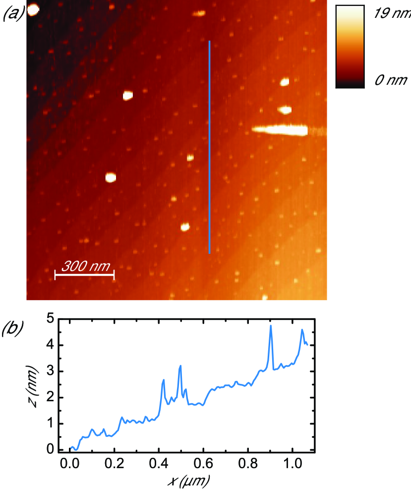
The standard step–and–terrace structure of the LaAlO3-SrTiO3 heterostructures resulting from a slight vicinal cut of the SrTiO3 substrates ( °) is readily imaged by scanning force microscopy (Fig. 2). Whereas on more standard samples excellent resolution was easily achieved with the SPM,hembacher it was not possible to obtain atomic resolution on the LaAlO3-SrTiO3 heterostructures.
To assess the electronic compressibility of the interface we measured the force between the tip and the sample as function of tip–sample distance and tip–sample voltage. The electrostatic force exerted on a tip by an electric field between the tip and a conducting sample is given by
| (1) |
where is the capacitance of the tip–sample arrangement, the tip–sample distance, and the difference of the electric potentials of tip and sample. Tip and sample are uncharged for .
If the work functions of tip and sample, and , differ, electrons move between the tip and the sample to equilibrate the electrochemical potentials of tip and sample, and . As a result, tip and sample become charged and a difference of the electric potentials of tip and sample is generated. Here, e is the elementary charge and . If in addition a voltage is applied between tip and sample, . Therefore can be determined by measuring , which is done by Kelvin probe microscopy.nonnenmacher We note that if .
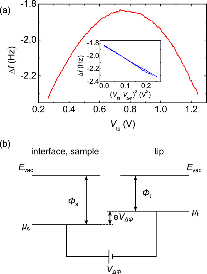
The characteristic can be determined by measuring the frequency shift of the cantilever resonance frequency as a function of , because for small oscillation amplitudes, .albrecht is the total force comprising as well as a "topographic force" , which includes forces such as van der Waals and chemical bonding forces between tip and sample. A representative spectrum of measured on a sample with 4 unit cells LaAlO3 at 4.7 K is shown in Fig. 3(a). The characteristic has a pronounced parabolic dependence (see inset of Fig. 3(a)). is given by the voltage of the parabola’s extremum. The measured sign of implies that is greater than , as is the case in the illustration shown in Fig. 3(b).
is readily obtained from the measurement of , and therefore also if is known. To measure the electronic compressibility of the interface, however, has to be measured as a function of the interface carrier density . To measure , needs to be measured at constant , while is varied by applying a gate voltage to the back of the SrTiO3 substrate. To avoid artifacts resulting from the electrostriction of the SrTiO3,schmidt for every the tip–sample distance needs to be adjusted to the same value. This is done by making use of the dependence: for every , the tip biased at is moved in -direction to obtain the same value.
The results of the measurement are shown in Fig. 4(a). Starting at , is increased if is lowered, i.e. if is lowered. At V, the slope of the curve changes sign. displays a clear minimum at V. Using a second sample and different tips, we found that this minimum was reproducible. The value of the minimum was found to differ among the samples, which we attribute to differences in the response of the samples on electric fields. The shape and the composition of the tips used in the experiments affected the absolute value of the minimum.

Because the work function of the tip does not depend on , any change of is caused by a change of , resulting from a shift of the interface chemical potential with respect to the vacuum level . A decrease of , i.e. a decrease of , corresponds to an increase of the interface chemical potential. Our data show that decreases in the voltage range from V to V. Hence in this range , the electronic compressibility is negative.bello ; tanatar
To obtain the carrier density of the interface electron system we measured the capacitance between the interface and the back gate. For this, an AC voltage with a frequency of Hz and an amplitude of mVrms was applied to the interface and the resulting current was measured with a standard lock-in technique. Because leakage currents were found to be negligibly small, the AC current is proportional to . A clear decrease in capacitance with increasing electric field is observed, which is caused by the field dependency of the dielectric constant of SrTiO3.christen The change in the carrier density with applied gate voltage can be calculated by integrating the measured capacitance. The carrier density is the sum of the density at zero gate voltage and : . The inverse compressibility can be determined by differentiating with respect to : . The result is shown in Fig. 4(b) and exhibits a clear dip of the electronic compressibility at /cm2. It is of the same order of magnitude as measured by Lu Li et al.luli_kap The absolute value differs slightly from the previously measured data, which is ascribed to the differences in the LaAlO3 film thicknesses.
In summary, we have shown with Kelvin probe microscopy that the conducting LaAlO3-SrTiO3 interface exhibits a negative electronic compressibility at low carrier densities even if the LaAlO3 layer is only four unit cells thick. This effect is consistent with the results of Lu Li et al.,luli_kap who found a negative electronic compressibility close to the metal–insulator transition for 10 and 12 unit cells LaAlO3. The employed technique is independent of the previously used capacitance-measurement method. Moreover, as we deplete the interface solely by applying voltages to the back of the SrTiO3 substrate, the use of a gate on top of the LaAlO3 film is dispensable. It is therefore possible to measure samples with ultrathin LaAlO3 films.
In Ref. kopp, it has been suggested that the capacitance of capacitors may be enhanced by optimizing the electrode material. Indeed, Lu Li et al. found a large enhancement of the capacitance of metal-LaAlO3-SrTiO3 capacitors with LaAlO3 film thicknesses of 10 and 12 unit cells.luli_kap For thinner LaAlO3 films the relative enhancement is proposed to be even larger, as the geometrical capacitance of the device is greater. Owing to tunneling and leakage currents through such thin LaAlO3 films it was not yet possible to build such devices. In view of the results reported above, we suggest to reduce the leakage currents by growing an additional dielectric layer under the top gate on heterostructures with four unit cells LaAlO3. If this additional layer has a much greater dielectric constant than LaAlO3, the geometric capacitance of the device will be reduced by only a small amount. Hence the capacitance enhancement is expected to become even greater than previously observed.
We gratefully acknowledge helpful discussions with T. Kopp, R. Jany and K. Steffen as well as financial support by the Deutsche Forschungsgemeinschaft (TRR 80) and by the European Commission (OxIDes).
References
- (1) A. Ohtomo and H. Y. Hwang, Nature 427, 423 (2004).
- (2) M. Basletic et al., Nature Mat. 7, 621 (2008).
- (3) A. D. Caviglia et al., Phys. Rev. Lett. 105, 236802 (2010).
- (4) N. Nakagawa, H. Y. Hwang, and D. A. Muller, Nat. Mat. 5, 204 (2006).
- (5) M. Salluzzo et al., Phys. Rev. Lett. 102, 166804 (2009).
- (6) M. Breitschaft et al., Phys. Rev. B 81, 153414 (2010).
- (7) G. Berner et al., k-space mapping of the Fermi surface at the LaAlO3/SrTiO3 interface: charge dichotomy, potential buildup, and O vacancies, unpublished.
- (8) M. Ben Shalom, A. Ron, A. Palevski, and Y. Dagan, Phys. Rev. Lett. 105, 206401 (2010).
- (9) A. Dubroka et al., Phys. Rev. Lett. 104, 156807 (2010).
- (10) S. Thiel et al., Science 313, 1942 (2006).
- (11) D. A. Dikin et al., Phys. Rev. Lett. 107, 056802 (2011).
- (12) Lu Li, C. Richter, J. Mannhart, and R. C. Ashoori, Nature Phys. 7, 762 (2011).
- (13) J. A. Bert et al., Nature Phys. 7, 767 (2011).
- (14) Lu Li et al., Science 332, 825 (2011).
- (15) J. P. Eisenstein, L. N. Pfeiffer, and K. W. West, Phys. Rev. B 50, 1760 (1994).
- (16) S. V. Kravchenko, V. M. Pudalov, and S. G. Semenchinsky, Phys. Lett. A 141, 71 (1989).
- (17) S. Ilani, L. A. K. Donev, M. Kindermann, and P. L. McEuen, Nature Phys. 2, 687 (2006).
- (18) J. P. Eisenstein, L. N. Pfeiffer, and K. W. West, Phys. Rev. Lett. 68, 674 (1992).
- (19) G. Allison et al., Phys. Rev. Lett. 96, 216407 (2006).
- (20) A. S. Kalabukhov et al., Phys. Rev. Lett. 103, 146101 (2009).
- (21) R. Arras, V. G. Ruiz, W. E. Pickett, and R. Pentcheva, Phys. Rev. B 85, 125404 (2012).
- (22) B. Förg, C. Richter and J. Mannhart, Appl. Phys. Lett. 100, 053506 (2012).
- (23) M. Kawasaki et al., Science 266, 1540 (1994).
- (24) G. Koster et al., Appl. Phys. Lett. 73, 2920 (1998).
- (25) F. J. Giessibl, Appl. Phys. Lett. 73, 3956 (1998).
- (26) S. Hembacher, F. J. Giessibl, and J. Mannhart, Science 305, 380 (2004).
- (27) M. Nonnenmacher, M. P. O’Boyle, and H. K. Wickramasinghe, Appl. Phys. Lett. 58, 2921 (1991).
- (28) T. R. Albrecht, P. Grütter, D. Horne, and D. Rugar, J. Appl. Phys. 69, 668 (1991).
- (29) R. G. Wilson, J. Appl. Phys. 37, 3170 (1966).
- (30) G. Schmidt and E. Hegenbarth, Phys. Stat. Sol. 3, 329 (1963).
- (31) M. S. Bello, E. I. Levin, B. I. Shklovskii, and A. L. Éfros, Zh. Eksp. Teor. Fiz. 80, 1596 (1981) [Sov. Phys. JETP 53, 822 (1981)].
- (32) B. Tanatar and D. M. Ceperley, Phys. Rev. B 39, 5005 (1989).
- (33) H.-M. Christen, J. Mannhart, E. J. Williams, and Ch. Gerber, Phys. Rev. B 49, 12095 (1994).
- (34) T. Kopp and J. Mannhart, J. Appl. Phys. 106, 064504 (2009).