Theory of Interfacial Plasmon-Phonon Scattering in Supported Graphene
Abstract
One of the factors limiting electron mobility in supported graphene is remote phonon scattering. We formulate the theory of the coupling between graphene plasmon and substrate surface polar phonon (SPP) modes, and find that it leads to the formation of interfacial plasmon-phonon (IPP) modes, from which the phenomena of dynamic anti-screening and screening of remote phonons emerge. The remote phonon-limited mobilities for SiO2, HfO2, h-BN and Al2O3 substrates are computed using our theory. We find that h-BN yields the highest peak mobility, but in the practically useful high-density range the mobility in HfO2-supported graphene is high, despite the fact that HfO2 is a high- dielectric with low-frequency modes. Our theory predicts that the strong temperature dependence of the total mobility effectively vanishes at very high carrier concentrations. The effects of polycrystallinity on IPP scattering are also discussed.
I introduction
Graphene, a single-layer of hexagonally arranged carbon atoms Novoselov et al. (2005), has been long considered a promising candidate material for post-Si CMOS technology and other nano-electronic applications on account of its excellent electrical Hwang et al. (2007) and thermal transport Balandin et al. (2008) properties. In suspended single-layer graphene (SLG), the electron mobility has been demonstrated to be as high as 200,000 cm2V-1s-1 Bolotin et al. (2008). However, in real applications such as a graphene field-effect transistor (GFET), the graphene is physically supported by an insulating dielectric substrate such as SiO2, and the carrier mobility in such supported-graphene structures is about one order of magnitude lower Bolotin et al. (2008). This reduction in carrier mobility is further exacerbated in top-gated structures in which a thin layer of a high- dielectric, such as HfO2 or Al2O3, is deposited or grown on the graphene sheet Lemme et al. (2008); Moon et al. (2010); Pezoldt et al. (2010). The degradation of the electrical transport properties is a result of exposure to environmental perturbations such as scattering by charge traps, surface roughness, and remote optical phonons which are a kind of surface excitation. Such environmental effects are encountered in metal-oxide-semiconductor (MOS) structures Fischetti et al. (2001). Hess and Vogl first suggested that remote phonons [sometimes also known as Fuchs-Kliewer (FK) Fuchs and Kliewer (1965) surface optical (SO) phonons] can have a substantial effect on the mobility of Si inversion layer carriers Hess and Vogl (1979). Fischetti and co-workers later studied the effects of remote phonon scattering in MOS structures and found that high- oxide layers have a significant effect on carrier mobility in Si Fischetti et al. (2001) and Ge O’Regan and Fischetti (2007). This method was later applied by Xiu to study remote phonon scattering in Si nanowires Xiu (2011). In Refs. Fischetti et al. (2001) and Xiu (2011) it was found that the plasmons in the channel material (Si) hybridized with the surface polar phonons (SPP) in the nearby dielectric material to form interfacial plasmon-phonon (IPP) modes. This hybridization occurrence naturally leads to the screening/anti-screening of the SPP from the dielectric material. Scattering with these IPP modes results in a further reduced channel electron mobility in 2D Si and Si nanowires.
Likewise in supported graphene, remote phonon scattering is one of the mechanisms believed to reduce the mobility of supported graphene, with the form of the scattering mechanism varying with the material properties of the dielectric substrate. Experimentally, hexagonal boron nitride (h-BN) has been found to be a promising dielectric material for graphene, and it is commonly believed that this is at least partially due to the fact that remote phonon scattering is weak with a h-BN substrate Dean et al. (2010). On other substrates such as SiO2 Chen et al. (2008); Dorgan et al. (2010) and SiC Robinson et al. (2009); Sutter (2009), the mobility of supported graphene is lower. Thus, it is important to develop an accurate understanding of remote phonon scattering in order to find an optimal choice of substrate that will minimize the degradation of carrier mobility in supported graphene.
Although the subject of remote phonon scattering in graphene Fratini and Guinea (2008); Rotkin et al. (2009); Perebeinos et al. (2008); Konar et al. (2010); Viljas and Heikkilä (2010) and carbon nanotubes Perebeinos et al. (2008); Rotkin et al. (2009)) has been broached in the recent past, the basic approach used in the aforementioned works does not deal adequately with the dynamic screening of the SPP modes. In graphene, dynamic screening of SPP modes has its origin in SPP-plasmon coupling, and the two time-dependent phenomena have to be treated within the same framework. Typically, the coupling phenomenon is ignored, and screening of the SPP modes is approximated with a Thomas-Fermi (TF) type of static screening Konar et al. (2010); Li et al. (2010); Fratini and Guinea (2008), which is adequate for the case of impurity scattering Adam et al. (2009, 2007) but can lead to a miscalculation of the scattering rates since the use of static screening underestimates the electron-phonon coupling strength Fratini and Guinea (2008), especially for higher-frequency modes. The failure to incorporate correctly SPP-plasmon coupling into the approach means that the dispersion relation of the SPP (or, more accurately, of the IPP) modes is incorrect and that the dynamic screening of the remote phonons is not accounted for in a natural manner.
To understand the screening phenomenon in our situation, let us first give a bird’s eye view of the physical picture. This picture is somewhat different from what is found in the more familiar semiconductor-inversion-layer/high--dielectric geometry, since the absence of a gap in bulk graphene renders its dielectric response stronger and qualitatively different – almost metal-like, as testified by the presence of Kohn anomalies in the phonon spectra Lazzeri and Mauri (2006); Pisana et al. (2007) – than the response of a two-dimensional electron gas. Graphene plasmons interact with the SPP modes through the time-dependent electric field generated by the latter, and the former are forced to oscillate at the frequency of the latter (). When is less than the natural frequency of the plasmon (), i.e. , the electrons can respond to the SPP mode and screen its electric field. On the other hand, when , the motion of the plasmons lags that of the SPP mode, resulting in poor or no screening, or even in anti-screening, which can actually augment the scattering field Ridley (1999). In bulk SiO2, the main TO-phonon frequencies are around 56 and 138 meV. At long wavelengths (m), the plasmon frequencies for a carrier density of are comparable or smaller than the TO-phonon frequencies. Thus, a TF-type approximation is inadequate especially for describing the screening (or more accurately, the anti-screening) of the 138 meV TO phonon modes. Our calculations suggest that, contrary to what is found in the semiconductor/high- case Fischetti et al. (2001) and to the claims made in Ref. Fratini and Guinea (2008), the higher-frequency SPP modes cannot be ignored despite their reduced Bose-Einstein occupation factors at room temperature.
It is our intention in this paper to provide a systematic description of the coupling between the substrate SPP and the graphene plasmon modes, and relate this coupling to the dynamic screening phenomenon. Our theory can be generalized to graphene heterostructure such as double-gated graphene although this falls outside the scope of our paper and will be the subject of a future work. We begin by deriving our model of the IPP system. Its dispersion is then calculated from the model. The pure SO phonon and graphene plasmon branches are compared with the IPP branches. Also, we compute the electron-IPP and the electron-SPP coupling coefficients for different substrates (SiO2, h-BN, HfO2 and Al2O3). We show that the IPP modes can be interpreted as dynamically screened SPP modes. Scattering rates are then calculated and used to compute the remote phonon-limited mobility for different substrates at room temperature (300 K) with varying carrier density. The temperature dependence of at low and high carrier densities is compared. Using the results, we analyze the suitability of the various dielectric materials for use as substrates or gate insulators in nanoelectronics applications. We also discuss the effects of polycrystallinity on remote phonon scattering.
II Model
II.1 Coupling between substrate polar phonons and graphene plasmons
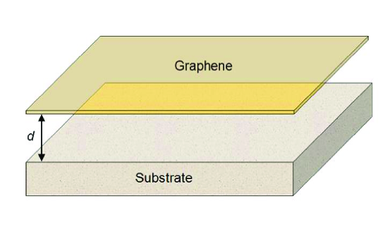
Our approach to constructing the theoretical model of the coupled plasmon-phonon systems follows closely that of Fischetti, Neumayer and Cartier Fischetti et al. (2001) although some modifications are needed to describe the plasmon-phonon coupling. One of the primary difficulties in describing the coupled system is the anisotropy in the dielectric response of graphene: graphene is polarizable in the plane but its out-of-plane response is presumably negligible. If the graphene sheet is modeled as a slab of finite thickness with a dynamic dielectric response in the in-plane direction [ where is the plasma frequency] and none in the out-of-plane direction [], the dispersion of the SPPs remains unchanged, indicating that the SPP and plasmon modes are uncoupled. This absence of coupling is implicitly assumed in much of the current literature on SPP scattering in graphene Fratini and Guinea (2008); Li et al. (2010); Konar et al. (2010); Viljas and Heikkilä (2010); Perebeinos and Avouris (2010) although it has already been shown to be untrue in 2D Si Fischetti et al. (2001) and Si nanowires Xiu (2011). Furthermore, there is considerable experimental support for the coupling of graphene plasmons to the SPPs Liu et al. (2008); Liu and Willis (2010); Fei et al. (2011); Koch et al. (2010). As we will show later, accounting for this coupling results in the formation of IPP modes which are screened/anti-screened and scatter charge carriers in graphene more weakly/strongly than the unhybridized SPP modes. This ‘uncoupling problem’ persists even when one inserts a vacuum region between the graphene slab and the substrate. Ultimately, this alleged lack of coupling can be traced back to the continuity of the electric displacement field at the interface between the graphene slab and the substrate/vacuum. Given that the dynamic response of the graphene is only in the in-plane directions and that the coupling should be with the p-polarized waves of the substrate, the slab approach is not likely to be correct. To overcome this difficulty, we find it is necessary to treat the graphene as a polarizable charge sheet (as shown in Fig. 1) rather than as a finite slab with a particular in-plane dielectric function. This polarization charge then generates a discontinuity in the electric displacement along the surface of the graphene. It is this discontinuity that couples the dielectric response of the substrate to that of the graphene sheet. The basic setup is shown in Fig. 1. The graphene is an infinitely thin sheet co-planar with the - plane and floating at a height above the substrate which occupies the semi-infinite region . Notation-wise, we try to follow Ref. Fischetti et al. (2001). In the direction perpendicular to the interface, the (ionic) dielectric response of the substrate is assumed to be due to two optical phonon modes, an approximation used in Ref. Fischetti et al. (2001), that is:
| (1) |
where and are the first and second transverse optical (TO) angular frequencies (with ), and , and are the optical, intermediate and static permittivities. We can also express in the generalized Lyddane-Sachs-Teller form:
where and are the first and second longitudinal optical angular frequencies. The variables and represent the two-dimensional wave and coordinate vector in the plane of the interface, respectively.
As in Ref. Fischetti et al. (2001), we try to derive the longitudinal electric eigenmodes of the system since the transverse modes (given by poles of the total electric response) correspond to a vanishing electric field and so to a vanishing coupling with the graphene carriers. In effect, the longitudinal modes are the transverse-magnetic (TM) solutions of Maxwell’s equations. It was also shown in Ref. Fischetti et al. (2001) that one may ignore the effects of retardation. Therefore, we need only to employ simpler electrostatics instead of the full Maxwell’s equations.
We begin our derivation by writing down the Poisson equation for the bare scalar potential ,
| (2) |
where is the (periodic) polarization charge distribution at the surface of the substrate that is the source of scattering, and is the permittivity of vacuum. Equation (2) describes the electrostatic potential within the graphene. However, the effective scalar potential felt by the graphene carriers is different and should include the collective screening effect of the induced electrons/holes, which changes the RHS of Eq. (2). Hence, we modify Eq. (2) by adding a screening charge term on its RHS, and we obtain the Poisson equation for the screened scalar potential ,
| (3) |
where is the screening charge term. The integral form of Eq. (3) is:
| (4) |
where is the Green function that satisfies the boundary conditions [see Eqs. (14d)], and the equation:
| (5) |
The bare potential is defined as . The second term on the RHS of Eq. (4) represents the screening charge distribution. The bare and screened potentials can be written as sums of their Fourier components:
| (6a) |
| (6b) |
where it must be understood that only the real part of Eq. (6b) is to be taken here and in the following sections. Given the cylindrical symmetry of the problem, the Fourier components and depend only on the magnitude of the wave vector .
From Eq. (4) we obtain the following expression for the -dependent part of the Fourier-transformed screened potential:
| (7) |
Equation (7) is solvable if the polarization charge is expressed as a function of the screened scalar potential. Here, we assume that responds linearly to , and write the screening charge term as:
| (8) |
where is the in-plane 2D polarization charge term, and governs the polarization charge distribution in the out-of-plane direction. For convenience, we model the graphene as an infinitely thin sheet of polarized charge and set . Combining Eqs. (7) and (8), we obtain the expression:
| (9) |
The expression in Eq. (9) becomes:
and the corresponding component of the electric field perpendicular to the interface at is:
| (10) |
For notational simplicity, we write:
| (11a) |
| (11b) |
where
| (12) |
Here, we emphasize that Eq. (11a) is the key to determining the dispersion relation as we shall show later.
The Green function in Eq. (7) obeys the relation:
| (13) |
We require the Green function to satisfy the following conditions at and away from the interface ().
| (14a) |
| (14b) |
| (14c) |
The bare potential in Eq. (11a) can be written as:
where and are the amplitudes of the bare potential for and respectively. Thus, the expression for the screened potential in Eq. (11a) is:
| (16) |
At the interface , the continuity of the component of the electric field parallel to the interface requires the continuity of , i.e. , giving us:
| (17) |
Similarly, the continuity of the perpendicular component of the electric displacement, i.e., leads to:
| (18) |
Substituting Eqs. (14a) and (14b) into Eqs. (17) and (18), we obtain the following relations:
| (19a) |
| (19b) |
Rearranging the terms in Eq. (19b) we obtain:
| (20) |
which can be rewritten as:
or more explicitly:
| (21) |
Equation (20) gives us the dispersion of the coupled plasmon-phonon modes, and is sometimes called the secular equation Fischetti et al. (2001). Physically, we expect three branches (two phonon and one plasmon). We write the coupled plasmon-phonon modes as , and for each -point. In the limit , Eq. (21) becomes:
which gives us as expected the dispersion for the two uncoupled SPP branches and the single plasmon branch in isolated graphene.
II.2 Plasmon and phonon content
The solutions of Eq. (21) represent excitations of the IPP modes. However, the effective scattering amplitude of a particular mode may not be substantial if it is plasmon-like. Scattering with a plasmon-like excitation does not necessarily lead to loss of momentum since the momentum is simply transferred to the constituent carriers of the plasmon excitation and there is no change in the total momentum of all the carriers. On the other hand, scattering with a phonon-like excitation does lead to a loss of momentum since phonons belong to a different set of degrees of freedom. Therefore, as in Ref. Fischetti et al. (2001), it is necessary to define the phonon content Kim et al. (1978) of each IPP mode. The phonon content quantifies the modal fraction that is phonon-like and modulates its scattering strength. Likewise, we can also define the plasmon content of the mode. To find the plasmon content, we first consider the two solutions () obtained from the secular equation Eq. (21) by ignoring the polarization response [setting ]. Following Ref. Fischetti et al. (2001), the plasmon content of the IPP mode is defined here as:
| (22) |
where the indices are cyclical. Note that the expected ‘sum rule’ Fischetti et al. (2001)
| (23) |
holds. Equation (23) implies that the total plasmon weight of the three solutions is equal to one (as it would be without hybridization). The (non-plasmon) phonon content is then defined as . In order to distinguish the phonon-1 and phonon-2 parts of the non-plasmon content, we need to define the relative individual phonon content. For phonon-1, this is accomplished by ignoring its response and replacing in Eq. (21) with . From the solutions of the modified secular equation ( and ), the relative phonon-1 content of mode will be:
| (24) |
where, as before, , and are cyclical. The relative phonon-2 content can be similarly defined by replacing the superscript with . Hence, the TO-phonon-1 content will be:
| (25) |
The TO-phonon-2 content can be similarly defined. Given Eqs. (22) and (25), the following sum rules have been numerically verified:
| (26) |
for each mode .
II.3 Scattering strength
As we have seen earlier, the IPP modes that result from the SPP-plasmon coupling have a different dispersion from that of the uncoupled SPP and plasmon modes. The electric field generated by the IPP modes is also different from that of the uncoupled SPP and plasmon modes. Since the remote phonon-electron coupling is derived from the quantization of the energy density of the electric field Fischetti et al. (2001), we expect this difference in the electric field to be reflected in the scattering strength of the IPP modes.
To find the scattering strength of an IPP mode, we have to determine the amplitude of its electric field. In Eq. (16) there are three unknowns (, and ), two of which ( and ) can only be eliminated through Eqs. (17) and (18). To find , we follow the semi-classical approach in Ref. Fischetti et al. (2001), where the time-averaged total energy of the scattering field is set equal to the zero-point energy. In the following discussion, we set We first compute the time-averaged electrostatic energy associated with the screened field:
| (27) |
The angle brackets denote time average. The volume integral in Eq. (27) is the result of three contributions: one from the substrate (), one from the graphene-substrate gap (), and one from the region above the graphene (). Each term can be converted into a surface integral. Adopting a ‘piecewise approach’ to evaluate the integral in Eq. (27), we must evaluate three surface integrals. To do so, we need the explicit expressions for :
| (28) |
and for :
| (29) |
We can now evaluate the electrostatic energy in the regions , and .
| (30) |
As mentioned earlier, the volume integrals in Eq. (27) can be recast as surface integrals. Thus,
| (31a) |
| (31b) |
| (31c) |
In Eq. (31b), is the dielectric function of the substrate, which we distinguish with the overhead bar, and distinct from . As we shall see later, as in Ref. Fischetti et al. (2001), the function is chosen in a way consistent with the particular excitation that we want. Let us regroup the terms in Eqs. (31c) into those on the substrate surface at and those on the graphene at . At , we have
| (32) |
while at , we have:
| (33) |
We have to be careful in computing . Mathematically, it may seem that we ought to set . However, note that the term accounts for the various excitation effects, ionic and electronic, but the term corresponds to the charge singularity in the zero-thickness graphene sheet. It is a ‘self-interaction’ of the charge distribution in the graphene which has no dependence on , unlike , so that we should not expect it to contribute physically to the scattering of the graphene carriers. To see this more clearly, we rewrite Eq. (27) as:
where and are the polarization fields of the lattice (substrate) and the graphene electronic excitation respectively. The following identification can be made:
and since we are only interested in the interaction of the lattice polarization field with the graphene carriers, we set , i.e.:
| (34) | |||||
where we have used the relationship . In Eq. (34), the first factor resembles the secular equation, Eq. (20). Indeed, if we replace with , then as expected. This is no coincidence since represents the energy of the charge distribution present at the substrate-vacuum interface and the secular equation in Eq. (20) is a statement about the absence of charges at the substrate-vacuum interface. This also confirms our earlier choice of excluding the contribution from the surface charges at , since that contribution does not disappear when we replace with . By regrouping the terms according to the position of their charge distribution in Eq. (30), we make the relationship to the secular equation Eq. (20) manifest. Using Eq. (12), the expression for the screened electrostatic energy can be rewritten as:
| (35) |
We use the relationship to obtain the time-averaged total energy, and set it equal to the zero-point energy, i.e., , so that:
Therefore, the squared amplitude of the field is:
To determine the strength of the scattering field, say for the TO1 phonon, we take the difference between (i) the squared amplitude of the field with the TO1 mode frozen and (ii) that of the field with the mode in full response. In (i), we set:
and
The squared amplitude of the TO1 scattering field for is:
| (36) | |||||
The expression for the TO2 scattering field can be similarly obtained. Therefore, the TO1 effective scattering field can be written as:
| (37) |
The scattering potential is:
| (38) |
where () is the annihilation (creation) operator for the mode corresponding to and . Generally, the graphene field operator can be written in the spinorial form as:
| (39) |
where denotes the valley, and the sign corresponds to the band; () is the annihilation (creation) operator of the -band electron state at the valley. Therefore, the interaction term is
and, if we neglect the inter-valley terms, simplifies to:
| (40) |
where
is the overlap integral that comes from the inner product of the spinors, and
| (41) | |||||
is the electron-phonon coupling coefficient corresponding to the mode.
II.4 Landau damping
At sufficiently short wavelengths, plasmons cease to be proper quasi-particle excitations because of Landau damping Ridley (1999). To model this phenomenon, albeit approximately, we take that to be the case when the pure graphene plasmon excitation, whose dispersion is determined by the expression , enters the intra-band single-particle excitation (SPE) continuum Hwang and Das Sarma (2007). This happens when the plasmon branch crosses the electron dispersion curve, i.e. when , and the wave vector at which this happens is . When , the electron-phonon coupling coefficient in Eq. (40) is that of Eq. (41). Although the lower-frequency IPP branches may undergo Landau damping from intra-band SPE as , we still retain them because the sum rules in Eqs. (23) and (II.2) require us to maintain charge conservation Ridley (1999). On the other hand, when , Landau damping is assumed to dominate all the IPP modes and the coupling between the substrate SPP modes and the graphene plasmons can be ignored. Instead of scattering with three IPP modes for each given wave vector, we revert to using only two SPP modes. This allows us to satisfy the sum rules in Eq. (II.2). In this case, the electron-phonon coupling coefficient in Eq. (41) can be rewritten as:
where indexes the SPP branch.
III Results and discussion
III.1 Numerical evaluation
Having set up the theoretical framework for electron-IPP interaction, we compute the dispersion of the coupled interfacial plasmon-phonon modes and study the electrical transport properties.
III.1.1 Interfacial plasmon-phonon dispersion
In this section we compute the scattering rates from the remote phonons by employing the dispersion relation () and the electron-phonon coupling coefficient (), which can be determined by solving Eqs. (20) and (40), respectively. For simplicity, to solve the latter equations we use the zero-temperature, long-wavelength approximation for Wunsch et al. (2006); Hwang and Das Sarma (2007):
| (42) |
where is the Fermi level which can be determined from the carrier density via the relation .
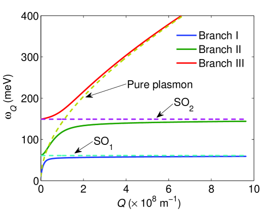
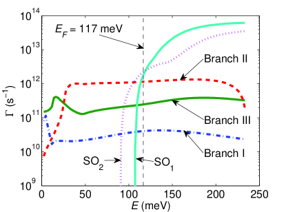
In Fig. 2 we show the dispersion relation for an SiO2 substrate with . The three coupled IPP branches are drawn with solid lines and labeled I, II and III while the dispersion of the uncoupled modes is drawn in dashed lines in the figure. The branches labeled ‘’ (61 meV) and ‘’ (149 meV) have a flat dispersion and are determined from the quantity:
while the branch labeled ‘Pure plasmon’ is determined from the zeros of the equation:
| (43) |
which gives the dispersion of the pure graphene plasmons when the frequency dependence of the substrate dielectric function is neglected and only the effect of the substrate image charges is taken into account. We observe that in the long wavelength limit (), branches I, II and III converge asymptotically to the ‘pure’ plasmon, , and branches respectively. On the other end, as , branches I, II and III converge asymptotically to the pure , and plasmon branches respectively. At intermediate values of the IPP branches are a mixture of the pure branches. The coupling between pure SO phonons and graphene plasmons has often been ignored in transport studies based on the dispersionless unscreened, decoupled SO modes Konar et al. (2010); Viljas and Heikkilä (2010); Zou et al. (2010); Fratini and Guinea (2008); Rotkin et al. (2009); Perebeinos and Avouris (2010); Li et al. (2010) On the other hand, using many-body techniques, Hwang, Sensarma and Das Sarma Hwang et al. (2010) have studied the remote phonon-plasmon coupling in supported graphene and were able to reproduce the coupled plasmon-phonon dispersion observed by Liu and Willis Liu et al. (2008); Liu and Willis (2010) in their angle-resolved electron-energy-loss spectroscopy experiments on epitaxial graphene grown on SiC. Similar results of strongly coupled plasmon-phonon modes were reported by Koch, Seyller and Schaefer Koch et al. (2010). Fei and co-workers also found evidence of this plasmon-phonon coupling in the graphene-SiO2 system in their infrared nanoscopy experiments Fei et al. (2011). Given the increasing experimental support for the hybridization of the SPPs with the graphene plasmons, it is interesting to investigate the effect of these coupled modes on carrier transport in graphene.
III.1.2 Electron-phonon coupling
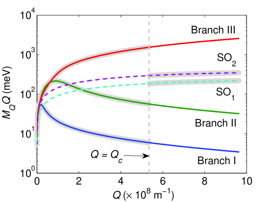
Here, the electron-phonon coupling coefficients of the IPP and the SPP modes are compared. Recall that IPP modes are formed through the hybridization of the SPP and graphene plasmon modes, and their coupling to the graphene electrons are different to that of the SPP modes. It is sometimes assumed Konar et al. (2010); Fratini and Guinea (2008) that the SPP modes are screened by the plasmons, and the IPP-electron coupling is weaker than the SPP-electron coupling. As we have discussed above, this assumption does not hold when the frequency of the IPP mode is higher than the plasmon frequency. We plot the for the SPP and IPP modes in Fig. 3.We first notice that at small , the coupling terms for branches I and II are actually larger than those for and , even though I and II are phonon-like. This is because at long wavelengths, for , resulting in anti-screening, effect which enhances the SPP electric field. For the plasmon-like branch III, is actually much larger than the those for and over the entire range of values. When we take Landau damping into account, we use the coupling coefficients (shaded in gray in Fig. 3) of branches I, II and II for and of and for .
III.2 Substrate-limited mobility
The momentum relaxation rate for an electron in band with wave vector can be written as:
| (44) |
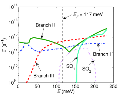
where , and . In assuming the latter expression, we use the Dirac-conical approximation. Equation (44) automatically includes the Fermi-Dirac distribution of the final states and remains applicable when the doping level is high. The individual scattering rates for the screened (I, II and III) and unscreened ( and ) branches at the carrier concentration of in SiO2 and HfO2 are plotted in Fig. 4. Landau damping is taken into account by setting the coupling coefficient of the IPP (SPP) modes to zero when (). We observe that at low energies, the IPP scattering rates are much higher than the SPP ones. At higher energies, the SPP scattering rates increase rapidly. The dominant scattering mechanism around the Fermi level appears to be due to the plasmon-like branch III in SiO2 and HfO2. In addition, at the Fermi level in , the SPP branches have scattering rates comparable to those of branch III. This explains why the low density mobility of HfO2 is less than that of SiO2.
The expression for the IPP/SPP-limited part of the electrical conductivity is:
| (45) |
where and are the spin and valley degeneracies respectively. Only the contribution from the conduction band is included in Eq. (45). We use Eqs. (44) and (45) to compute the IPP/SPP-limited electrical conductivity by setting:
| (46) |
In making this approximation, we ignore the other effects (ripples, charged impurity, acoustic phonons, optical phonons, etc). The scattering rates from the acoustic and optical phonons tend to be significantly smaller and are not the limiting factor in electrical transport in supported graphene Shishir and Ferry (2009). Impurity scattering tends to be the dominant limiting factor, but its effects can be reduced by varying fabrication conditions. Thus, the conductivity using Eq. (46) gives us its upper bound. We calculate the remote phonon-limited mobility as:
| (47) |
where is the carrier density. For in SiO2, we obtain . This is more than the corresponding values reported in the literature () Tan et al. (2007); Novoselov et al. (2005) although we have to bear in mind that it is an upper limit. Nonetheless, it suggests that IPP/SPP scattering imposes a bound on the electron mobility.
III.3 Mobility results
Although suspended graphene has an intrinsic mobility limit of at room temperature Bolotin et al. (2008), typical numbers for graphene on SiO2 tend to fall in the range 1000-20,000 Chen et al. (2008). One significant reason for this drastic reduction in mobility is believed to be the presence of charged impurities in the substrate which causes long-range Coulombic scattering Adam et al. (2007, 2009); Jang et al. (2008) and much effort has been directed towards the amelioration of the effects of these charged impurities. For example, it has been suggested that modifying the dielectric environment of the graphene, either through immersion in a high- liquid or an overlayer of high- dielectric material, can lead to a weakening of the Coulombic interaction and an increase in electron mobility Jang et al. (2008). On the other hand, actual experimental evidence in favor of this theory is ambiguous. Electrical conductivity data from Jang and co-workers Jang et al. (2008) as well as Ponomarenko and co-workers Ponomarenko et al. (2009) indicate a smaller-than-expected increase in mobility when a liquid overlayer is used. This suggests that mechanisms other than long and short-range impurity scattering are at play here. Here, we turn to the problem of scattering by IPP modes.
III.3.1 Comparing different substrates
Having set up the theoretical framework in the earlier sections, we now apply it to the study of the remote phonon-limited mobility of four commonly-used substrates: SiO2, HfO2, h-BN and Al2O3. Silicon dioxide is the most common substrate material while HfO2 and Al2O3 are high- dielectrics commonly used as top gate oxides Zou et al. (2010); Garces et al. (2011). Hexagonal boron nitride shows much promise as both a substrate and a top gate dielectric material Dean et al. (2010). The study of the remote phonon-limited mobility in these substrates allows us to understand how electronic transport in supported graphene depends on the frequencies and relative permittivities of the substrate phonons.
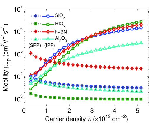
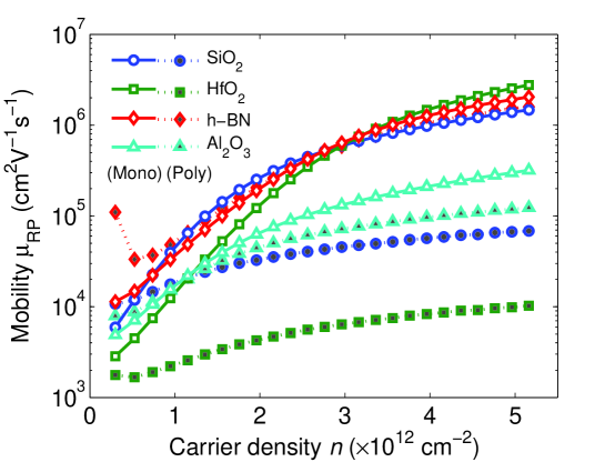
From Eq. (45) with the effects of Landau damping taken into account, we compute the remote phonon-limited mobility numerically, using the well-known Gilat-Raubenheimer method Gilat and Raubenheimer (1966) to discretize the sum in Eq. (45). We plot as a function of carrier density ( to ) at 300 K in Fig. 5. Note that the mobility values of the high- substrates (HfO2 and Al2O3) are substantially lower compared to SiO2 and h-BN in the carrier density range . Similar results have been found in MOS systems Fischetti et al. (2001). Hexagonal BN has the highest mobility at low carrier densities because of its high phonon frequencies, which corresponds to low Bose-Einstein occupancy, as well as its weak dipole coupling to graphene. In general, for all four substrates increases with because the dynamic screening effect becomes stronger at higher carrier densities. At low carrier densities, the mobility is low for all the substrates because there is a large proportion of plasmons modes whose frequencies are lower than the SPP mode frequencies. Thus, their coupling to the SPP modes results in the formation of anti-screened IPP modes that couple more strongly to the carriers, a phenomenon that has been studied for polar semiconductors Ridley (1999). However, as increases, the mobility for all four substrates rises because the plasmon frequency scales as , resulting in higher-frequency plasmon modes. Thus, the plasmon-phonon coupling forms screened IPP modes that are weakly coupled to the carriers. Furthermore, at higher carrier densities, Landau damping becomes less important as a result of the increasing magnitude of the plasmon wave vector . Contrary to expectation, we find that the mobility for HfO2 exceeds those of other substrates at larger densities (). At , HfO2 has the highest remote-phonon mobility followed by h-BN, SiO2 and Al2O3. This is because the proportion of screened IPP modes increases with increasing carrier density. Given the small values of and for HfO2, its coupling coefficients are smaller as a result of stronger dynamic screening. This weaker coupling compensates in part the higher occupation factors. In contrast, the larger values of and for h-BN imply that screening does not play a significant role at low carrier densities. Hence, its coupling to the graphene carriers does not diminish as rapidly as carrier density increases. The computed values for and h-BN highlight the role of low-frequency excitations in carrier scattering. The low-frequency modes are highly occupied at room temperature and induce carrier significant scattering at low . At higher when dynamic screening becomes important, the low-frequency modes are more strongly screened and their coupling to the carriers becomes diminished more rapidly than that of high-frequency modes.
III.3.2 Dynamic screening effects
To compute the mobility for the case without any screening or anti-screening effects, the Landau damping cutoff wave vector is decreased, i.e., , resulting in the replacement of all the IPP modes with SPP modes. We plot the SPP-limited mobility as a function of carrier density in Fig. 5 (solid symbols), and compare these results for the IPP-limited mobility. The SPP-limited mobility for different substrates spans a range of values varying over nearly two orders of magnitude. In the absence of dynamic screening or anti-screening, the SPP-limited mobility for HfO2 is only around at , more than an order of magnitude smaller than the corresponding IPP-limited mobility, because of its low phonon frequencies. This result is also clearly inconsistent with experimental observations, since significantly higher mobility values have been reported for HfO2-covered graphene Fallahazad et al. (2010); Zou et al. (2010). The drastic reduction of the computed mobility suggests that screening is very important for the determination of scattering rates in a coupled plasmon-phonon system with low frequency modes. In contrast, h-BN gives an SPP-limited mobility of at , which is still close to the IPP-limited mobility, indicating that its high frequency modes are relatively unaffected by screening. The maximum SPP-limited mobility for Al2O3 is around at , which is much smaller than the extracted by Jandhyala and co-workers Jandhyala et al. (2012) who used Al2O3 for their top gate dielectric. This disagreement reinforces the necessity of including dynamic screening effects. Furthermore, the carrier density dependence of SPP-limited mobility is different from that of IPP-limited mobility. The IPP-limited increases rapidly with carrier density because dynamic screening becomes stronger at higher , an effect that is not found in SPP-limited mobility. In contrast, SPP-limited decreases monotonically with increasing .
Our results suggest that HfO2 remains a promising candidate material for integration with graphene since its high static permittivity can reduce the effect of charged impurities Konar et al. (2010) while its IPP scattering rates are relatively low when the carrier density is high. Although its surface excitations are low-frequency, which results in high Bose-Einstein occupancy, this is offset by its relatively strong dynamic screening at higher carrier densities. Thus, IPP scattering does not represent a problem for its integration with graphene field-effect transistors. As expected, h-BN is also a good dielectric material since its high phonon frequencies imply a low Bose-Einstein occupation factor. Furthermore, its smooth interface results in a smaller interface charge density and is less likely to induce mobility-limiting ripples in graphene.
| h-BN | ||||
|---|---|---|---|---|
| () | 3.90 | 5.09 | 22.00 | 12.35 |
| () | 3.05 | 4.57 | 6.58 | 7.27 |
| () | 2.50 | 4.10 | 5.03 | 3.20 |
| (meV) | 55.60 | 97.40 | 12.40 | 48.18 |
| (meV) | 138.10 | 187.90 | 48.35 | 71.41 |
III.3.3 Temperature dependence
Remote phonon scattering exhibits a strong temperature dependence – stronger than for ionized impurity scattering – because the Bose-Einstein occupation of the remote phonons decreases with lower temperature. This change in the distribution of the remote phonons (IPP or SPP) necessarily implies that the electronic transport character of the SLG must change with temperature. At lower temperatures, scattering with the remote phonons decreases, resulting in a higher remote phonon-limited electrical mobility. The dependence of the change in mobility with temperature is related to the dispersion of the remote phonons and their coupling to the graphene electrons. By measuring the dependence of the mobility or conductivity with respect to temperature, it is possible to determine the dominant scattering mechanisms in the supported graphene. Given that our model of electron-IPP scattering differs from the more common electron-SPP scattering model, comparing the temperature dependence of the substrate-limited mobility can enable us to distinguish between the two models.
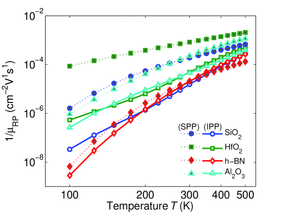
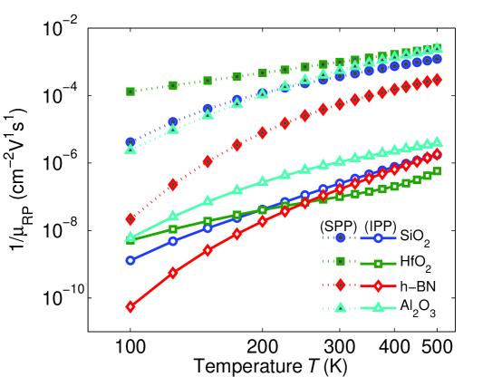
The mobility of supported graphene over the temperature range of 100 to 500 K for the different substrates is computed at carrier densities of and . For the purpose of comparison, we perform the calculation for the case with screening (IPP) and without screening (SPP). The results ( vs. ) are shown in Fig. 6a and b. In Fig. 6a, we plot the IPP- and SPP-limited inverse mobility at . As expected, the substrate-limited mobility decreases with rising temperatures for both the screened and unscreened cases. From the plots, we observe that there exists an ‘activation’ temperature for each substrate at which the inverse mobility increases precipitously. For SiO2, that temperature is around 200 K in the screened case and around 120 K in the unscreened case. This difference is striking and may be used to distinguish the IPP model from the SPP model at low carrier densities. In all four substrates, the slope of with respect to is also steeper in the IPP-limited case than in the SPP-limited case. In Fig. 6b, we plot again the IPP- and SPP-limited inverse mobility but at a much higher carrier density of . The IPP-limited is about three orders of magnitude smaller than the SPP-limited from 100 to 500 K. At high carrier densities, IPP scattering is insignificant and any changes in total mobility with respect to temperature cannot attribute to IPP scattering.
The results in Fig. 6 suggest that if IPP modes are the surface excitations that limit carrier transport in SiO2-supported graphene at room temperature, then the mobility would have a significant increase at around 200 K for . However, this IPP temperature dependence disappears at much higher carrier densities () because the IPP coupling to electrons becomes so weak that it no longer contributes significantly to carrier scattering. The results in Fig. 6 also shows that the increases monotonically with . This should be contrasted with the result of Fratini and Guinea Fratini and Guinea (2008) who found that decreases as at room temperature. This is because the coupling coefficient , which is proportional to the matrix element, scales as in the SPP model with static screening. In Fig. 3, decreases with , implying that scales as where . In other words, the coupling coefficient vanishes more rapidly with in the IPP model than the SPP model. Our results parallel those in Ref. Ren et al. (2003) in which the remote phonon-limited mobility increases with the carrier mobility in a 2-dimensional electron gas system in the Si inversion layer with high- insulators.
In supported SLG, the carrier mobility is limited by three scattering mechanisms: long-range charged impurity, short-range defect and remote phonon scattering Zhu et al. (2009). The intrinsic phonon scattering processes in graphene can be effectively neglected. Of the three scattering mechanisms, only remote phonon scattering is strongly temperature dependent. The IPP model suggests that remote phonon scattering diminishes with increasing carrier density. Thus, the experimental consequence is that the temperature dependence of the mobility in supported-SLG should weaken at higher carrier densities. On the other hand, the SPP model predicts that the temperature dependence of the mobility should increase at higher carrier densities Fratini and Guinea (2008). This difference in the temperature dependence of the total mobility between the two models should be easily discriminable in experiments.
III.3.4 Disordered graphene
We discuss qualitatively the interfacial plasmon-phonon phenomenon in disordered graphene. It is well-known that graphene grown by chemical vapor deposition (CVD) Li et al. (2009) is generally polycrystalline and contains a high density of defects. In supported graphene, charged impurities from the substrate and other defects scatter graphene carriers. These defects can affect the dynamics of plasmons in graphene which may in turn affect the hybridization between the plasmon and the SPP modes. At short wavelengths, the plasmon lifetime rapidly decreases as a result of Landau damping which results in the decay of the plasmons into single-particle excitations. At long wavelengths, the plasmon lifetime can be affected by defects in the graphene. As far as we know, there is no theory of graphene plasmon damping from defects. However, it has been pointed out that long-wavelength plasmons in polycrystalline metal undergo anomalously large damping due to scattering with structural defects Krishan and Ritchie (1970). If this is also true in polycrystalline or defective graphene, then it implies that the long-wavelength surface excitation in supported graphene are SPP, not IPP, modes.
To model phenomenologically this damping of long-wavelength plasmon modes in polycrystalline graphene with defects, we set another cutoff wave vector below which the surface excitations are SPP and not IPP modes. is possibly related to the length scale of the inhomogeneities or defects in graphene. As a guess, we choose = 6 nm, which is a typical autocorrelation length of ‘puddles’ in neutral supported grapheneAdam et al. (2011), and set . Hence, in our model, for and , the surface excitations are SPP modes while for , they are IPP modes. We compute the remote phonon-limited mobility at 300 K and plot the results in Fig. 7. We find that the long-wavelength SPP dramatically alters the carrier dependence of in SiO2, HfO2 and Al2O3. In perfect monocrystalline graphene, reaches in HfO2 and SiO2 at . On the other hand, in polycrystalline graphene with defects, it drops to the range of to . For h-BN, is quite relatively unaffected by the long-wavelength SPP modes except at low carrier densities ().
This change in remote phonon-limited mobility highlights the possible role of defects in the surface excitations of supported graphene. We emphasize that our treatment is purely phenomenological and a more rigorous treatment of plasmon damping is needed in order to obtain a more quantitatively accurate model. Nevertheless, it emphasizes the relationship between dynamic screening and plasmons. In highly defective graphene, the surface excitations may be unscreened SPPs rather than IPPs because of plasmon damping. This should be taken into account when interpreting electronic transport experimental data of exfoliated and CVD-grown graphene.
IV Conclusion
We have studied coupled interfacial plasmon-phonon excitations in supported graphene. The coupling between the pure graphene plasmon and the surface polar phonon modes of the substrates results in the formation of the IPP modes, and this coupling is responsible for the screening and anti-screening of the IPP modes. Accounting for these modes, we calculate the room temperature scattering rates and substate-limited mobility for , , h-BN and at different carrier densities. The results suggest that, despite being a high- oxide with low frequency modes, exhibits a substrate-limited mobility comparable to that of h-BN at high carrier densities. We attribute this to the dynamic screening of the low-frequency modes. The disadvantage of the higher Bose-Einstein occupation of these low-frequency modes is offset by the stronger dynamic screening which suppresses the electron-IPP coupling. Our study also indicates that the contribution to scattering by high-frequency substrate phonon modes cannot be neglected because of they are less weakly screened by the graphene plasmons. The temperature dependence of the remote phonon-limited mobility is also calculated within out theory. Its change with temperature is different at low and high carrier densities. We find that in the IPP model, the temperature dependence of the mobility diminishes with increasing carrier density only, in direct contrast to the predictions of the more commonly used SPP models. The implications of the damping of long-wavelength plasmons have also been studied. We find that the it leads to a substantial reduction in the remote phonon-limited mobility in SiO2, HfO2 and Al2O3.
We gratefully acknowledge the support provided by Texas Instruments, the Semiconductor Research Corporation (SRC), the Microelectronics Advanced Research Corporation (MARCO), the Focus Center Research Project (FCRP) for Materials, Structures and Devices (MSD), and Samsung Electronics Ltd. We also like to thank David K. Ferry (Arizona State University), Eric Pop (University of Illinois), and Andrey Serov (University of Illinois) for engaging in valuable technical discussions.
References
- Novoselov et al. (2005) K. Novoselov, A. Geim, S. Morozov, D. Jiang, M. Grigorieva, S. Dubonos, and A. Firsov, Nature 438, 197 (2005).
- Hwang et al. (2007) E. H. Hwang, S. Adam, and S. Das Sarma, Phys. Rev. Lett. 98, 186806 (2007).
- Balandin et al. (2008) A. Balandin, S. Ghosh, W. Bao, I. Calizo, D. Teweldebrhan, F. Miao, and C. Lau, Nano Lett. 8, 902 (2008).
- Bolotin et al. (2008) K. Bolotin, K. Sikes, Z. Jiang, M. Klima, G. Fudenberg, J. Hone, P. Kim, and H. Stormer, Solid State Commun. 146, 351 (2008).
- Lemme et al. (2008) M. Lemme, T. Echtermeyer, M. Baus, B. Szafranek, J. Bolten, M. Schmidt, T. Wahlbrink, and H. Kurz, Solid-State Electron. 52, 514 (2008).
- Moon et al. (2010) J. Moon, D. Curtis, S. Bui, M. Hu, D. Gaskill, J. Tedesco, P. Asbeck, G. Jernigan, B. VanMil, R. Myers-Ward, et al., Electron Device Letters, IEEE 31, 260 (2010).
- Pezoldt et al. (2010) J. Pezoldt, C. Hummel, A. Hanisch, I. Hotovy, M. Kadlecikova, and F. Schwierz, Phys. Status Solidi C 7, 390 (2010).
- Fischetti et al. (2001) M. V. Fischetti, D. A. Neumayer, and E. A. Cartier, J. Appl. Phys. 90, 4587 (2001).
- Fuchs and Kliewer (1965) R. Fuchs and K. L. Kliewer, Phys. Rev. 140, A2076 (1965).
- Hess and Vogl (1979) K. Hess and P. Vogl, Solid State Commun. 30, 797 (1979).
- O’Regan and Fischetti (2007) T. O’Regan and M. Fischetti, J. Comput. Electron. 6, 81 (2007).
- Xiu (2011) K. Xiu, in Simulation of Semiconductor Processes and Devices (SISPAD), 2011 International Conference on (IEEE, 2011) pp. 35–38.
- Dean et al. (2010) C. Dean, A. Young, I. Meric, C. Lee, L. Wang, S. Sorgenfrei, K. Watanabe, T. Taniguchi, P. Kim, K. Shepard, et al., Nature Nanotechnology 5, 722 (2010).
- Chen et al. (2008) J. Chen, C. Jang, S. Xiao, M. Ishigami, and M. Fuhrer, Nature Nanotechnology 3, 206 (2008).
- Dorgan et al. (2010) V. E. Dorgan, M.-H. Bae, and E. Pop, Appl. Phys. Lett. 97, 082112 (2010).
- Robinson et al. (2009) J. Robinson, M. Wetherington, J. Tedesco, P. Campbell, X. Weng, J. Stitt, M. Fanton, E. Frantz, D. Snyder, B. VanMil, et al., Nano Lett. 9, 2873 (2009).
- Sutter (2009) P. Sutter, Nature Materials 8, 171 (2009).
- Fratini and Guinea (2008) S. Fratini and F. Guinea, Phys. Rev. B 77, 195415 (2008).
- Rotkin et al. (2009) S. Rotkin, V. Perebeinos, A. Petrov, and P. Avouris, Nano Lett. 9, 1850 (2009).
- Perebeinos et al. (2008) V. Perebeinos, S. Rotkin, A. Petrov, and P. Avouris, Nano Lett. 9, 312 (2008).
- Konar et al. (2010) A. Konar, T. Fang, and D. Jena, Phys. Rev. B 82, 115452 (2010).
- Viljas and Heikkilä (2010) J. Viljas and T. Heikkilä, Phys. Rev. B 81, 245404 (2010).
- Li et al. (2010) X. Li, E. Barry, J. Zavada, M. Nardelli, and K. Kim, Appl. Phys. Lett. 97, 232105 (2010).
- Adam et al. (2009) S. Adam, E. Hwang, E. Rossi, and S. Das Sarma, Solid State Commun. 149, 1072 (2009).
- Adam et al. (2007) S. Adam, E. H. Hwang, V. M. Galitski, and S. Das Sarma, Proc. Natl. Acad. Sci. 104, 18392 (2007).
- Lazzeri and Mauri (2006) M. Lazzeri and F. Mauri, Phys. Rev. Lett. 97, 266407 (2006).
- Pisana et al. (2007) S. Pisana, M. Lazzeri, C. Casiraghi, K. Novoselov, A. Geim, A. Ferrari, and F. Mauri, Nature Materials 6, 198 (2007).
- Ridley (1999) B. Ridley, Quantum processes in semiconductors (Oxford University Press, USA, 1999).
- Perebeinos and Avouris (2010) V. Perebeinos and P. Avouris, Phys. Rev. B 81, 195442 (2010).
- Liu et al. (2008) Y. Liu, R. F. Willis, K. V. Emtsev, and T. Seyller, Phys. Rev. B 78, 201403 (2008).
- Liu and Willis (2010) Y. Liu and R. F. Willis, Phys. Rev. B 81, 081406 (2010).
- Fei et al. (2011) Z. Fei, G. Andreev, W. Bao, L. Zhang, A. S. McLeod, C. Wang, M. Stewart, Z. Zhao, G. Dominguez, M. Thiemens, et al., Nano Lett. , 4701 (2011).
- Koch et al. (2010) R. J. Koch, T. Seyller, and J. A. Schaefer, Phys. Rev. B 82, 201413 (2010).
- Jackson (1999) J. D. Jackson, Classical Electrodynamics (New York: John Wiley & Sons, Inc, 1999).
- Kim et al. (1978) M. E. Kim, A. Das, and S. D. Senturia, Phys. Rev. B 18, 6890 (1978).
- Hwang and Das Sarma (2007) E. H. Hwang and S. Das Sarma, Phys. Rev. B 75, 205418 (2007).
- Wunsch et al. (2006) B. Wunsch, T. Stauber, F. Sols, and F. Guinea, New J. Phys. 8, 318 (2006).
- Zou et al. (2010) K. Zou, X. Hong, D. Keefer, and J. Zhu, Phys. Rev. Lett. 105, 126601 (2010).
- Hwang et al. (2010) E. H. Hwang, R. Sensarma, and S. Das Sarma, Phys. Rev. B 82, 195406 (2010).
- Shishir and Ferry (2009) R. Shishir and D. Ferry, J. Phys. C 21, 232204 (2009).
- Tan et al. (2007) Y. Tan, Y. Zhang, K. Bolotin, Y. Zhao, S. Adam, E. Hwang, S. Das Sarma, H. Stormer, and P. Kim, Phys. Rev. Lett. 99, 246803 (2007).
- Jang et al. (2008) C. Jang, S. Adam, J. Chen, E. Williams, S. Das Sarma, and M. Fuhrer, Phys. Rev. Lett. 101, 146805 (2008).
- Ponomarenko et al. (2009) L. Ponomarenko, R. Yang, T. Mohiuddin, M. Katsnelson, K. Novoselov, S. Morozov, A. Zhukov, F. Schedin, E. Hill, and A. Geim, Phys. Rev. Lett. 102, 206603 (2009).
- Garces et al. (2011) N. Garces, V. Wheeler, J. Hite, G. Jernigan, J. Tedesco, N. Nepal, C. Eddy, and D. Gaskill, J. Appl. Phys. 109, 124304 (2011).
- Gilat and Raubenheimer (1966) G. Gilat and L. Raubenheimer, Phys. Rev. 144, 390 (1966).
- Fallahazad et al. (2010) B. Fallahazad, S. Kim, L. Colombo, and E. Tutuc, Appl. Phys. Lett. 97, 123105 (2010).
- Jandhyala et al. (2012) S. Jandhyala, G. Mordi, B. Lee, G. Lee, C. Floresca, P. Cha, J. Ahn, R. Wallace, Y. Chabal, M. Kim, et al., ACS Nano (2012).
- Ren et al. (2003) Z. Ren, M. Fischetti, E. Gusev, E. Cartier, and M. Chudzik, in Electron Devices Meeting, 2003. IEDM’03 Technical Digest. IEEE International (IEEE, 2003) pp. 33–2.
- Zhu et al. (2009) W. Zhu, V. Perebeinos, M. Freitag, and P. Avouris, Phys. Rev. B 80, 235402 (2009).
- Li et al. (2009) X. Li, W. Cai, J. An, S. Kim, J. Nah, D. Yang, R. Piner, A. Velamakanni, I. Jung, E. Tutuc, et al., Science 324, 1312 (2009).
- Krishan and Ritchie (1970) V. Krishan and R. H. Ritchie, Phys. Rev. Lett. 24, 1117 (1970).
- Adam et al. (2011) S. Adam, S. Jung, N. Klimov, N. Zhitenev, J. Stroscio, and M. Stiles, Phys. Rev. B 84, 235421 (2011).