Interlayer Heat Transfer in Bilayer Carrier Systems
Abstract
We study theoretically how energy and heat are transferred between the two-dimensional layers of bilayer carrier systems due to near-field interlayer carrier interaction. We derive general expressions for the interlayer heat transfer and thermal conductance. Approximation formulas and detailed calculations for semiconductor and graphene based bilayers are presented. Our calculations for GaAs, Si and graphene bilayers show that the interlayer heat transfer can exceed the electron-phonon heat transfer below (system dependent) finite crossover temperature. We show that disorder strongly enhances the interlayer heat transport and pushes the threshold towards higher temperatures.
pacs:
72.20.-i, 73.50.-hI Introduction
Interlayer momentum transfer (the drag effect) has been extensively investigated in bilayer carrier systems, where two two-dimensional (2D) carrier gases are separated by a thin barrier. The drag effect is a manifestation of near-field interlayer interaction and bilayer carrier systems provide a unique laboratory for probing charge carrier interactions and interaction driven phases (see Refs. Rojo (1999); Das Gupta et al. (2011) for a review). Since the pioneering experiment of electron-electron drag between two coupled 2D electron gas (2DEG) layers in GaAs-AlGaAs heterostructure Gramila et al. (1991) 2D carrier bilayers have been demonstrated in variety of semiconductor structures. Recently, the drag effect has been experimentally investigated also in graphene bilayer, where two single layer graphene flakes are separated by a dielectric.Kim et al. (2011)
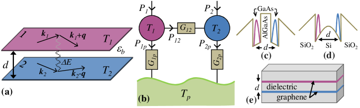
The investigations of bilayer carrier systems have been focused on the drag phenomenon, but the interlayer interaction also mediates energy and heat transfer between the layers (see Fig. 1) and such near-field energy/heat transfer is the topic of the present Paper. Considerable efforts have been devoted to understand near-field heat transfer via different channels between bodies that are separated by a small vacuum
gap.Pendry (1999); Joulain et al. (2005); Volokitin and Persson (2007) One of the most significant heat exchange channels is built from inter-body photon coupling. Surface excitations involving optical phonons and plasmons can play an important role and these so-called polariton effects can strongly enhance the near-field energy transfer.Joulain et al. (2005) Recently, a near-field heat transfer channel arising directly from lattice vibrations has also been proposed.Prunnila and Meltaus (2010); Altfeder et al. (2010) Near-field heat transfer is naturally always present between closely spaced systems, even in the case of solid contact, but then the effect is expected to be strongly masked by competing heat dissipation channels formed by solid heat conduction and/or electron-phonon coupling. One of the motivation for the present work is to challenge this line of thought and, indeed, by detailed calculations we will show that in bilayer carrier systems the near-field heat transfer can become the dominant interlayer heat transfer mechanism.
In this work, we derive general expression of charge fluctuation induced interlayer energy transfer rate, which is applicable to semiconductor and graphene bilayers. In the derivation we use perturbation theory and fluctuation-dissipation relations. Our formula for the interlayer thermal conductance, , has strong connection to the drag resistance formulasFlensberg et al. (1995). The interlayer thermal conductance is intimately connected to fluctuations and dissipative properties of the individual layers. This is explicitly seen as the presence of the imaginary parts of the layer susceptibilities in the formula and it is a manifestation of fluctuation-dissipation theorem. Approximation formulas and detailed calculations of in the case of screened Coulomb interlayer interaction are presented and we show that interlayer thermal transport is strongly enhanced due to disorder. As the layers are in the same solid there exist competing energy relaxation channels. At the temperatures of interest electron-phonon coupling to the bulk thermal phonons is the relevant competing heat dissipation mechanism [see Fig. 1(b)]. It is shown that remarkably can dominate over the electron-phonon coupling. Therefore, near-field heat transfer can become a dominant heat transfer mechanism even in the case of solid contact.
II Theory
In this Section we derive general expression for the interlayer thermal conductance . Then we introduce approximation formulas for and on the basis of the existing literature discuss electron-phonon coupling, which is the competing dissipation channel.
II.1 Interlayer thermal conductance
The scattering events depicted in Fig. 1(a) are mediated by interlayer interaction which is described by matrix element (to be defined later). The interlayer Hamiltonian is given by
| (1a) | |||||
| (1b) | |||||
where is the area, is the electron density operator for layer and is the electron annihilation (creation) operator. Variables and are wavevector, band index and spin index, respectively (here we will assume spin degeneracy). All electron variables depend on the layer index , but this is typically not written explicitly (e.g. ). Factor is defined by the wavefunction of the single particle states and product defines a band form factor. For an ideal 2D electron gas (2DEG) we have and summation over band indices can be ignored. For graphene we have , where and denote conduction and valence bands, respectively, and .
Next, will be considered as a perturbation Hamiltonian that will cause transitions from initial state with energy to final state with energy . Here () is the initial (final) state of layer . The transition rate from initial state to final state is given by the golden rule formula
| (2) |
By multiplying by the energy change and performing an ensemble average over the initial electronic states, and summing over final electronic states we obtain energy transfer rate (heat transfer)
| (3) |
where is the weighting factor of carrier layer in state . We assume that each layer can be described by a local temperature and, therefore, . By using the identity and definition of correlator
| (4) |
we find
| (5) |
As we assume internal equilibrium for the different layers we can adopt the fluctuation-dissipation relation Kubo (1966) Im, where is the susceptibility, which can depend on . Using the fluctuation-dissipation relation and the property we find the general expression for the interlayer heat transfer
| (6) |
where . At the limit it is useful to define the interlayer thermal conductance . From Eq. (6) we find
| (7) |
which has a striking similarity with the bilayer drag resistance formula.Flensberg et al. (1995) Equation (7) has only single temperature and, therefore, it is more convenient to adopt in the case studies instead of Eq. (6).
In the following we will assume that the interlayer interaction is mediated by screened Coulomb interaction, when the matrix element is given by where is the 2D Fourier transform of Coulomb potential ( is the background dielectric constant) and is the spatial form factor, which depends on the spatial extent of the electron wave functions and layer distance . For graphene the extend is practically zero and for the sake of simplicity here we assume vanishing extent for the semiconductor systems as well. Thus, we use . The inter-layer dielectric function is given by .Rojo (1999); Flensberg et al. (1995)
In the ballistic limit the carrier mean free path exceeds the layer distance ( ) and we use the ideal 2D susceptibilities. For 2DEG we have Stern (1967)
| (8) |
where , , , , and for , and and for . Here () is the Fermi velocity (wave vector) and is the density of states at Fermi level . For ballistic graphene the expression for is quite lengthy and will not be presented here. It can be found, for example, from Ref. Hwang and Sarma (2007).
II.2 Approximation formulas
Even though there are some fundamental differences between graphene and 2DEGs, the response of these systems is similar at low frequencies and small . Indeed, for the Taylor series expansion of 2DEG [Eq. (8)] and graphene susceptibilities Hwang and Sarma (2007) we find the same result
| (9) |
Respectively, in the diffusive limit () the susceptibility can be approximated as
| (10) |
where is the diffusion coefficient and is the momentum relaxation time.
By using Eq. (9) in Eq. (7) for two similar ballistic 2DEG and graphene layers we find asymptotic low-temperature result
| (11) |
where , is the screening wave vector and . The above Equation provides a good approximation when . Note that parameter characterizes the screening of the interlayer interaction: large (small) means strong (weak) screening.
In the diffusive limit we use Eq. (10) in Eq. (7) and we find low temperature approximation formula
| (12) |
Here is the DC conductivity of single layer and . Equation (12) is applicable when . Note that the diffusive [Eq. (12)] greatly exceeds the one in the ballistic case [Eq. (11)], which is the manifestation of enhanced fluctuations and dissipation due to disorder.
II.3 Electron-phonon coupling
As depicted in the thermal circuit of Fig. 1(b) competes with the electron-phonon thermal conductance , which at the limit is given by . In 2DEGs at low temperatures the electron-phonon energy transfer is dominated by screened deformation potential () and piezoelectric () interaction with total thermal conductance . For the deformation potential contribution we have Price (1982); Prunnila (2007)
| (13) |
where represents ballistic (diffusive) limit of electron-phonon coupling, for which we have . Here is the thermal phonon wave vector, factor , is the longitudinal (transversal) phonon velocity and is the mass density of the crystal. The brackets stand for solid angle average and is the angle with respect to the z-axis, which is perpendicular to the layer plane. is an effective deformation potential coupling and and . Parameter and as a result . The piezoelectric coupling gives rise to contribution Price (1982); Prunnila (2007); Khveshchenko and Reizer (1997)
| (14) |
where is the effective piezo coupling. For graphene the electron-phonon coupling is dominated by deformation potential coupling Viljas and Heikkilä (2010) and vector potential coupling Chen and Clerk (2012) () giving . For these both contributions we will use directly the results of Ref. Chen and Clerk (2012).
III Results and discussion
In this section, we calculate the interlayer thermal conductance of selected semiconductor and graphene bilayer systems at the ballistic and diffusive limit and discuss possible experimental configurations to investigate . Interlayer thermal conductance will be compared to electron-phonon thermal conductance . Diffusive is considered at larger interlayer separation than the ballistic one in order to assure that the diffusive response formula [Eq. (10)] is valid and condition is fulfilled.
III.1 Calculations for different bilayers
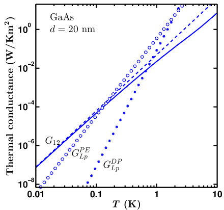
Figure 2 shows obtained numerically from Eqs. (7) and (8) in the case of symmetric high mobility (ballistic) GaAs bilayerGramila et al. (1991) [depicted in Fig. 1(c)] with single layer electron density m-2 and nm. Asymptotic limit formula of Eq. (11) is also plotted. In the phonon contribution we have , where eV is the dilatational deformation potential constant, and , where C/N is the only non-zero element of the piezotensor. Other parameters can be found from Ref. Madelung (2004). Equations (13) and (14) are plotted as symbols in Fig. 2 in the ballistic limit of electron-phonon coupling. Below few Kelvin piezoelectric coupling fully dominates and as a result the temperature regime where is pushed towards relatively low, but experimentally achievable, temperatures. The crossover occurs at mK.
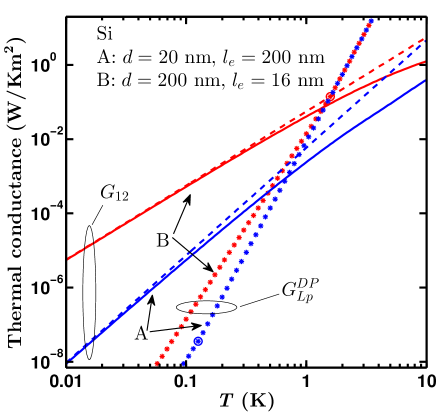
For silicon based bilayer [see Ref. Takashina et al. (2004); *prunnila:2005 and Fig. 1(d)] we consider both ballistic and diffusive limits at electron density m-2. Parameters for Si can be found from Ref. Madelung (2004). The curves in Fig. 3 are calculated for symmetric high (low) mobility Si bilayer system with mobility () mVs, mean-free path () nm and layer distance () nm. For the high mobility device we have used the ballistic limit response [Eq. (8)] and for the low mobility one the diffusive response [Eq. (10)]. Silicon is not piezoelectric so for we need to consider only .Due finite electron mean free path (even for the high mobility device) we will include ballistic and diffusive limits of . For simplicity we plot so that it changes abruptly from diffusive to ballistic formula [note that Eq. (13) is not valid close to ]. For Si 2DEG we have and , where is the uniaxial deformation potential constant. We use the typical values eV. For the high and low mobility Si systems the crossover temperature where is mK and K, respectively. Even though we have set an order of magnitude larger for the diffusive device, still the crossover occurs at higher temperature, which is the signature of the enhancement of fluctuations/dissipation and, thereby, interlayer coupling due to disorder. Note that deformation potential electron-phonon coupling is also enhanced due to disorder.
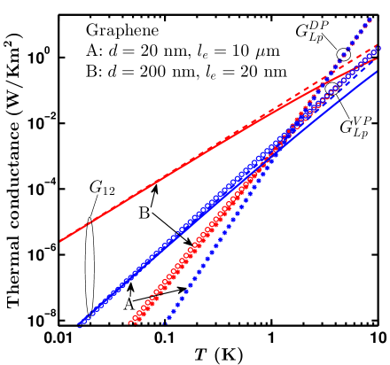
The curves in Fig. 4 are calculated for symmetric high (low) mobility device with mobility () mVs, mean-free path m ( nm), layer distance () nm and electron density m-2. We have used m/s and assumed AlO dielectric between the layers. As above, for the high mobility and for low mobility device we use ballistic and diffusive response functions, respectively. Screened deformation potential and vector potential electron-phonon contributions are plotted in Fig. 4 as symbols. For high mobility graphene dominates at the lowest temperatures and the cross-over where occurs at relatively low temperature of mK. The disorder enhancement of the interlayer heat transfer pushes the threshold for low mobility graphene to K. Note that the vector potential electron-phonon coupling is decreased with the disorder in contrast to deformation potential coupling.
Another widely explored semiconductor bilayer carrier system, which can be realized using compound semiconductorsSivan et al. (1992) or SiPrunnila et al. (2008); Takashina et al. (2009), is the electron-hole bilayer. The complexity of the valence band makes this system more difficult to analyze theoretically. We will not present for such system here explicitly, but it should behave in similar fashion as its electron-electron counter part. However, one thing that may differ drastically from electron-electron bilayer system is the carrier-phonon coupling. Due to asymmetry in the deformation potential coupling between the different layers the carrier-phonon coupling can be unscreened and as a result can be strongly enhanced at low temperatures. Prunnila (2007) The enhancement factor depends on the details of the system, but in many cases it is of the order of , which suggests that for semiconductor electron-hole bilayers can dominate over even down to very low temperatures. Note that also in symmetric electron bilayers can be affected by the presence of another carrier system in non-trivial way, but significant enhancement is not expectedPrunnila (2007).
III.2 Possible experimental realizations
The interlayer heat transfer can be investigated experimentally by varying the input powers while measuring the electron temperatures [see Fig. 1(b)]. Uniform input power follows, for example, from Ohmic heating. This technique has been broadly utilized in the electron-phonon coupling measurements. Indeed, the electron-phonon contributions can be investigated independently from at balanced input power that gives . In the case of semiconductor bilayer the other layer can be also depleted to get a handle on . Note that the Ohmic heating technique has been utilized also in the investigation of coupling of Johnson-Nyquist noise heating between two resistors at different temperatureMeschke et al. (2006), which is conceptually very close to the case presented here.
It is not necessarily trivial to measure electron temperature of the individual layers. For example, quantum corrections of resistivity and Shubnikov- de Haas oscillations, that have been used as electron thermometer, can be affected by the other layer in a complicated way. More local temperature probes based, e.g., on quantum point contacts and quantum dots have also been investigated.Appleyard et al. (1998); Prance et al. (2009); Gasparinetti et al. (2012) Noise thermometry provides an attractive way to probe electron temperature. It has been recently used for single layer graphene Fong and Schwab (2012) and could be adopted in investigations of .
Interlayer heat transfer can also be investigated in more indirect way by coupling the individual layers to metallic electrodes, to which the input power is fed and where temperature is sensed. As metals have quite large electron-phonon coupling the volume of the metallic islands should be sufficiently small in order not to hide . Especially in the case of Si, doped contact regions can serve as the metallic islands. This is attractive approach as the electron-phonon coupling in doped semiconductors can be relative weak so that still dominates. The sign of can be also reversed, which is equivalent to cooling. This can be achieved by quantum dots Prance et al. (2009) or semiconductor-superconductor contacts Savin et al. (2001).
As (and ) depends on the electron densities and on the interlayer density balance it is desirable to adjust the layer densities by external gates. In general, could be used as a gate voltage controlled thermalization path (thermal switch). However, it is important to note (as already pointed out in Ref.Prunnila (2007)) that similar near-field thermal coupling to can exist between the 2D carriers and the external gate electrodes.
IV Summary and conclusions
In summary, a near-field heat transfer effect due to interlayer interaction in bilayer carrier systems was investigated. By using perturbation theory and fluctuation-dissipation relations we derived a general expression of near-field interlayer energy transfer rate [Eq. (6)] and thermal conductance [Eq. (7)]. Our formulation can be applied, for example, to semiconductor and graphene based bilayers. We presented analytical approximation formulas and detailed calculations of interlayer heat transfer due to screened Coulomb interaction for GaAs, Si and graphene based bilayers. It was shown that remarkably the interlayer heat transfer can dominate over the electron-phonon coupling to the thermal bath below a crossover temperature that depends on the system parameters. We found a crossover temperature of mK ( mK) for ballistic GaAs (Si) bilayer with nm layer distance and carrier density m-2 ( m-2). Strong vector potential electron-phonon coupling in ballistic graphene results in low crossover temperature of mK ( m-2). Interlayer heat transfer is enhanced by disorder and for low mobility Si (graphene) bilayer with nm the crossover occurs already at K ( K). The crossover temperatures reported here can be accessed by standard experimental equipment and we introduced possible experimental configurations to investigate the interlayer heat transfer.
Finally, we note that by lowering the electron densities and/or by increasing the temperature plasmons and virtual phonons may start to play a role in the interlayer interaction. These excitations are known to enhance the bilayer drag effect Flensberg and Hu (1994); Bønsager et al. (1998) and the enhancement should also be observable in the interlayer heat transfer. In a very dilute and strongly interacting systems enhancement of drag, that cannot be explained with plasmons or virtual phonons, has also been observed.Pillarisetty et al. (2002) Therefore, depending on the system parameters the crossover temperature, below which the interlayer heat transfer starts to dominate over the electron-phonon coupling to the thermal bath, can be significantly higher than the ones given in this work. Studies of plasmonic effects, virtual phonon excitations, dilute carrier regime and elevated temperatures are left for future investigations. At elevated temperatures the effect described in this paper can also be of relevance for inter-flake heat transfer in thermal interface materials fabricated from graphene composites.Shahil and Balandin (2012) The concepts presented in this work can be extended to coupled one-dimensional carrier systems.
Acknowledgements.
The authors want to acknowledge useful discussions with P.-O. Chapuis, K. Flensberg and D. Gunnarsson. This work has been partially funded by the Academy of Finland through grant 252598 and by EU through project 256959 NANOPOWER.References
- Rojo (1999) A. G. Rojo, J. Phys. Condens. Matter 11, R31 (1999).
- Das Gupta et al. (2011) K. Das Gupta, A. F. Croxall, J. Waldie, C. A. Nicoll, H. E. Beere, I. Farrer, D. A. Ritchie, and M. Pepper, Advances in Condensed Matter Physics 2011, 727958 (2011).
- Gramila et al. (1991) T. J. Gramila, J. P. Eisenstein, A. H. MacDonald, L. N. Pfeiffer, and K. W. West, Phys.Rev.Lett. 66, 1216 (1991).
- Kim et al. (2011) S. Kim, I. Jo, J. Nah, Z. Yao, S. K. Banerjee, and E. Tutuc, Phys. Rev. B 83, 161401 (2011).
- Pendry (1999) J. B. Pendry, J. Phys.: Condens. Matter 11, 6621 (1999).
- Joulain et al. (2005) K. Joulain, J.-P. Mulet, F. Marquier, R. Carminati, and J.-J. Greffet, Surface Science Reports 57, 59 (2005).
- Volokitin and Persson (2007) A. I. Volokitin and B. N. J. Persson, Rev. Mod. Phys. 79, 1291 (2007).
- Prunnila and Meltaus (2010) M. Prunnila and J. Meltaus, Phys. Rev. Lett. 105, 125501 (2010).
- Altfeder et al. (2010) I. Altfeder, A. A. Voevodin, and A. K. Roy, Phys. Rev. Lett. 105, 166101 (2010).
- Flensberg et al. (1995) K. Flensberg, B. Hu, A. Jauho, and J. M. Kinaret, Phys. Rev. B 52, 14761 (1995).
- Kubo (1966) R. Kubo, Rep. Prog. Phys. 29, 255 (1966).
- Stern (1967) F. Stern, Phys. Rev. Lett. 18, 546 (1967).
- Hwang and Sarma (2007) E. H. Hwang and S. D. Sarma, Phys. Rev. B 75, 205418 (2007).
- Price (1982) P. J. Price, J. Appl. Phys. 53, 6863 (1982).
- Prunnila (2007) M. Prunnila, Phys. Rev. B 75, 165322 (2007).
- Khveshchenko and Reizer (1997) D. V. Khveshchenko and M. Y. Reizer, Phys. Rev. Lett. 78, 3531 (1997).
- Viljas and Heikkilä (2010) J. K. Viljas and T. T. Heikkilä, Phys. Rev. B 81, 245404 (2010).
- Chen and Clerk (2012) W. Chen and A. A. Clerk (2012), eprint arXiv:1207.2730.
- Madelung (2004) O. Madelung, Semiconductors: Data Handbook (Springer, 2004).
- Takashina et al. (2004) K. Takashina, Y. Hirayama, A. Fujiwara, S. Horiguchi, and Y. Takahashi, Physica E 22, 72 (2004).
- Prunnila et al. (2005) M. Prunnila, J. Ahopelto, and H. Sakaki, Phys. Stat. Sol.(a) 202, 970 (2005).
- Sivan et al. (1992) U. Sivan, P. M. Solomon, and H. Shtrikman, Phys.Rev.Lett. 68, 1196 (1992).
- Prunnila et al. (2008) M. Prunnila, S. J. Laakso, J. M. Kivioja, and J. Ahopelto, Appl. Phys. Lett. 93, 112113 (2008).
- Takashina et al. (2009) K. Takashina, K. Nishiguchi, Y. Ono, A. Fujiwara, T. Fujisawa, Y. Hirayama, and K. Muraki, Appl. Phys. Lett. 94, 142104 (2009).
- Meschke et al. (2006) M. Meschke, W. Guichard, and J. P. Pekola, Nature 44, 187 (2006).
- Appleyard et al. (1998) N. J. Appleyard, J. T. Nicholls, M. Y. Simmons, W. R. Tribe, and M. Pepper, Phys. Rev. Lett. 81, 3491 (1998).
- Prance et al. (2009) J. R. Prance, C. G. Smith, J. P. Griffiths, S. J. Chorley, D. Anderson, G. A. C. Jones, I. Farrer, and D. A. Ritchie, Phys. Rev. Lett. 102, 146602 (2009).
- Gasparinetti et al. (2012) S. Gasparinetti, M. J. Martinez-Perez, S. de Franceschi, J. P. Pekola, and F. Giazotto, Applied Physics Letters 100, 253502 (2012).
- Fong and Schwab (2012) K. Fong and K. Schwab (2012), eprint arXiv:1202.5737.
- Savin et al. (2001) A. M. Savin, M. Prunnila, P. P. Kivinen, J. P. Pekola, J. Ahopelto, and A. J. Manninen, Appl. Phys. Lett. 79, 1471 (2001).
- Flensberg and Hu (1994) K. Flensberg and B. Y.-K. Hu, Phys. Rev. Lett. 73, 3572 (1994).
- Bønsager et al. (1998) M. C. Bønsager, K. Flensberg, B. Yu-Kuang Hu, and A. H. MacDonald, Phys. Rev. B 57, 7085 (1998).
- Pillarisetty et al. (2002) R. Pillarisetty, H. Noh, D. C. Tsui, E. P. De Poortere, E. Tutuc, and M. Shayegan, Phys. Rev. Lett. 89, 016805 (2002).
- Shahil and Balandin (2012) K. M. Shahil and A. A. Balandin, Solid State Communications 152, 1331 (2012).