High-Q Gold and Silicon Nitride Bilayer Nanostrings
Abstract
Low-mass, high-, silicon nitride nanostrings are at the cutting edge of nanomechanical devices for sensing applications. Here we show that the addition of a chemically functionalizable gold overlayer does not adversely affect the of the fundamental out-of-plane mode. Instead the device retains its mechanical responsiveness while gaining sensitivity to molecular bonding. Furthermore, differences in thermal expansion within the bilayer give rise to internal stresses that can be electrically controlled. In particular, an alternating current (AC) excites resonant motion of the nanostring. This AC thermoelastic actuation is simple, robust, and provides an integrated approach to sensor actuation.
Silicon nitride nanostrings Ver06 ; Ver08a are an exciting class of mechanical resonator, exceptional for their ultra-high quality factors (s),Sch11a their tolerance to irregularities in the fabrication process (since their resonant frequencies depend only on the device length),Ver08b their harmonic normal mode spectrum, and the ease with which their vibrational motion can be detected optically (by virtue of the low absorption of silicon nitride at visible wavelengths).Unt09 ; Unt11 ; Dav10a ; Suh12 ; Ane09 ; Fon10 But in order for these devices to be used efficiently in room temperature molecular sensing applications,Ber97 ; Arl11 they should have a surface that is chemically functionalizable. Silicon nitride, however, is largely inert.
The most common workaround, routinely carried out with silicon and silicon nitride atomic force microscope (AFM) cantilevers, is to coat the resonator with gold. Then a molecule of choiceGru11 can be affixed to the gold overlayer, attached by way of a thiol intermediary.Mar02 ; God04 The addition of the gold has no adverse consequences for static, stress-response measurements,God10 but it generally does for measurements that are dynamic in nature. For example in the cantilever case, metallization causes significant dissipation in the resonator, San05 lowering its and reducing its usefulness as a sensor—although this can be circumvented by depositing only in areas that do not become stressed upon actuation.Sos11 ; Lab12
Accordingly, our initial expectation was that application of a uniform gold layer to a silicon nitride nanostring would ruin the device’s ultra-high , which is typically on the order of but can be as high as (see Ref. Sch11a, ). Instead, we show here that a 53 nm thick metallic layer on top of a 250 nm thick silicon nitride nanostring does not adversely affect the of the fundamental frequency, even though it nearly doubles the total mass of the string. (Our longest gold-covered device, at 210 m, has for the fundamental mode and a total mass of pg.) It does, however, reduce the s associated with higher harmonics, so that the –versus–resonant-frequency behavior that was previously flat (up to even-odd effects across modes) now decays with frequency. This change is characteristic of a string system whose dominant dissipation mechanism is no longer localized at the anchor points.Suh12
Another important feature of the gold layer is that it renders the string sensitive to temperature through the bimaterial effect (a differential stress between the gold and silicon nitride layers due to different coefficients of thermal expansion).Gim94 ; Bar94 ; Var97 While this could prove useful in temperature sensingLar11 or provide an independent measurement of the resonator temperature,Cha12 our focus lies elsewhere. In particular, we demonstrate that it is possible not only to vary the temperature of the device electrically via direct current (DC) ohmic heating but to actuate resonant motion via alternating current (AC) thermoelastic heating. Both the DC and AC effects have practical uses for sensors: the first allows for device regeneration (i.e., it provides a mechanism to desorb molecules, returning the device to a clean state), which facilitates thermal studies of affixed molecules Ber98 ; Zha11 ; Yi08 ; Ier11 ; Liu12 and, as recently shown,Cha12 can provide exceptional frequency stability in ultra-low-noise nanomechanical sensing; the second provides integrated actuationBar07 ; Seo08 ; Vil11 and obviates the need for a piezoelectric buzzer or other external driving mechanism.
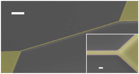
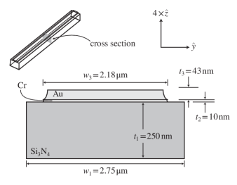
Fabrication of the bilayer nanostrings is straightforward, since only one lithography step is necessary. We start with stoichiometric silicon nitride (250 nm) deposited onto silicon dioxide (2 m) on a silicon handle (Rogue Valley Microdevices). This is subsequently sputtered with 10 nm of chromium, followed by 43 nm of gold. (We refer to the resulting device as bilayer nanostring, since the intermediate chromium layer is thin and serves only an adhesion function.) Standard optical lithography is then performed. This is followed by wet etching of the gold and then chromium, reactive ion etching of the silicon nitride, and device release with a buffered oxide etch of the silicon dioxide. The resulting strings are shown in Fig. 1. The gold is slightly over-etched, although this is not important since the string’s normal modes are insensitive to the exact dimensions. This fault tolerance during fabrication is advantageous for bulk processing.
Measurements are performed by optical interferometry using a 632.8 nm laser focused onto the nanostring, as described elsewhere, Dav10b ; Suh12 inside an optical access vacuum chamber in which the temperature of the sample stage can be controlled and accurately determined. The optical power incident on the device is W—below the onset of optical heating effects. The interferometric signal is amplified 25-fold after detection and is analyzed using a high frequency lock-in amplifier (Zurich Instruments HF2LI), which allows us to extract the peak frequency and by fitting to the power spectral density function (PSD) (see supplementary material of Ref. Suh12, ). This analysis is appropriate regardless of the actuation method: thermomechanical, external piezoelectric, or integrated ohmic (thermoelastic). In addition, our optical system can be scanned with respect to the sample using closed-loop piezo stages,Dav10b providing spatial maps of the amplitude and phase output by the Zurich lock-in. Hence, we can unambiguously distinguish between in-plane and out-of-plane motion.
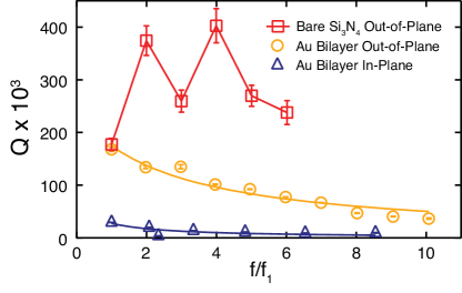
We emphasize that while we have verified the following results using numerous nanostrings of varying lengths, for consistency we present data for a single 210 m long by 2.75 m wide bilayer nanostring with an initial resistance of 176 . The s of this bilayer nanostring in vacuum ( torr) are shown in Fig. 2. These s are compared with out-of-plane modes of uncoated strings of a very similar geometry (red squares) from Ref. Suh12, . It is immediately clear that the of the fundamental out-of-plane mode is essentially unchanged (although the resonant frequency itself is reduced by about 25% because of the addition of the gold). This device is therefore an excellent candidate for a functionalizable, high- nanomechanical sensor.
On the other hand, the higher order modes are damped as compared to the bare string. Both bare and gold bilayer devices demonstrate the alternating even/odd behavior previously seen for silicon nitride membranesWil11 and nanostrings,Suh12 which has been reported to originate from dissipation due to phonon tunneling.Wil11 Ignoring this oscillation, the of the bare device is essentially flat with respect to frequency (or, equivalently, mode number). The of the gold bilayer strings, however, decays with frequency. A key difference appears to be the high thermal conductivity of the metallic layer, which allows for efficient transport of energy from within the string (dissipated as a result of internal stresses during bulk bending) to the outside.
As we have previously shown,Suh12 the varies by mode according to
| (1) |
The tilde decorated quantities are damping coefficients from which the leading order frequency dependence has been factored out. The viscous damping term, , can be neglected since the experimental chamber has been evacuated far past the point where the measured exhibits a pressure dependence.Ver08b In the case of the bare string, is the overwhelmingly dominant contribution; Suh12 energy is lost primarily in dissipative processes in the vicinity of the anchor points, and the has no frequency dependence other than the even/odd mode effect. The of the gold bilayer string, however, shows a decaying tail that can only be fit with a non-vanishing term, attributable to bulk dissipation. Specifically, we find from the out-of-plane data in Fig. 2 that . Determination of the microscopic bulk dissipation mechanism would require further detailed studies.Moh02 We remark that the s of the higher order modes are still rather impressive (), suggesting that this device can be used for multimode sensing. Doh07 ; Sch10
Beyond altering the dissipation, the gold overlayer adds functionality to the nanostring system by introducing bimaterial temperature dependence. In particular, we have observed that the resonant frequencies of the nanostring shift with heating. There are two scenarios to consider: (i) the sample stage is held in thermal equilibrium at a uniform temperature ; (ii) heating is highly localized in the string, and the rest of the system—including the supports and substrate—can be viewed as a heat bath at . The second scenario corresponds to the Joule heating case in which a current is passed through the metallic overlayer.
In the first scenario, the frequencies have the form
| (2) |
where are the relative thermal expansion coefficients measured with respect to that of the substrate, , and the parameters , are the corresponding Young’s moduli and cross-sectional areas. (See Ref. Lar11, and references therein.) These material parameters are defined for each layer with the indices (silicon nitride), (chromium), and (gold).
For small temperature changes, it is sufficient to consider the linearized relative frequency shift
| (3) |
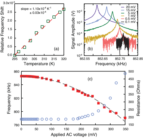
We observe that the prefactor to is either positive or negative depending on the value of . For our device, the frequency of the resonator shifts upward with heating since the thermal expansion coefficient of the substrate, , is larger than , an effective alpha of the string that depends on the expansion coefficients of the constituent materials, averaged layer-wise according to the product of the cross-sectional area and Young’s modulus. Hence, the string is stretched tighter as the temperatures goes up; the relative expansion of the string increases the effective tensile stress, and the resonances shift to higher frequencies. Putting reasonable estimates of the material parametersSM into Eq. (3), we predict for the slope in Fig. 3(a). This is consistent with the observed value, .
In the second scenario, resistance to an electrical current through the metallic layer of the string causes local heating. The substrate is unaltered and only the string deforms. The frequency shift then has the same form as Eq. (2) but with each replaced by its bare value and, if the current is alternating, with understood to be the time-averaged temperature variation.
We can model the resistive heating in a simple way. If a constant power is applied to the string, the total excess heat energy comes into equilibrium when Here, represents the half-life for thermal energy to leak out of the string. The energy outflow can be computed as a sum of thermal currents (of the form ) driven by a gradient . We make use of the device’s overall heat capacity to relate the change in heat energy to a corresponding change in temperature and thus to produce an estimate of
| (4) |
(Values of the density , specific heat , and thermal conductivity are tabulated per layer in the supplementary material.SM ) Note that scales as , since the equilibration process is essentially diffusive; this implies that, near resonance, . Because the layers themselves come into local thermal equilibrium on a fast time scale of around (where and are the thickness and width of the silicon nitride respectively), we proceed as if the silicon nitride, chromium, and gold layers are at the same temperature instantaneously at each point along the string. This is a safe assumption up to a frequency scale , which is well above the oscillation frequency of any of the harmonic modes that we can measure in our device.
The simple analysis we have outlined is primarily limited by the fact that we have supposed the temperature profile to have no meaningful variation along the length of the string. Still, it reliably captures the fact that the thermal time scale is on the order of microseconds (rather than nanoseconds, as for the device described in Ref. Bar07, ), orders of magnitude faster than the time for the mechanical energy to be transferred to the environment, as dictated by the high of the string: ms.
In our AC local heating scenario, the power pumped into the string is given by , where is the string’s electrical resistance and is the alternating voltage applied across the string. Since the silicon nitride is insulating (), we can estimate the resistance from the geometry of the device using standard values , for the resistivity of Cr and Au: . The 176 we measure experimentally is higher, mainly because it includes the resistance of the metallic supports. Accordingly, the heat content of the string (ignoring the initial transient) varies in time as
| (5) |
with a phase lag that depends only on the thermal outflow time . We can decompose the corresponding temperature variation into a time-invariant background over which is superposed the weaker, alternating behaviour . Hence, the analogue of Eq. (3) is
| (6) |
The relative frequency shift is quadratic in and always negative—consistent with our observations in Fig. 3(c). In contrast to the relative frequency shift described by Eq. (3), which is insensitive to the device length, the effect described in Eq. (6) is predicted to scale as (and thus can be made arbitrary large by choosing a long enough string). The predicted coefficient, 6.82 V-2, is about ten times larger than the value obtained from a fit to the data. Theory and experiment can be made to coincide if instead we take the thermal time to be s. The discrepancy likely stems from the over-simplified, uniform temperature profile along the length of the string.
In the vicinity of the fundamental mode of our device, , so that has essentially achieved its maximum value, . In this limit, , and the magnitude of the alternating component of the temperature with respect to the average goes as . What’s astonishing is that this tiny alternating local heating is sufficient to actuate the device and to do so very efficiently. Specifically, we are able to use this local heating to actuate the bilayer nanostring by passing an AC current along the length of the device. Note that this is subtly different from the bimaterial effect in cantilevers and non-uniformly coated beams, where the gold exerts a force on the cantilever that pushes it towards the substrate.Bar07 ; Seo08 ; Vil11 In such a scenario, the force is directional, and hence the AC drive voltage must be applied at frequency in order to produce heating and bending at . In contrast, in our system there is no preference towards or away from the substrate as the gold expands, since it forms a continuous layer over the string. Heating and bending occur twice per string oscillation, and therefore the applied drive voltage and resulting motion have the same frequency. We are also able to actuate the device at , although times less efficiently—consistent with the above scenario.
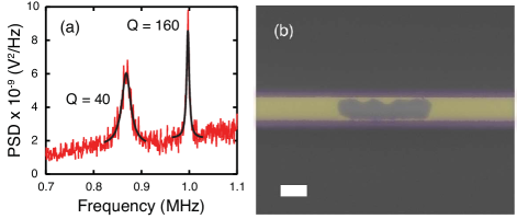
In Fig. 3(b), we show frequency sweeps using the reference output of the Zurich lock-in amplifier to resonantly drive the nanostring. This integrated electronic actuation scheme is simple, compact, and robust. With root-mean-square AC voltages as small as V we can clearly detect resonant motion, while the maximum signal-to-noise is achieved with approximately to mV. At higher drives the nanostring becomes nonlinear. Yet even at quite high drives, in vacuum, we see no change in the resistance of the gold layer. Hence the local heating of the bilayer nanostring is nondestructive to the gold layer in the linear actuation regime and beyond. In addition, we note that the resonance frequency is entirely non-hysteretic at these actuation voltages—further evidence that the AC ohmic actuation scheme is robust. Only at voltages mV, approximately 10 times that required for optimal signal-to-noise, is there an onset of resistance changes in the gold layer. The device continues to function with applied voltages in excess of mV, after which it rapidly becomes an open circuit. Using the extracted value s, we can estimate that the upturn in resistance, appearing at mV in Fig. 3(c), begins when the device has been heated an additional K and that burn out occurs when mV and K. SEM of our device, shown in Fig. 4(b), reveals that the gold has only been removed from a small patch on the string surface yet has interrupted the current path.
Finally we note that the AC ohmic actuation technique works for both higher-order harmonics in vacuum (not shown) as well as for the fundamental modes in air. In the ambient pressure case, the nanostrings experience strong viscous damping, especially when the motion is perpendicular to the string’s substantial width. The of the first out-of-plane mode is only 40 while that of the in-plane mode is 160 [see Fig. 4(a)]. There is a greater cross-section for molecular collisions, and thus energy loss, in the out-of-plane direction. The voltages required to actuate the nanostring in air ( mV) result in resistance changes and eventual failure. Improving the in viscous environments Li07 ; Sun11 would decrease the required actuation voltages and prevent such failure.
In conclusion, gold bilayer nanostrings are an enhancement to the already exciting system of silicon nitride nanostrings. They enable chemical functionalization and molecular detection, provide a scheme for local heating to study thermal response of molecules or desorb unwanted molecules, and provide simple and integrated actuation. And unlike traditional micromechanical resonators,San05 they maintain their high quality factors even with a continuous metallic coating.
This work was supported by the University of Alberta, Faculty of Science; the Canada Foundation for Innovation; the Natural Sciences and Engineering Research Council, Canada; and the Canada School of Energy and Environment. We thank J.M. Gibbs-Davis and M.R. Freeman for helpful discussions, and thank Don Mullin, Greg Popowich and the University of Alberta NanoFab staff for technical assistance.
References
- (1) S.S. Verbridge, J.M. Parpia, R.B. Reichenbach, L.M. Bellan and H.G. Craighead, J. Appl. Phys. 99, 124304 (2006).
- (2) S.S. Verbridge, H.G. Craighead and J.M. Parpia, Appl. Phys. Lett. 92, 013112 (2008).
- (3) S. Schmid, K.D. Jensen, K.H. Nielsen and A. Boisen, Phys. Rev. B 84, 165307 (2011).
- (4) S.S. Verbridge, R. Ilic, H.G. Craighead and J.M. Parpia, Appl. Phys. Lett 93, 013101 (2008).
- (5) Q.P. Unterreithmeier, T. Faust and J.P. Kotthaus, Phys. Rev. Lett. 105, 027205 (2011).
- (6) Q.P. Unterreithmeier, E.M. Weig and J.P. Kotthaus, Nature 458, 1001 (2009).
- (7) J.P. Davis, D. Vick, J.A.J. Burgess, D.C. Fortin, P. Li, V. Sauer, W.K. Hiebert and M.R. Freeman, New Journal of Physics 12, 093033 (2010).
- (8) A. Suhel, B.D. Hauer, T.S. Biswas, K.S.D. Beach and J.P. Davis, Appl. Phys. Lett. 100, 173111 (2012).
- (9) G. Anetsberger, O. Arcizet, Q.P. Unterreithmeier, R. Rivière, A. Schliesser, E.M. Weig, J.P. Kotthaus and T.J. Kippenberg, Nature Phys. 5, 909 (2009).
- (10) K.Y. Fong, W.H.P. Pernice, M. Li and H. X. Tang, Appl. Phys. Lett 97, 073112 (2010).
- (11) R. Berger, E. Delamarche, H. Peter Lang, C. Gerber, J.K. Gimzewski, E.Meyer and H.-J. Güntherodt, Science 276, 2021 (1997).
- (12) J.L. Arlett, E.B. Myers and M.L. Roukes, Nature Nano. 6, 203 (2011).
- (13) K. Gruber, T. Horlacher, R. Castelli, A. Mader, P.H. Seeberger and B.A. Hermann, ACS Nano 5, 3670 (2011).
- (14) R. Marie, H. Jensenius, J. Thaysen, C.B. Christensen and A. Boisen, Ultramicroscopy 91, 29 (2002).
- (15) M. Godin, P. J. Williams, V. Tabard-Cossa, O. Laroche, L.Y. Beaulieu, R.B. Lennox and P.H. Grütter, Langmuir 20, 7090 (2004).
- (16) M. Godin, V. Tabard-Cossa, Y. Miyahara, T. Monga, P.J. Williams, L.Y. Beaulieu, R.B. Lennox and P.H. Grütter, Nanotechnology 21, 075501 (2010).
- (17) R. Sandberg, K. Molhave, A. Boisen and W. Svendsen, J. Micromech. Microeng. 15, 2249 (2005).
- (18) G. Sosale, K. Da, L. Fréchette and S. Vengallatore, J. Micromech. Microeng. 21, 105010 (2011).
- (19) A. Labuda, J.R. Bates and P.H. Grütter, Nanotechnology 23, 025503 (2012).
- (20) J.K. Gimzewski, Ch. Gerber, E. Meyer and R.R. Schlittler, Chemical Physics Letters 217, 589 (1994).
- (21) J.R. Barnes, R.J. Stephenson, C.N. Woodburn, S.J. O’Shea, M.E. Welland, T. Rayment, J.K. Gimzewski and Ch. Gerber, Rev. Sci. Instrum. 65, 3793 (1994).
- (22) J. Varesi, J. Lai, T. Perazzo, Z. Shi and A. Majumdara, Appl. Phys. Lett 71, 306 (1997).
- (23) T. Larsen, S. Schmid, L. Grönberg, A.O. Niskanen, J. Hassel, S. Dohn and A. Boisen, Appl. Phys. Lett 98, 121901 (2011).
- (24) J. Chaste, A. Eichler, J. Moser, G. Ceballos, R. Rurali and A. Bachtold, Nature Nano. 7, 301 (2012).
- (25) R. Berger, H.P. Lang, Ch. Gerber, J.K. Gimzewski, J.H. Fabian, L. Scandella, E. Meyer and H.-J. Güntherodt, Chemical Physics Letters 294, 363 (1998).
- (26) J. Zhao, X. Yin, J. Shi, X. Zhao and J.S. Gutmann, J. Phys. Chem. C 115, 22347 (2011).
- (27) E. Iervolino, A.W. van Herwaarden, W. van der Vlist and P.M. Sarro, J. Microelectromechanical Systems 20, 1277 (2011).
- (28) T. Liu, S. Pihan, M. Roth, M. Retsch, U. Jonas, J.S. Gutmann, K. Koynov, H.-J. Butt and R. Berger, Macromolecules 45, 862 (2012).
- (29) D. Yi, A. Greve, J.H. Hales, L.R. Senesac, Z.J. Davis, D.M. Nicholson, A. Boisen and T. Thundat, Appl. Phys. Lett. 93, 154102 (2008).
- (30) I. Bargatin, I. Kozinsky and M.L. Roukes, Appl. Phys. Lett. 90, 093116 (2007).
- (31) J. H. Seo and O. Brand, J. Microelectromech. Syst. 17, 483 (2008).
- (32) L.G. Villanueva, R.B. Karabalin, M.H. Matheny, E. Kenig, M.C. Cross and M.L. Roukes, Nano. Lett. 11, 5054 (2011).
- (33) J.P. Davis, D. Vick, D.C. Fortin, J.A.J. Burgess, W.K. Hiebert and M.R. Freeman, Appl. Phys. Lett. 96, 072513 (2010).
- (34) I. Wilson-Rae, R.A. Barton, S.S. Verbridge, D.R. Southworth, B. Ilic, H.G. Craighead and J.M. Parpia, Phys. Rev. Lett. 106, 047205 (2011).
- (35) P. Mohanty, D.A. Harrington, K.L. Ekinci, Y.T. Yang, M.J. Murphy and M.L. Roukes, Phys. Rev. B 66, 085416 (2002).
- (36) S. Dohn, W. Svendsen, A. Boisen, and O. Hansen, Rev. Sci. Instrum. 78, 103303 (2007).
- (37) S. Schmid, S. Dohn and A. Boisen, Sensors 10, 8092 (2010).
- (38) See supplementary material at [URL will be inserted by AIP] for details of the device’s geometry and material composition.
- (39) M. Li, H.X. Tang and M.L. Roukes, Nature Nano. 2, 114 (2007).
- (40) X. Sun, K.Y. Fong, C. Xiong, W.H.P. Pernice and H.X. Tang, Optics Express 19, 22316 (2011).
- (41) A. Khan, J. Philip and P. Hess, J. Appl. Phys. 95, 1667 (2004).
- (42) Y. Okada and Y. Tokumaru, J. Appl. Phys. 56, 314 (1984).
- (43) T. Larsen, S. Schmid, L. Grönberg, A.O. Niskanen, J. Hassel, S. Dohn and A. Boisen, Appl. Phys. Lett 98, 121901 (2011).
Supplementary Material
Device geometry
The device is shown in cross section in Fig. S-1. Each of the silicon nitride (), chromium (), and gold () layers is of constant thickness and has an area and a bending moment given by
| (S.1) |
The limits of integration are the cumulative layer thicknesses . The bending axis of the composite string is fixed at a height (measured from the bottom surface) that minimizes the total bending constant . Hence, the values themselves depend indirectly on the Young’s modulus and Poisson ratio of the material in each layer.
Based on our best understanding of the wet- and dry-etch steps in the fabrication process, we propose that the layered string has a width profile of the form
| (S.2) |
The values m and m are estimated from a (top-down) scanning electron microscopy image of the device. We use a pixel-contrast histogram analysis to perform edge detection. Finally, the areas and bending moments have the following values:
| (S.3) |
The device geometry and dimensions we have indicated correspond to a device of total mass 841 pg and heat capacity J/K.
Normal Modes
The layered beam is described by a Lagrangian
| (S.4) |
where is the (uniform) mass per unit length and
| (S.5) |
is the elastic energy density (including tension, elongation, and bending terms) associated with its transverse deformation. penalizes any deviation from the equilibrium position . At this stage, we ignore thermal expansion effects and restrict ourselves to a model that satisfies and . In other words, we assume that the system is invariant under the transformations and , even though the latter symmetry can in principle be broken by the layered structure.
We follow the usual prescription
| (S.6) |
and make use of the variational identities
| (S.7) |
to obtain the equation of motion
| (S.8) |
Here, is the tension in the composite string, and and are its stretching and bending constants. It is sufficient to treat , the term that is nonlinear in , at the mean field level. We do so by replacing by its spatially averaged value
| (S.9) |
Equation (S.8) differs from a pure wave equation by terms that are proportional to the Young’s moduli. The relevant situation here is when these are sufficiently small that the behavior of the system is almost perfectly string-like. When the system is driven in the th pure string mode , it oscillates at an angular frequency
| (S.10) |
For weak nonlinearity, the mean square displacement is small compared to . In that limit,
| (S.11) |
Accordingly, high order modes exhibit a small correction away from a perfectly harmonic spectrum:
| (S.12) |
| thermal | specific | thermal | |||||
| layer (#) | density | Young’s modulus | Poisson ratio | expansion | heat | resistivity | conductivity |
| (g/cm3) | (GPa) | ( K-1) | (J/kgK) | (nm) | (W/mK) | ||
| Au (3) | 79 | ||||||
| Cr (2) | 279 | ||||||
| Si3N4 (1) | 111determined by multimode calibration measurements | 265 | 222from Ref. Khan04, | ||||
| Si (0) | 333from Ref. Oka84, |
Thermal Expansion
Expansion of the layers due to heating leads to a correction that enters the elongation term of the elastic energy density:
| (S.13) |
Note that we are not attempting to model interfacial shearing and peeling stresses. We just assume that the layers are held together by a sufficiently large through-thickness spring constant. Expanding Eq. (S.13) to give
| (S.14) |
we see that the effect of heating is simply to shift the tension. Applying this observation to Eq. (S.11) gives
| (S.15) |
The last line above is correct to the extent that .
Material properties
The properties of silicon nitride thin films are quite different from those of the bulk material. For example, the density and coefficient of thermal expansion are generally lower. So we have taken care to find values that are appropriate to our particular devices.
For the purposes of calibration, we prepare a bare silicon nitride nanostring with no metallic coating. The dimensions of this device are 215 m (length), 2.1 m (width), and 250 nm (thickness). The frequencies (in MHz) of the first six resonant modes are determined to be 1.19508, 2.38389, 3.58222, 4.77447, 5.98263, and 7.19362. In this case, Eq. (S.11) reduces to
| (S.16) |
A best fit of this form to the data produces
| (S.17) |
and hence . We have no direct measurement that closes this set of relations, but if we assume the manufacturer’s quoted value of 0.8 GPa for the tensile stress, then GPa and g/cm3. These values are consistent with other measurements in the literature.Khan04
Furthermore, we obtain the relative frequency shift for each of modes 1, 3, and 5. The measurement is performed over a dense grid of temperature values from 293 K to 320 K and produces a linear slope
| (S.18) |
that is consistent across all three modes. Taking K-1 as the coefficient of thermal expansion for the silicon substrate,Oka84 we find K-1. This is very close to the value K-1 reported in Ref. Lar11, .