Stacking order, interaction and weak surface magnetism in layered graphene sheets
Abstract
Recent transport experiments have demonstrated that the rhombohedral stacking trilayer graphene is an insulator with an intrinsic gap of 6meV and the Bernal stacking trilayer one is a metal. We propose a Hubbard model with a moderate for layered graphene sheets, and show that the model well explains the experiments of the stacking dependent energy gap. The on-site Coulomb repulsion drives the metallic phase of the non-interacting system to a weak surface antiferromagnetic insulator for the rhombohedral stacking layers, but does not alter the metallic phase for the Bernal stacking layers.
In the past several years, the rapid development in preparing few layer graphene samples has promoted great theoretical fzhang ; henrard06 ; min08 ; rmp ; peeters ; koshino ; mccann ; dft ; guo1 ; guo2 ; chou ; dora and experimental tarucha ; lzhang ; kumar ; herrero ; heinz11 ; heinz12 ; jhang ; wbao ; mak interests in such novel quasi-two-dimensional electron systems. The few layer graphene may be a platform for many new physics issues and is of potential application in electronics. One peculiar feature of the layered graphene system is the stacking order, which offers a new route to manipulate the electronic properties in graphene layers.
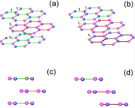
The Bernal (or ABA) stacking and the rhombohedral (or ABC) stacking are two stable stacking orders observed in experiments. As shown in Fig. 1, in either ABA or ABC stacking order, the second graphene sheet is shifted by one bond length along the C-C bond direction. The third graphene sheet is shifted back and aligned with the first sheet in the ABA stacking, while is shifted further by one more bond length along the same direction in the rhombohedral stacking. So the ABA stacking order is ABABAB, and the rhombohedral stacking is ABCABC. The trilayer graphene system is the minimal structure relevant to the stacking orders.
The electronic structures of the graphene layers strongly depend on their stacking orders rmp ; henrard06 ; min08 . In the ABA stacking -layer system, there are electron-like and hole-like parabolic sub-bands touching at for even , and an additional sub-band with a linear dispersion for odd . The states in all the sub-bands are bulk states extended to all the layers. In the ABC stacking layers, the low energy electronic structure is described by two sub-bands with dispersion near the points and in the 2D Brillouin zone. These low energy states are localized on the outermost layers, and are zero modes on the surfaces protected by the topology flat ; sc . In two dimension, the dispersion of gives a density of states , which is divergent for at . This indicates a strong instability toward symmetry broken statesfzhang ; sc .
Trilayer graphene systems are of particular interest for it represents the simplest case for the stacking dependent graphene. Very recently, a stacking dependent intrinsic gap in trilayer graphene has been observed in the transport measurement wbao ; jhang . In the charge neutral case, namely undoped trilayer samples, the experiments indicate that the ABA stacking trilayer graphene is metallic, whereas the ABC stacking trilayer graphene is insulating with an intrinsic gap about 6 meV. Since the non-interacting electronic structure of both stacking orders are gapless hence metallic, the experimental observation of the gap in ABC stacking trilayer is in sharp contraction with the non-interaction picture and points to the importance of the interaction in these systems.
In this Letter, we propose that the observed stacking-dependent metallic or insulting states can be explained by a Hubbard model with a moderate on-site Coulomb repulsion . We use a self-consistent mean field theory to show that the ground state of the ABC stacking trilayer is a weak anti-ferromagnet with opposite ferrimagnetic orderings on the top and bottom layers, due to the divergent density of states in the metallic phase. The magnetic ordering opens a gap, which is in good comparison with the experimental data. Our theory shows that the metallic phase of the ABA stacking trilayer is stable against a moderate Hubbard due to the non-divergent density of state. Our theory is extended to study stacking-dependent graphene systems for larger numbers of layers. We have found that it is a general property for the ABC stacking graphene layers that the on-site Hubbard opens a gap at the Fermi level and leads to a weak surface antiferromagnetic state. Our results can be further tested in future experiments.
We model layer graphene systems by using a Hubbard model , where is a tight binding Hamiltonian to describe the kinetic term of the system and describes the on-site Coulomb repulsion. The chemical potential is set to zero, and the average electron per site is one. The intralayer hopping term is the tight-binding Hamiltonian of independent graphene sheets. For simplicity, we only include nearest neighbor hoppings footnote
| (1) |
where and are the annihilation operators of an electron on sublattices and , respectively. denotes the layer index running from 1 to , and nearest neighbor pairs, and the spin. describes the interlayer hopping given by
| (2) |
for the rhombohedral or Bernal stacking orders. Here, is summed over the two adjacent layers, and is summed over two sites aligned in adjacent layers as shown in Fig. 1. The Hubbard term will be approximated by a mean field Hamiltonian,
| (3) |
where . is determined self-consistently. We consider a spin density wave state and introduce two mean fields on each layer , one for sublattice and one for sublattice , . The mean fields for spin down are related to the spin-up ones, . Note that we have examined possible charge density wave states within the model and found no evidence for that.
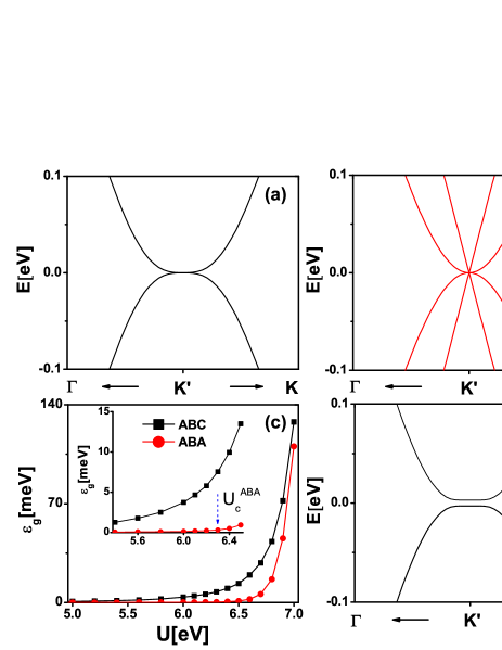
We first examine the trilayer graphenes (). The energy bands for the non-interacting models are shown in Fig. 2 (a) for ABC stacking and in Fig. (b) for ABA stacking with parameters eV and eV. The dispersion in (a) is at small for both conduction and valence bands, which gives rise to a divergent density of states at , and the wave functions for near the or points are localized on the outer surfaces. The energy bands in (b) consist of a parabolic and a linear dispersions, both of which are not localized on the outer surfaces, and the density of states is a constant at . In the presence of the Hubbard , the spin density wave ordering occurs at any for the ABC stacking case, and only at eV. The energy gaps associated with the spin density wave orderings are plotted in Fig. 2(c) as functions of for both the ABC and ABA stacking orders. At , the energy bands of the ABA stacking trilayer graphene are rigid against the Hubbard . The sharp distinction between the ABC and ABA stacking trilayer graphene is attributed to their different density of states near the Fermi level. The divergent density of states of the surface zero modes for the ABC stacking graphene, protected by the momentum topology, actually induces its sensitivity to the interaction.
More quantitatively, there are three distinguished regions in for the gaps. At , the energy gap is zero for the ABA stacking and is tiny for the ABC stacking. At , the gap size grows rapidly to be observable (several meV) for the ABC stacking, but remains zero or tiny for the ABA stacking. In this region, the ABC stacking trilayer is insulating with an observable gap while the ABA stacking trilayer remains conduct. At , the gaps for both ABC and ABA stacking orders become observable, and become insulating. Actually the gaps for the two stacking orders become similar at as we can see from Fig. 2(c). Experimentally, the transport data shows ABC stacking trilayer graphene is an insulator with a gap of 6meV and the ABA stacking trilayer is metallic. In comparison with the experiments, the mean field calculations of the Hubbard model suggest that the Hubbard is within the interval of a moderate values , i.e. .
In Fig. 2(d), we show the calculated quasi-particle dispersion for the ABC stacking trilayer graphene for a choice of eV. The corresponding gap is estimated to be meV. Our model and the calculations well explain the recent experiments showing the stacking-dependent energy gap in trilayer graphene. The experimentally observed energy gap may be used to estimate the value of . Our mean field theory suggests that eV. More accurate numerical simulation may improve this estimate.
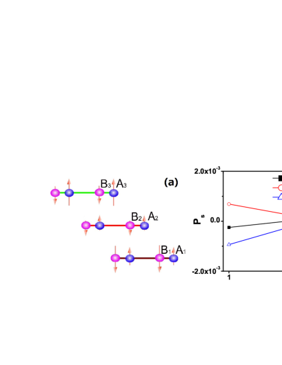
We now discuss the spin density state and the spin polarization of the ABC stacking layer. From the self-consistent mean field theory we obtain the site spin polarization on sublattice or , defined as . The calculated spin polarizations are plotted in Fig. 3(b), and the spin structure in the trilayer graphene is schematically illustrated in Fig. 3(a). The spin ordering is antiferromagnetic, where the neighboring spins (intra- or inter- layer) are anti-parallel to each other. However, there is a net spin polarization on the top or bottom layer, so each surface shows ferrimagnetic ordering. The spin polarization is mainly distributed on the two outer surfaces. In each layer, the spin polarizations on sublattices A and B have opposite directions. The net spin polarization is zero in the mid layer, and has opposite sign in the top or bottom layer. There is a symmetry of combined inversion and time reversal: . Note that the average spin polarization of the whole system is zero. For the parameters given in Fig. 3(b), the site spin polarizations in the top layer are about and on sublattices and , respectively, and the net spin polarization is per site in average, which gives a surface magnetization . The weak surface magnetization on the ABC trilayer graphene is in analogy with the ferromagnetic edge states in graphene zigzag ribbon son , in which the density of states of the flat band edge states is divergent, inducing the edge spin polarization in the presence of a weak interaction. The interaction induced gap in graphene zigzag ribbon has been confirmed in a recent STM experiment dai .
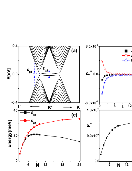
We now discuss graphene layers. For the ABC stacking graphene layers and in the charge neutral case, there is always an interaction () induced gap at the Fermi level with spontaneous surface spin density wave ordering. In Fig. 4(a) and (b), we show the results of layers as an example. Since the minimum band gap () is no longer at the or points as we can see from Fig. 4(a), we introduce the second gap for the energy gap at the or points. As shown in Fig. 4(b), the spin polarization is localized near the surfaces. In Fig. 4 (c), we present the energy gaps as functions of . As increases, first increases to approach its maximum about at , then decreases to a value of at . On the other hand, increases with the layer thickness and reaches a saturated value about . The -dependent spin polarization is shown in Fig. 4 (d), which increases with the layer thickness, and approaches to a saturated value, which is at least 5 to 6 times of the surface magnetization in the trilayer case. Note that the first principle calculations involving a local spin density approximation has been applied to study 8 layers ABC stacking graphene dft , and reported a spin density wave ground state. Their result is consistent with the results of the Hubbard model proposed here, while our results are more general and distinguishes different stacking orders.
We have also applied the mean field theory to study -layer graphene of the ABA stacking. The results are similar to the trilayer case and there is a threshold , which is weakly dependent and remains to be finite at large , the metallic phase is stable against the spin density wave ordering at .
We argue that the mean field theory should give a qualitatively or semi-quantitatively correct physics on the stacking dependent instability, or the insulating or metallic states in layered graphene, while more accurate calculations may refine the estimate of the value of . We remark that the proposed Hubbard model with a moderate should capture the most important physics for the stacking dependent ground states in layered graphene. The intersite Coulomb repulsion has tendency to drive the metallic phase to a charge density wave state, which is not compatible with the on-site studied in the present work. Since the intersite repulsion is relatively weaker than the on-site Coulomb repulsion , we may argue that that term may not be relevant. More exotic states such as quantum spin Hall state and anomalous Hall state have been proposed in models with spin-orbit coupling or intersite interaction on honeycomb lattice sczhang ; kane . The possible realization of these exotic phases in layered graphene will be highly interesting. In view of the very weak spin-orbit coupling in grapheneso , more detailed study will be needed to explore the possibility.
In summary, we have proposed a Hubbard model with a moderate to describe N layer graphene, and applied a mean field theory to study the ground state and the excited energy gap of the charge neutral systems. The ground state of the non-interacting graphene layers are metallic, whose density of states at the Fermi level is divergent as for rhombohedral (ABC) stacking, and is a constant for Bernal (ABA) stacking. The metallic ground state of the ABA stacking layer is stable against the on-site Coulomb repulsion for moderate value of below a threshold about 6-7 eV. The metallic state of the ABC stacking layer is found to be unstable against any repulsion due to the divergent density of states at zero energy. Its ground state is surface antiferromagnetic state with opposite ferrimagnetism on top or bottom surfaces, which opens a gap. The energy gap is estimated to be meV for eV for . Our model and calculations well explain the recent transport experiments, showing that the ABC stacking trilayer graphene is an insulator with a gap about meV, and ABA stacking trilayer graphene remains to be metallic. The spin polarization in the spin ordered state is found to be weak, but should be measurable.
We acknowledge part of financial support from HKSAR RGC grant HKU 701010 and CRF HKU 707010. DHX and YZ are supported by National Basic Research Program of China (973 Program, No.2011CBA00103), NSFC (No.11074218) and the Fundamental Research Funds for the Central Universities in China.
References
- (1) F. Guinea, A.H. Castro Neto, and N.M.R. Peres, Phys. Rev. B 73, 245426 (2006); A.H.C. Neto, F. Guinea, N.M.R. Peres, K.S. Novoselov, and A.K. Geim, Rev. Mod. Phys. 81, 109 (2009).
- (2) S. Latil, and L. Henrard, Phys. Rev. Lett. 97, 036803 (2006).
- (3) H. Min, and A.H. MacDonald, Phys. Rev. B 77, 155416 (2008); F. Zhang, B. Sahu, H. Min, and A.H. MacDonald, Phys. Rev. B 82, 035409 (2010).
- (4) F. Zhang, J. Jung, G.A. Fiete, Q. Niu, and A.H. MacDonald, Phys. Rev. Lett. 106, 156801 (2011); F. Zhang, D. Tilahun, and A.H. MacDonald Phys. Rev. B 85, 165139 (2012).
- (5) A.A. Avetisyan, B. Partoens, and F.M. Peeters, Phys. Rev. B 80, 195401 (2009).
- (6) M. Koshino, and E. McCann, Phys. Rev. B 80, 165409 (2009); M. Koshino, Phys. Rev. B 81, 125304 (2010).
- (7) S.B. Kumar, and J. Guo, Appl. Phys. Lett. 98, 222101 (2011).
- (8) M. Koshino, and E. McCann, Phys. Rev. B 83, 165443 (2011).
- (9) J.-A. Yan, W.Y. Ruan, and M.Y. Chou, Phys. Rev. B 83, 245418 (2011).
- (10) S.B. Kumar, and J. Guo, Appl.Phys. Lett. 100, 163102 (2012).
- (11) T. Wakutsu, M. Nakamura1, and B. Dóra, Phys. Rev. B 85, 033403 (2012).
- (12) M. Otani, M. Koshino, Y. Takagi, and S. Okada, Phys. Rev. B 81, 161403 (2010); M. Otani, Y. Takagi, M. Koshino, and S. Okada Appl. Phys. Lett. 96, 242504 (2010).
- (13) M.F. Craciun, S. Russo, M. Yamamoto, J.B. Oostinga, A.F. Morpurgo, and S. Tarucha, Nat. Nanotechnol. 4, 383 (2009).
- (14) T. Taychatanapat, K. Watanabe, T. Taniguchi, and P. Jarillo-Herrero, Nat. Phys. 7, 621 (2011).
- (15) A. Kumar, W. Escoffier, J.M. Poumirol, C. Faugeras, D.P. Arovas, M.M. Fogler, F. Guinea, S. Roche, M. Goiran, and B. Raquet, Phys. Rev. Lett. 107, 126806 (2011).
- (16) L. Zhang, Y. Zhang, J. Camacho, M. Khodas, and I. Zaliznyak, Nat. Phys. 7, 953 (2011).
- (17) K.F. Mak, J. Shan, and T.F. Heinz, Phys. Rev. Lett. 104, 176404 (2010).
- (18) C.H. Lui, Z.Q. Li, K.F. Mak, E. Cappelluti, and T.F. Heinz, Nat. Phys. 7, 944 (2011).
- (19) Z. Li, C.H. Lui, E. Cappelluti, L. Benfatto, K.F. Mak, G.L. Carr, J. Shan, and T.F. Heinz, Phys. Rev. Lett. 108, 156801 (2012).
- (20) W. Bao, L. Jing, J. Velasco Jr, Y. Lee, G. Liu, D. Tran, B. Standley, M. Aykol, S.B. Cronin, D. Smirnov, M. Koshino, E. McCann, M. Bockrath, and C.N. Lau, Nat. Phys. 7, 948 (2011).
- (21) S.H. Jhang et al., Phys. Rev. B 84, 161408(R) (2011).
- (22) T.T. Heikkil, N.B. Kopnin, and G.E. Volovik, JETP LETT. 94, 233 (2011).
- (23) N.B. Kopnin, T.T. Heikkil, and G.E. Volovik, Phys. Rev. B 83, 220503(R) (2011); N. B. Kopnin, JETP LETT. 94, 81 (2011).
- (24) The small values of longer range hopping integrals do not change the basic conclusion presented here.
- (25) Y.-W. Son, M.L. Cohen, and S.G. Louie, Phys. Rev. Lett. 97, 216803 (2006).
- (26) C.G. Tao, L.Y. Jiao, O.V. Yazyev, Y.-C. Chen, J.J. Feng, X.W. Zhang, R.B Capaz, J.M. Tour, A. Zettl, S.G. Louie, H.J. Dai, and M.F. Crommie, Nat. Phys. 7, 616 (2011).
- (27) S. Raghu, X.-L. Qi, C. Honerkamp, and S.-C. Zhang, Phys. Rev. Lett. 100, 156401 (2008).
- (28) C. L. Kane, and E. J. Mele, Phys. Rev. Lett. 95, 146802 (2005).
- (29) Y. Yao, F. Ye, X. L. Qi, S. C. Zhang, and Z. Fang, 75, 041401(R) (2007).