A gamma- and X-ray detector for cryogenic, high magnetic field applications
Abstract
As part of an experiment to measure the spectrum of photons emitted in beta-decay of the free neutron, we developed and operated a detector consisting of 12 bismuth germanate (BGO) crystals coupled to avalanche photodiodes (APDs). The detector was operated near liquid nitrogen temperature in the bore of a superconducting magnet and registered photons with energies from 5 keV to 1000 keV. To enlarge the detection range, we also directly detected soft X-rays with energies between 0.2 keV and 20 keV with three large area APDs. The construction and operation of the detector is presented, as well as information on operation of APDs at cryogenic temperatures.
keywords:
avalanche photodiode , bismuth germanate , cold neutron , neutron decay , photon detection , weak interactions1 Introduction
A free neutron beta-decays to a proton, electron, and an antineutrino and is predicted to be accompanied by a spectrum of photons with energies up to 782 keV [1, 2, 3, 4, 5], (i.e., ). The photons arise primarily due to inner bremsstrahlung from the high energy electron. Classically, we can think of this process as an electron at rest being rapidly accelerated to its final velocity or imagine that charge is turned on in the same time interval [6]. The first observation of the photons accompanying neutron decay was reported (RDK I) [7] and a detailed analysis determined the branching ratio to be for photon energies between 15 keV and 340 keV [8]. This result is consistent with the theoretical value of for the same photon energy range [9]. The uncertainty in the branching ratio for RDK I was dominated by systematic uncertainties, but these effects are believed to be controllable. Thus to perform a more accurate measurement of the spectrum, higher counting rates are required. A second experiment with an improved detection system was recently performed (RDK II) with the aim of measuring the radiative decay spectrum and branching ratio to 1 % relative uncertainty. The broad improvements in the RDK II experiment were outlined in a previous work [10]. In this paper we describe the construction and operation of the photon detection system in detail.
To provide the context for the description of the improved photon detector, we briefly describe the mode of operation of the experiment; further details can be found in Refs. [8, 10, 11, 12]. The experiments were conducted on the NG-6 neutron beam line[13] at the National Institute of Standards and Technology (NIST) Center for Neutron Research (NCNR) in Gaithersburg, Maryland. A collimated neutron beam (2.5 cm diameter for RDK II) passed along the axis of a 4.6 T superconducting solenoid magnet which is 50 cm long. The high magnetic field ensures that when a neutron decays, the high-energy electron and recoil proton are confined to cyclotron orbits with radii less than 1 mm. At the upstream end of the apparatus, the magnetic field is bent by 9.5 ∘ to guide the charged particles out of the beam and towards a silicon surface barrier detector (SBD). (In this paper we use the terms “downstream”and “upstream” to refer to the directions parallel and antiparallel to the neutron velocity vector.)
In the RDK I experiment, a single 12 mm by 12 mm by 200 mm bar of bismuth germanate (BGO) was coupled to a large-area avalanche photodiode (APD) and placed at the bottom of the magnet bore, along the length, and just outside of the neutron beam. The strong magnetic field inside the bore precluded the use of photomultiplier tubes (PMTs), whereas at the time we began this work APDs had been reported to be insensitive to magnetic fields [14]. The detector operates near liquid nitrogen temperature, which substantially decreases the noise in the APD and increases its gain, and increases the light output of the BGO crystals [15, 16].
A candidate radiative decay event is identified in software by requiring the correlation of a prompt electron signal in the SBD, a simultaneous photon signal in the photon detector, and a delayed, low-energy proton pulse in the SBD. Hence accurate determination of the timing of the photon signal with respect to the electron signal is important for rejection of background photons. Digitizing the preamplifier pulses, rather than simply counting events using a spectroscopy amplifier with discrimination, allowed for optimized timing as well as off-line analysis of the photon signal waveforms after the experiment. The temporal resolution has been improved by about a factor of two compared to the results in Ref. [12] by improved light collection, electronics, and signal-to-noise ratio.
To improve upon the RDK I experiment, a twelve element detector was constructed to increase the solid angle for photon detection. In addition the range was extended down to 0.2 keV using three larger APDs for direct detection of soft X-rays. In the course of developing this direct detector we found that the response of the APDs employed is strongly distorted when operated at cryogenic temperatures with a strong magnetic field in the APD plane[17]. In Sec. 2 we describe the RDK II photon detector and in Sec. 3 we present its performance. Several features of operating the BGO crystals and APD detectors near liquid nitrogen temperature are presented in Sec. 4.
2 Photon Detection System
In this section, we provide general motivations for the construction of the RDK II photon detector, followed by a detailed description of the construction.
2.1 General considerations
Due to the long neutron lifetime (15 min) and the relatively low intensity of neutron beams, the detection rate of electron/delayed proton coincidences in the RDK II apparatus was only 10 s-1. Due to the low branching ratio for neutron radiative decay, a large solid angle for detection is desired. The photon emission rate increases rapidly with decreasing photon energy, so obtaining a low detection threshold is also desirable. High resolution is not required because the neutron radiative decay produces a smooth, featureless spectrum of photons similar to that of external bremsstrahlung.
Whereas doped inorganic crystals generally exhibit lower light yield at 80 K relative to room temperature, the yield from pure inorganic crystals increases at low temperature [15, 16]. As discussed elsewhere [12], both pure CsI and BGO were investigated; BGO was chosen because pure CsI is hygroscopic, exhibited greater spatial dependence in the light yield, and yields a higher probability of Compton scattering. The RDK II detector consists of an annular array of twelve 12 mm by 12 mm by 200 mm [18, 19] BGO bars that surrounds the cold neutron beam. To maximize the solid angle, we briefly considered a single annular BGO crystal coupled to APDs, but this results in substantially decreased light collection. For the relatively low gain of APDs compared with PMTs, such light loss is unacceptable. For a 12 mm path length, BGO has nearly 100 % absorption below 200 keV, decreasing to 50 % at 900 keV [18]. The BGOs were placed in mechanical contact with large-area APDs with no additional optical coupling. The 13.5 mm 13.5 mm active area of each APD [20] was slightly larger than the end face of each BGO crystal to ensure full coverage of the crystal and facilitate alignment between the APD and BGO crystal. To conserve physical space and avoid failure due to thermal stress upon cooling, these APDs lacked the typical protective outer casing. Nevertheless, the APDs proved to be rugged and did not suffer from direct contact with the hard surfaces of the BGO crystals.
2.2 Mechanical Setup
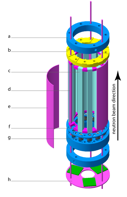
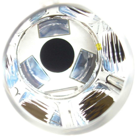
The BGO crystals and APD detectors are mounted in a low-mass, non-magnetic mechanical structure, which fits into the bore of the magnet. A schematic view of the system is shown in Fig. 1 and a photograph of the partially disassembled system is shown in Fig. 2.
The BGO crystals are positioned at 30 ∘ intervals and at a radius of 36 mm (inside of crystals) by two aluminum rings with cutouts to define their position. The crystals are held in place lengthwise by non-metallic rings at both ends. Spring-loaded pistons in the nylon ring (upstream) ensure that contact between the BGO crystals and the APDs is preserved when the apparatus is cooled. The G10 ring (downstream) provides spaces for the APD detectors (see right side of Fig. 2). Three 120∘ sections of an aluminum cylinder (1.65 mm wall thickness) constrain the crystals to their slots and are thermally connected to the magnet’s liquid nitrogen reservoir. Fig. 2 shows the APD holder ring on the right, with the APDs facing away from the viewer and the electrical contacts with wiring visible.
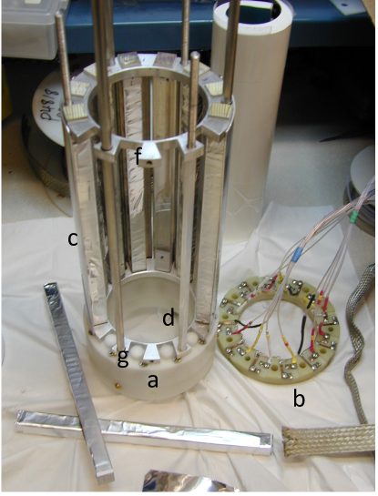
The detector package is designed so that it can be radially adjusted by up to 3 mm in order to center it with respect to the beam. Three brass adjusters with hemispherical heads (to reduce thermal contact) were placed radially within each nylon ring, and each was translated with a stainless steel rod. Fig. 2 shows a brass foot extending from the bottom-left nylon ring with its corresponding adjustment rod.
Four silicon diode temperature sensors [21] are used to monitor the temperatures at the upstream and downstream ends of the detector package as well as on the liquid-nitrogen and liquid-helium-cooled magnet surfaces. To block background gamma rays from the reactor and possible correlated bremsstrahlung radiation from the SBD, a small Pb block was placed just upstream of the single BGO bar used In the RDK I experiment. In RDK II, a 2.5 cm thick Pb annulus was employed, with 1.8 mm thick copper added to absorb secondary Pb X-rays (72 keV to 80 keV).
| far end | long | |
|---|---|---|
| - | Al foil or Al-Mylar | 1.05 |
| Al foil | - | 1.6 |
| PTFE | - | 1.8 |
| paint | 10 mm painted | 2.0 |
| paint | - | 2.2 |
| roughened, paint | - | 1.8 |
2.3 Light Collection
To maximize the BGO light output, we investigated an optical coupler between the BGO crystal and the APD and covering or treating the BGO surfaces to increase the amount of light that reaches the APD. Light transmission between the BGO crystal and APD can be improved by providing a medium with an index of refraction between =1 and =2.15 (BGO), where we have assumed there is a microscopic gap between the BGO crystal and the APD. Operation at cryogenic temperatures precluded the use of optical grease and other options, but the use of silicone rubber sheet has been reported for temperatures as low as 20C [23]. We studied the coupling of BGO to APD with silicone rubber (GE RTV615; =1.406 [24]). According to Monte Carlo simulations, this optical coupler should increase the amount of light extracted from the BGO crystal by a factor 2.3. However, we found that optical contact was lost for tests near liquid nitrogen temperature, thus yielding no improvement in light collection. We expect that the difference in thermal contractions of the crystal, the hardened silicone rubber, and the APD is responsible for this loss of contact. While it might be possible to find a suitable optical coupler, this method was not pursued any further. Thus the present detector has an n=1.0 gap between the BGO crystals and APDs.
Studies were made of different methods of covering or treating the BGO detector surfaces to optimize light collection. For convenience these tests were performed at room temperature using the 662 keV gamma-ray from a 137Cs source to illuminate the BGO crystal near its center. A PMT, separated from one of the crystal surfaces by an air gap, was used to detect the scintillation signals. Our results are summarized in Table 1.
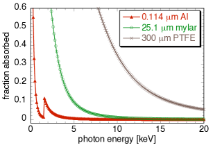
The results are consistent with expectations from Ref. [25]. A diffuse reflector on the far end increases light collection by redirecting some otherwise trapped light into the angular cone which allows light to escape the crystal towards the PMT. Light which can escape towards the PMT internally reflects from the long surfaces, therefore applying diffuse paint on those surfaces reduces light collection in the PMT. We decided to paint the far ends of each BGO crystal with reflective paint and to loosely cover the remaining detector with reflective foil, mainly for mechanical and external light-intrusion protection. Specifically, the long sides of each BGO crystal were covered by two layers of aluminized Mylar (total of 12.4 m Mylar and 0.065 m aluminum). An additional aluminized Mylar sheet (12.7 m Mylar and 0.049 m aluminum) separated the beam from the BGO crystals. The long-side regions near the end faces (12 mm) had additional layers of PTFE tape and aluminized Mylar for mechanical protection from the metal positioning rings (300 m PTFE and 6 m Mylar with 0.033 m aluminum).
The covering on the BGOs was deliberately kept thin to reduce absorption of low energy photons and thus help minimize the energy detection threshold for the experiment. Absorption curves for the cover materials used are shown in Fig. 3. As shown, the absorption of aluminized Mylar and PTFE decrease to less than 5 % above 6.5 keV and 21 keV, respectively.
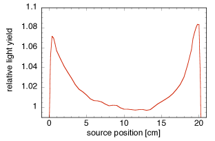
Ref. [25] also predicts for our configuration (a photon detector coupled via an n=1 gap to the crystal, diffuse reflector on opposite end) that the detected light yield for uniform light creation depends on the location along the length of the crystal. Indeed we found that the detected light created with collimated sources increases at both ends, near the APD and near the far end (Fig. 4).
During initial design we considered using APDs on both crystal ends, but rejected this approach due to increased cost and additional complexity in construction and data acquisition. We later found that diffusely reflecting paint on the far end yielded an improvement in light collection comparable to what would be expected for APDs at both ends.
2.4 High voltage and signal processing
The electrical ground and high voltage (HV) connections (which also carry the APD signals) were provided by PTFE-tube insulated 32 AWG (American Wire Gauge, 0.20 mm diameter) phosphor-bronze wires within the magnet’s vacuum chamber. These thin wires were chosen over coaxial cables to minimize heat load and outgassing. Although these signal/HV cables were not shielded and shared ground wires in groups of four, cross talk was found to be less than 0.5 % of signal amplitude.
Outside of the magnet, cabling continued via 30 cm long double-shielded RG-59 cables to Canberra 2006 preamplifiers [26]. Double shielding the coaxial HV/signal cables between the vacuum feedthrough and preamplifier reduced low-amplitude noise considerably. The preamplifier output signals were directly fed into two 8-channel GaGe cards [27], which were set to digitize the signals with 40 ns/channel resolution in 80 s long traces. The decay time constant of the preamplifiers is 50 s. Because the gain of the APDs is highly sensitive to the high voltage, we employed power supplies [28] that could be set in 0.1 V steps (5 % gain change for 1 V change). Details of gain dependencies are described in Sec. 4.2. The APD gain was found to be stable to 1 %, and gain drifts could be correlated with drift in the temperature as determined from the silicon diode temperature sensors.
2.5 Direct soft X-ray detector
Soft X-rays from neutron radiative decay with energies between 0.2 keV and 20 keV were directly detected with additional APDs [10]. The detector, shown in Fig. 5, consisted of three 28 mm by 28 mm (active area) APDs [20] mounted around the neutron beam with the plane of the APD perpendicular to the magnetic field. This configuration was chosen because we found significant distortion of the APD response when the plane of the APD was parallel to the magnetic field (and thus the APD electric field was perpendicular to the magnetic field) [17]. In the configuration shown in Fig. 5 the only effects of the magnetic field for tests with 5.9 keV X-rays provided by an 55Fe source were a small (less than 10 %) decrease in the gain and a decrease of up to a factor of two in the width of the peak. A 55Fe source was mounted near the APDs to provide a continuous energy calibration during the experiment. The APDs were read out with the same preamplifier and GaGe card configuration as for the APDs in the scintillator detector.
3 Performance
3.1 BGO/APD scintillator detector

Signals from the BGO/APD detector are shown in Fig. 6 for 300 keV and 12 keV photons that were recorded during the radiative decay experiment; the energy calibration was determined from 511 keV gamma-rays from electron-positron annihilation that were present in the background spectrum. The peak-to-peak noise corresponds to a minimum detectable photon energy of 5 keV. The 5 s rise time is governed by the time scale for scintillation in the BGO crystal, which increases substantially at low temperatures [29].
To test the detector response with radioactive sources, we employed a reentrant tube that allowed the sources to be outside the magnet’s vacuum chamber while illuminating the detector in a similar way as the photons from neutron decay. Pulse height spectra for tests of the BGO/APD detector with 137Cs, 133Ba, 57Co, and 241Am sources are shown in Fig. 7, along with the results of modelling the detector response based, in part, on MCNP5 [30] predictions for the energy deposit spectrum in each BGO crystal. The experimental results are being used to test this modelling, which is required for analysis of the neutron radiative decay experiment. A more detailed treatment will be described in a future publication. Although nonlinearity in the response of BGO has been reported[31, 32, 33, 34] the modeling shown in Fig. 7 assumes a linear response. We are currently investigating the magnitude of nonlinearity in the overall detection system for our experimental operating conditions.
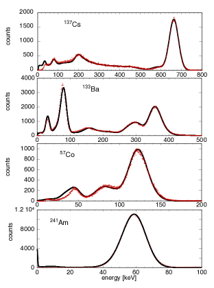
The typical energy resolution is 10 % FWHM (full width at half maximum) at 662 keV and 30 % at 60 keV, dominated by the statistics of electron-hole generation and multiplication in the APD [35]. The observed resolution is close to the value of 11 % that we estimate using a typical excess noise factor of 2.5 [36, 37] and 1000 photoelectrons expected for a 662 keV gamma ray, where we have assumed a photon yield for BGO of 24 keV-1 [32], a photon collection efficiency of 10 % (based on Ref. [25] and Monte Carlo simulations), and a quantum efficiency of 70 % [38] for the green BGO fluorescence (peak at 530 nm at 90 K [15]).
3.2 Direct soft X-ray detection


Fig. 8 shows APD signals after the preamplifier for a 5.9 keV X-ray from the 55Fe source and a signal with a amplitude corresponding to a 0.5 keV X-ray; the latter was obtained during the neutron decay experiment. The rise time of the signal from the soft X-ray detector is much faster than those of the scintillator detector. The peak-to-peak noise corresponds to a minimum detectable photon energy of 0.2 keV. Fig. 9 shows the typical pulse height spectrum from the APD for 5.9 keV X-rays from a 55Fe source. At high magnetic field the typical resolution for the response to 5.9 keV X-rays was 15 % FWHM.
Between 1 keV and 5 keV, X-rays are detected by APDs with close to 100 % efficiency [39]. Above 5 keV, the detection efficiency decreases due to decreasing absorption by silicon. For the 60 m depletion layer for the APDs employed, the detection efficiency decreases by an order of magnitude between 5 keV and 16 keV. Primarily below 1 keV but also just above the Si K-edge at 1.8 keV, there are changes in the pulse height spectrum arising from the short penetration depth into the silicon coupled with strong doping at the front of the APD. In addition, there is increased absorption from the protective glass layer on the APD. The complex response in the 0.35 keV to 1.5 keV range has been studied by measurements with monochromatic X-ray beams and synchrotron radiation [40]. As the X-ray energy is reduced below 1 keV, an increasing fraction of events that have incomplete collection of photoelectrons was observed. For two of the three APDs used in the neutron experiment, the detection efficiency for our experimental threshold was found to decrease by an order of magnitude between 1.0 keV and 0.4 keV. For the third APD (from a different wafer) the low energy response was improved, which we presume is due primarily to a shallower depth of doping.
4 Cryogenic Features of APDs
Aspects of cryogenic operation of APDs have previously been reported [36, 41]. During testing and operation of the detector at cryogenic temperatures, we observed several features that were important for the performance of this experiment. These features were studied in the BGO/APD detectors, but should dominantly represent APD properties and not properties of the BGO crystals. Although the features described here have only been explored for the APDs used [20], they may serve as a guide of what to expect and what to look for when operating APDs at cryogenic temperatures.
The gain of a given APD depends strongly on the magnitude of the applied high voltage () and temperature. In addition we observed some dependence on magnetic field strength, as previously noted (see Sec. 2.5). Furthermore we observed a dependence on how much time has elapsed since the high voltage has been applied, and the size of this effect varied with temperature
4.1 Operating high voltage
At low temperatures, e.g., near liquid nitrogen temperatures, one can define a limiting “breakdown high voltage”, , within 1 V. At this voltage, noise signals (best observed without a radioactive source) increase in amplitude so that they saturate a preamplifier. Within 3 V above the bias current, normally below 1 nA, increases to more than 10 nA. No damage to the APDs was observed even for up to 100 V above for several seconds. In this experiment ranged from 1387 V to 1479 V for the twelve APDs operating at 86 K.
The gain-to-noise ratio has a broad maximum in the range of about 20 V to 50 V below . The absolute gain of an APD at a given voltage below breakdown in this range depends on the individual APD; for the 12 detectors of this experiment at 90 K the observed signal amplitudes for a given photon energy absorbed in the BGOs varied by up to a factor of 2.1 at V, where is the voltage below breakdown.
4.2 Gain dependence
Figure 10 shows the variation of gain with for two detectors. At V we find the gain changes of (4.0 0.7) %/V, where the uncertainty represents one standard deviation. We found that the observed gain can be approximately predicted in terms of :
| (1) |
The result of dividing the experimental gain by is shown in Fig. 10 by the open symbols. While this empirical parameterization is not perfect for all detectors, it allows one to predict the gain by better than a factor of two over the range where the gains change by about a factor of 30.
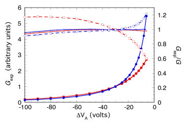
If one allows for an offset in , , then one can obtain a nearly perfect gain prediction, as can be seen by observing the dotted lines in Fig. 10, which show the experimental gain divided by .
Based on slow warm-up tests of the BGO/APD detectors between 90 K and 110 K, we found that the signals decreased by between 5 %/K and 8 %/K and the breakdown voltage increased by between 1 V/K and 1.5 V/K for the group of detectors employed. The observed gain changes originate mainly from the temperature dependent APD gains, as the BGO light output decreases 1 %/K near 100 K [16].
A variation in gain was observed with magnetic field for the field perpendicular to the plane of the APD. For the BGO/APD detectors at 80 K the gain for tests with the 662 keV line from the 137Cs source varied by 5 % to 30 %, depending on detector, when the magnetic field was increased from zero to 4.6 T. The gain shift was roughly proportional to the magnetic field. There was no obvious correlation between the sign or magnitude of the gain shift and the orientation of the detectors around the magnet’s axis (the angle increases in steps of 30 degrees with increasing detector number).
4.3 APD gain recovery delay after HV cycling
At cryogenic temperatures we found that turning the APD HV off and immediately back on (“cycling the HV”) did not restore the gain immediately, as is the case at room temperature. Indeed, it may take days for the gain to fully recover even after shut down for only one second.
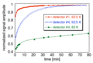
Fig. 11 demonstrates this effect for two detectors, labeled detector #1 and detector #4, at a temperature of 92.5 K. Four other APDs from the same purchase behaved similarly to detector #4, but we also show data for detector #1, for which the effect was less pronounced, that was from a later purchase. The data are normalized to unit signal amplitude at long times after HV cycling.
The data for all APDs tested were well fit by a double exponential form given by , where , , , and are adjustable parameters. Typical values (see Table 2) were between 1.6 min and 2.6 min for the short time constant and between 14 min and 17 min for the long time constant .
| temperature | ||
|---|---|---|
| 82 K | 5 min | 330 min |
| 93 K | (1.6 to 2.6) min | (14 to 17) min |
| 115 K | - | 5 min |
The pre-power-cycling gain value and several-hour-delayed “steady-state” gain values differ by nearly two percent. The origin of this gain change has not been investigated; it may indicate a separate very-long-term gain drift or a hysteresis effect from having turned on the HV originally at a different temperature.
The gain recovery time constant depends strongly on the temperature of the APDs. This is apparent from the very slowly rising gain recovery curve taken at 82 K, also shown in Fig. 11. At this temperature we obtained =5 min and =330 min, but we note that the double exponential form is purely phenomenological and we did not take data for the many hours that would be required to follow the recovery at 82 K. In contrast, at 115 K (data not shown) was measured to be less than 5 min.
The origin of these effects is not understood, but could be due to increased time to establish the depletion region upon cycling the HV. As expected, the gain recovery effect was also observed in the larger APDs for direct detection of 5.9 keV X-rays from the 55Fe source. Hence the effect is apparent for both optical and direct soft X-ray detection. During the radiative decay experiment the bias for the APDs was turned on before cooling the APDs and left on for the entire time the apparatus was at cryogenic temperatures. It is possible that not far below 80 K the APDs become unusable after HV cycling due to months-long recovery times. However, applying HV first and then cooling the detectors may be feasible. It is noteworthy that, at the temperatures studied, reducing the HV by only a few hundred volts did not show the delay in gain recovery. This could imply that after cooling to well below 82 K with the HV already applied at higher temperatures it may still be possible to vary the APD gain by changing the HV.
5 Summary
For an experiment to detect the photons that accompany neutron beta decay, a compact photon detector was constructed that could operate in high magnetic field and near liquid nitrogen temperature. The scintillator/APD detector operates from a low energy threshold of 5 keV to 1000 keV. A large solid angle for detection was obtained by using long BGO crystals assembled in a tight cylindrical configuration. The scintillation light was read out by APDs. The low energy detection threshold was achieved by operating the BGO crystals and the APDs near liquid nitrogen temperatures, by minimizing the amount of detector-covering materials, and by minimizing noise pickup. BGO light extraction studies found improved performance by selectively applying diffuse reflective paint. Large sensitivity gains may be possible by better optical coupling of APDs to BGOs, but no suitable cryogenic coupling agent was found. The mechanical design optimizes the solid angle coverage while fitting into the limited space (117 mm diameter) of the bore of a superconducting solenoidal magnet without compromising the capability of precise detector alignment around an axial neutron beam. The detection range was increased to include 0.2 keV to 20 keV by directly detecting soft X-rays with APDs.
During testing and operation of the detector system several noteworthy properties of the APD detectors, relevant at cryogenic temperatures, became apparent which may be important to consider when planning cryogenic APD operations. Besides the known properties of strong sensitivity to temperature and bias voltage, we observed pronounced delays in achieving steady-state gains when cycling the bias; this delay rapidly increases with falling temperature and may approach several months below about 70 K.
ACKNOWLEDGEMENTS
We thank R. Farrell for numerous discussions about APD operation and properties and L.T. Hudson and R.M. Lindstrom for critical reading of the manuscript. This work was supported in part by the Department of Energy and the National Science Foundation.
References
- [1] Y. V. Gaponov, R. U. Khafizov, Physics of Atomic Nuclei 59 (1996) 1213.
- [2] Y. V. Gaponov, R. U. Khafizov, Phys. Lett. B 379 (1996) 7.
- [3] Y. V. Gaponov, R. U. Khafizov, Nucl. Instrum. Meth. A 440 (2000) 557.
- [4] V. Bernard, S. Gardner, U.-G. Meißner, C. Zhang, Phys. Lett. B 593 (2004) 105.
- [5] V. Bernard, S. Gardner, U.-G. Meißner, C. Zhang, Phys. Lett. B 599 (2004) 348.
- [6] J. D. Jackson, Classical Electrodynamics, 3rd Ed., Wiley, New York, 1998.
- [7] J. S. Nico, et al., Nature 444 (2006) 1059.
- [8] R. L. Cooper, et al., Phys. Rev. C 81 (2010) 035503.
- [9] S. Gardner, private communication (2006).
- [10] R. L. Cooper, et al., Nucl. Instrum. Meth. A 611 (2009) 219.
- [11] R. Cooper, The radiative decay mode of the free neutron, Ph.D. thesis, University of Michigan (2008).
- [12] T. R. Gentile, et al., Nucl. Instrum. Meth. A 579 (2007) 447.
- [13] M. Dewey, et al., J. Res. Natl. Inst. Stand. Technol. 241 (2005) 213.
- [14] M. Boucher, et al., Nucl. Instrum. Meth. 505 (2003) 136.
- [15] H. V. Piltingsrud, J. Nucl. Med. 20 (1979) 1279.
- [16] J. Gironnet, et al., Nucl. Instrum. Meth. A 594 (2008) 358.
- [17] T. R. Gentile, C. D. Bass, J. S. Nico, H. Breuer, R. Farrell, Nucl. Instrum. Meth. A 652 (2011) 520.
- [18] Saint-Gobain Crystals, 17900 Great Lakes Parkway, Hiram, OH 44234-9681 USA; www.detectors.saint-gobain.com. Certain trade names and company products are mentioned in the text or identified in an illustration in order to adequately specify the experimental procedure and equipment used. In no case does such identification imply recommendation or endorsement by the National Institute of Standards and Technology, nor does it imply that the products are necessarily the best available for the purpose.
- [19] Rexon Components, Inc., 24500 Highpoint Rd., Beachwood, OH 44122.
- [20] Model 1315-P (BGO) and Model 2853-P (soft X-ray), Radiation Monitoring Devices, Inc., 44 Hunt Street, Watertown, MA 02472, USA.
- [21] Model Si-410, Scientific Instruments, Inc., 4400 West Tiffany Drive West Palm Beach, Florida 33407.
- [22] See http://henke.lbl.gov/optical_constants/filter2.html.
- [23] T. Ikagawa, et al., Nucl. Instrum. Meth. A 538 (2005) 640.
- [24] MG Chemicals, 9347 - 193rd Street, Surrey, B.C., Canada, V4N 4E7; http://www.mgchemicals.com/products/615.html.
- [25] G. Keil, Nucl. Instrum. Meth. 89 (1970) 111.
- [26] Canberra Model 2006 Proportional Counter Preamplifier, Canberra Industries, 800 Research Parkway, Meriden, CT 06450.
- [27] Gage CompuScope 8289 (Octopus 12-bit CompuScope A/D card: 125 MS/s per channel, 8 channels, 128 MS memory), DynamicSignals LLC, 900 N. State St., Lockport, IL 60441.
- [28] Model NHQ222M, iseg Spezialelektronik GmbH, Bautzner Landstra e 23 D-01454 Radeberg / OT Rossendorf, Germany; www.iseg-hv.com.
- [29] M. Weber, R. Monchamp, J. Appl. Phys. 44 (1973) 5495.
- [30] F. B. Brown, et al., a General Monte Carlo N-Particle Transport Code, Version 5 LA-UR-03-1987 (2003).
- [31] P. Dorenbos, J. T. M. de Haas, C. W. E. van Eijk, IEEE Trans. Nucl. Sci. 42 (1995) 2190.
- [32] M. Moszynski, et al., IEEE Trans. Nucl. Sci. 51 (2004) 1074.
- [33] M.-A. Verdier, et al., Phys. Rev. B 84 (2011) 214306.
- [34] I.V. Khodyuk and P. Dorenbos, http://arxiv.org/abs/1204.4350.
- [35] M. Moszynski, M. Szawlowski, M. Kapusta, M. Balcerzyk, Nucl. Instrum. Meth. A 497 (2003) 226.
- [36] M. Moszyński, et al., IEEE Trans. Nucl. Sci. 49 (2002) 971.
- [37] L. Ludhova, et al., Nucl. Instrum. Meth. A 540 (2005) 169.
- [38] M. McClish, et al., IEEE Trans. Nucl. Sci. 53 (2006) 3049.
- [39] R. Farrell, K. Vanderpuye, G. Entine, M. Squillante, IEEE Trans. Nucl. Sci. 38 (1991) 144.
- [40] T. R. Gentile, M. Bales, U. Arp, B. Dong, R. Farrell, Rev. Sci. Instrum. 83 (2012) 053105.
- [41] L. Yang, et al., Nucl. Instrum. Meth. A 508 (2003) 388.