Temperature dependence of the electronic structure and Fermi-surface reconstruction of Eu1-xGdxO through the ferromagnetic metal-insulator transition
Abstract
We present angle-resolved photoemission spectroscopy of Eu1-xGdxO through the ferromagnetic metal-insulator transition. In the ferromagnetic phase, we observe Fermi surface pockets at the Brillouin zone boundary, consistent with density functional theory, which predicts a half metal. Upon warming into the paramagnetic state, our results reveal a strong momentum-dependent evolution of the electronic structure, where the metallic states at the zone boundary are replaced by pseudogapped states at the Brillouin zone center due to the absence of magnetic long-range order of the Eu moments.
pacs:
74.25.Jb, 79.60.-i, 71.30.+h, 75.47.LxEuO exhibits a remarkable array of magnetic properties which are induced by carrier doping, including colossal magnetoresistance () shapira1973 , a large metal-insulator transition () petrich1971 ; penney1972 , spin polarized carriers () steeneken ; schmehl2007 , and an enhancement of the Curie temperature () shafer1968 . Based on these properties and its compatibility with Si, GaN schmehl2007 , and GaAs swartz , doped EuO has recently attracted attention to its potential in the development of spin valves and polarized injectors for spintronics santosPRB . Despite nearly 40 years of research, a definitive picture of the momentum-resolved electronic structure of doped EuO across the metal-insulator transition is still lacking, in part due to the strong Coulomb repulsions in the half-filled Eu shell which pose a challenge for calculations. Here we utilize angle-resolved photoemission spectroscopy (ARPES) to investigate epitaxial Eu1-xGdxO thin films across the metal-insulator transition. Our measurements reveal a striking dichotomy of the behavior of doped carriers in momentum space which evolve between a delocalized, spin-polarized band at the Brillouin zone (BZ) boundary in the ferromagnetic (FM) metallic state, to localized, pseudogapped states at the BZ center in the paramagnetic (PM) state.
35 nm thick Eu1-xGdxO films were grown in both Veeco 930 and Veeco GEN10 oxide molecular-beam epitaxy (MBE) chambers on (110) terminated YAlO3 substrates in adsorption-controlled conditions at a temperature of 350 ∘C ross ; sutartoGd , where stoichiometric EuO can be produced without detectable concentrations of oxygen vacancies. The Eu flux was atoms/cm2s, and the Gd flux was varied to achieve different doping levels (). Immediately following growth, the films were transferred to the ARPES chamber in less than 300 seconds under ultra-high vacuum ( torr). ARPES measurements were performed using a VG Scienta R4000 spectrometer, with an instrumental energy resolution meV, He I photons ( = 21.2 eV) and a base pressure typically better than torr. Film quality was monitored during growth using reflection high-energy electron diffraction (RHEED) and after ARPES measurements using low-energy electron diffraction (LEED), which shows a surface structure. Results were confirmed by repeating measurements on over 35 individual samples and temperature-dependent measurements were confirmed by cycling samples from 140 K to 10 K and back to 140 K without noticeable degradation. Fermi surface (FS) maps were verified on multiple samples to check against the possibility of degradation. Additional ex situ characterization was performed on films capped with amorphous Si using x-ray absorption spectroscopy at the SGM beamline at the Canadian Light Source to determine the true Gd concentration and x-ray diffraction to verify the film structure and phase purity supplemental .
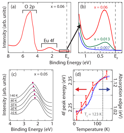
In Fig. 1(a), we show the valence band for Eu0.94Gd0.06O with a nominal of 123 K, which consists of O states between 4-6 eV and Eu states around 1-3 eV binding energies, consistent with measurements on single crystals eastman and undoped EuO films miyazaki . In Fig. 1(b), we show the near spectra for = 0.007, 0.013, and 0.06 doped samples at 10 K, exhibiting a monotonic increase in spectral weight with Gd (electron) doping. Films with were highly insulating, did not exhibit near spectral weight, and charged up electrostatically upon exposure to the photon beam; we could not observe evidence of metallic surface states predicted for undoped EuO schillerPRL . Shown in Fig. 1(c) is the temperature dependence of the peak in Eu0.95Gd0.05O around , which shifts to lower binding energies as the sample is cooled below (also reported by Miyazaki et al. miyazaki ), while its lineshape remains largely unchanged. The temperature-dependent shift of the peak maximum is in close agreement with the optical redshift for a bulk sample of similar carrier concentration schoenes shown in Fig. 1(d), indicating that our ARPES measurements are consistent with bulk properties measured using optical absorption.
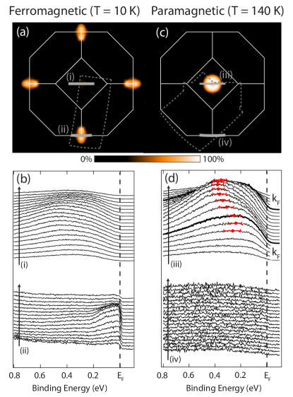
In order to address the nature of the spin-polarized metallic carriers in the FM state, we focus on the near states at 10 K and will discuss the data above later in the text. A Fermi surface (FS) map is shown in Fig. 2(a). The map clearly exhibits small elliptical pockets centered around the point ((0, 2) in the 2D BZ) at the zone boundary. A perpendicular cut through this pocket in Fig. 2(b) reveals an electron-like band with a sharp Fermi cutoff at , indicating metallic states. Additionally, we also observe a low energy feature located near the point ((0, 0) in the 2D BZ), shown in Fig. 2(b). We attribute these to more deeply bound states (DBS) which are likely defect-derived and centered at a binding energy of 0.45 eV and exhibit only very weak dispersion and no appreciable spectral weight at , and therefore are not visible in the FS map.
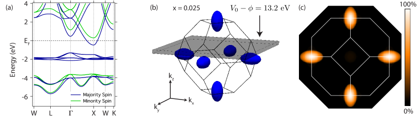
In Fig. 3, we compare our low temperature ARPES results to electronic structure calculations for Eu1-xGdxO. The calculations were performed using density functional theory (DFT) with the generalized gradient approximation plus on-site Coulomb interactions (GGA+U), based on the parameters determined by Ingle and Elfimov ilya ; supplemental . In Fig. 3(a), we plot the band structure along high symmetry lines, showing the minimum of the spin-polarized conduction band at the point. To treat the effect of carrier doping in the simplest manner possible, we perform a rigid shift of the chemical potential into the conduction band. Fig. 3(b) shows the calculated 3D FS consisting spin-polarized electron pockets centered around . In Fig. 3(c), we present a simulated ARPES FS intensity map for which takes into account the three-dimensionality of the FS using an inner potential of , where is the work function miyazaki . We describe the treatment of the three-dimensionality of the electronic structure as well as ARPES measurements taken at a different photon energy (He II, = 40.8 eV) in further detail elsewhere supplemental , and will return to discuss our choice of the doping level later in the text. The predicted ARPES FS is composed of spin-polarized, elliptical electron pockets centered at (0, 2) of primarily Eu character. Although this is a simplified approach, the calculated FSes nevertheless appear to capture qualitatively the FS features experimentally observed in Fig. 2(a).
The qualitative agreement between the simulation and experiment demonstrates that DFT based approaches ilya ; schillerSSC can accurately treat the mobile carriers in the FM metallic state. This finding supports the numerous theoretical studies of EuO, including the possible effects of epitaxial strain on ilya , realizing a new multiferroic from strained EuO bousquet , and predictions for spin-polarized 2D electron gases at the interfaces of EuO-based superlattices Wang . This agreement can also be taken as supporting evidence that the FM metal-insulator transition arises from an indirect exchange interaction between the Eu conduction band and the FM ordered Eu moments which lowers the bottom of the majority spin conduction band below .
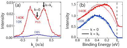
The more localized DBS states near (0, 0) are beyond the scope of our simple rigid band approximation. The DBS states exhibits some momentum dependence, indicating that these states comprise a defect band which is not completely localized in real space. Nevertheless, due to their vanishing spectral weight at , shown by the momentum distribution curve (MDC) in Fig. 4(a), the DBS likely play a negligible role in the low temperature conductivity, which is dominated by the metallic states at (0, 2).
Upon warming into the PM insulating state (140 K), the FS map changes dramatically (Fig. 2(c)). Around (0, 2), the metallic states are lifted above (shown in Fig. 2(d) and the Supplemental Material supplemental ) due to the vanishing FM exchange splitting. Spectral weight is transferred to the BZ center, contributing to the ring of intensity around (0, 0), also shown in Fig 2(d). The contrast between the behavior of carriers at (0, 0) versus at (0, 2) underscores the importance of employing a momentum-resolved probe in studying the properties of carrier doped EuO.
Our comparison of the lineshape at the BZ center below and above shown in Fig 4(b) and in the Supplemental Material supplemental shows that the DBS (10 K) consist of broad and only weakly dispersive spectral weight. In contrast, while the spectra above also exhibit the broad signature of the DBS at higher binding energy, they show an additional more highly dispersive component of spectral weight which sits closer to , indicating that another population of carriers has formed between the DBS and , which we call the pseudogapped states (PGS). The small but finite spectral weight of the PGS near is likely responsible for the transport properties observed in the PM phase for films in this doping regime, which exhibit “bad metal” conduction at high temperatures, followed by a slight exponential upturn in the resistivity above , indicating the formation of a small (10 meV) activation gap mairoserDiplomaThesis ; matsumoto . Such a gap is much smaller than our combined instrumental ( meV) and thermal broadening at 140 K and therefore cannot be detected in our measurements. This activated behavior in Eu1-xGdxO is notably different from the variable range hopping conduction observed in the similar ferromagnetic metal-insulator compound Ga1-xMnxAs sheu .
Despite the increased intensity near , the PGS are still broad in energy and strongly suppressed in intensity within 200 meV of , forming a pseudogap reminiscent of features seen in the high- cuprates Shen1 , Fe3O4 schrupp , and the manganites mannella ; dessau , all of which exhibit insulating behavior resulting from strong electron correlations. For the case of Eu1-xGdxO, such pseudogapped behavior could arise from incoherent carrier hopping due to an indirect exchange interaction between the dopant electrons and the randomly fluctuating background of Eu spins above . The spectral weight transfer that we observe through the metallic transition is related to the transferring of electrons from the PGS to spin-polarized electron pockets at the BZ boundary. This non-trivial behavior is unexpected and demonstrates that doped electrons in EuO do not simply enter non-dispersive donor impurity states.
Our observation of two populations of carriers above is consistent with the recent Hall measurements by Mairoser et al. mairoser which indicate that less than 50 % of the Gd dopants are electrically active at 10 K. The PGS electrons which are closer to are electrically active above and are transferred to the EuO conduction band below . On the other hand, the electrons comprising the DBS well below appear to remain inactive at all temperatures. By integrating the spectral weight around (0, 0) from -1.0 eV to (and assuming a spherical geometry) above and below , we calculate that only 50 10% of the dopant electrons are transferred into the conduction band below supplemental . This incomplete ( 50%) carrier activation is why we have presented calculations for rather than the experimentally determined doping of in Fig. 3. Future work is needed to determine the origin of the segregation of carriers into active and inactive populations, but one possiblity is that the DBS represent the formation of a defect band resulting from Gd dopant clustering or Gd-induced oxygen vacancies. We hope that our experimental observations will inspire more detailed experimental and theoretical studies of these bound states.
The behavior we have described in Eu1-xGdxO exhibits striking similarities to the colossal magnetoresistive manganites. In both Eu1-xGdxO and the manganites, sharp metallic features at are clearly observed by ARPES in the FM metallic state, but upon warming into the PM insulating state, only broad, dispersive, pseudogapped features remain mannella . One profound difference between these systems is that in the manganites the pseudogapped bands in the PM state track the -space locations of the erstwhile FS in the FM state mannella ; dessau , while in Eu1-xGdxO, the FM metallic and PM pseudogapped states exist in completely different regions of momentum space. This is somewhat unexpected, as dopants in n-type semiconductors would be expected to form below the conduction band minimum Efros . This momentum-space dichotomy between the states at (0, 0) and those at (0, 2) suggests that the DBS and PGS have extremely weak hybridization with the low-temperature metallic states and may explain the dramatic metal-insulator transition at low dopings.
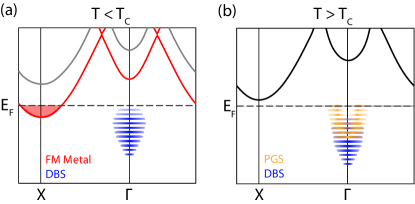
Our findings are summarized in the schematic in Fig. 5. Below , metallic carriers are observed in the spin-polarized conduction band at (0, 2) in addition to minimally dispersive deeply bound states at (0, 0). Upon warming, the exchange splitting of the conduction band is reduced to zero and the metallic carriers and spectral weight at (0, 2) are transferred to (0, 0), where they populate a second dopant-induced state just below , the PGS. These high temperature carriers exhibit a pseudogapped but dispersive lineshape, naturally explaining the increase in resistivity through the metal-insulator transition. Our work reveals for the first time the nature of the FM metal-insulator transition in carrier doped EuO and uncovers an unusual momentum space dependence to the evolution of the electronic structure. We hope that future experimental and theoretical works can resolve the origins of the momentum-space dichotomy and the DBS, since addressing these issues may be key to realizing the potential of EuO-based devices and applications.
We gratefully acknowledge I.S. Elfimov for assistance with DFT calculations; T.Z. Regier (SGM beam line at the Canadian Light Source) for his assistance with the XAS measurements; T. Mairoser, G.A. Sawatzky, and J. Geck for helpful discussions. Research was supported by the National Science Foundation through DMR-0847385 and the MRSEC program under DMR-1120296 (Cornell Center for Materials Research), and by the Research Corporation for Science Advancement (20025). D.E.S. acknowledges support from the National Science Foundation under Grant No. DGE-0707428 and NSF IGERT under Grant No. DGE-0654193. AJM and DGS acknowledge the support of the AFOSR (FA9550-10-1-0123).
References
- (1) Y. Shapira, S. Foner, and T.B. Reed, Phys. Rev. B. 8, 2299 (1973).
- (2) G. Petrich, S. von Molnár, and T. Penney, Phys. Rev. Lett. 26, 885 (1971).
- (3) T. Penny, M.W. Shafer, and J.B. Torrance, Phys. Rev. B. 5 3669 (1972).
- (4) A. Schmehl et al., Nature Mat. 6, 882 (2007).
- (5) P.G. Steeneken et al., Phys. Rev. Lett. 88, 047201 (2002).
- (6) M.W. Shafer and T.R. McGuire, J. Appl. Phys. 39, 588 (1968).
- (7) A.G. Swartz et al., Appl. Phys. Lett. 97, 112509 (2010).
- (8) T.S. Santos and J.S. Moodera, Phys. Rev. B. 69, 241203(R) (2004).
- (9) R. Ulbricht et al., Appl. Phys Lett. 93, 102105 (2008).
- (10) R. Sutarto et al., Phys. Rev. B 80, 085308 (2009).
- (11) See Supplemental Material for discussion of the film characterization, additional photoemission data, and details for the supporting calculations.
- (12) D.E. Eastman, F. Holtzberg, and S. Methfessel, Phys. Rev. Lett. 23, 226 (1969).
- (13) H. Miyazaki et al., Phys. Rev. Lett. 102, 227203 (2009).
- (14) R. Schiller and W. Nolting, Phys. Rev. Lett. 86, 3847 (2001).
- (15) J. Schoenes and P. Wachter, Phys. Rev. B 9, 3097 (1974).
- (16) N.J.C. Ingle and I.S. Elfimov, Phys. Rev. B 77, 121202(R) (2008).
- (17) R. Schiller and W. Nolting, Solid State Commun. 118, 173 (2001).
- (18) E. Bousquet, N.A. Spaldin, and P. Ghosez, Phys. Rev. Lett. 104, 037601 (2010).
- (19) Y. Wang et al., Phys. Rev. B 79, 212408 (2009).
- (20) T. Mairoser et al., Phys. Rev. Lett. 105, 257206 (2010).
- (21) T. Mairoser. Diploma thesis, Universität Augsburg, 2009.
- (22) T. Matsumoto et al., J. Phys.: Condens. Matter 16, 6017 (2004)
- (23) B. Sheu et al., Phys. Rev. Lett. 99, 227205 (2007).
- (24) K.M. Shen et al., Phys. Rev. Lett. 93, 267002 (2004).
- (25) D. Schrupp et al., Europhys. Lett. 70, 789 (2005).
- (26) N. Mannella et al., Nature 438, 474 (2005).
- (27) Y.D. Chuang et al., Science 292, 1509 (2001).
- (28) B.I. Shklovskii and A.L. Efros, Electronic Properties of Doped Semiconductors. (Springer-Verlag, Berlin, 1984).