Homogeneity of Bilayer Graphene
Abstract
We present non-linear transport measurements on suspended, current annealed bilayer graphene devices. Using a multi-terminal geometry we demonstrate that devices tend to be inhomogeneous and host two different electronic phases next to each other. Both of these phases show gap-like features of different magnitude in non-linear transport at low charge carrier densities, as already observed in previous studies. Here, we investigate the magnetic field dependence and find that both features grow with increasing field, the smaller one with 0.6 meV/T, the larger one with a 5-10 times higher field dependence. We attribute the larger of the two gaps to an interaction induced broken symmetry state and the smaller one to localization in the more disordered parts of the device.
keywords:
A. Bilayer graphene; A. Multiterminal device; D. Broken symmetry groundstate; E. Nonlinear transport.1 Introduction
The isolation of monolayer graphene [1] has started a new research field on two-dimensional carbon based electronic systems. Whereas the interest in monolayer graphene mainly stems from its unusual pseudo-relativistic electron dispersion, bilayer graphene promises to be interesting because of its strongly interacting charge carriers. Weak screening in suspended samples and small carrier densities at the charge neutrality point lead to large values for the interaction parameter rS about one order of magnitude larger than in conventional 2DEGs of comparable carrier density [2]. For interaction effects to be observable in electronic transport experiments, bilayer graphene has to be very clean to achieve low charge carrier densities. To reach this regime, the normally used SiO2 substrate has to be removed by underetching, leaving the bilayer freely suspended between the contacts [3, 4]. The suspension allows to current anneal the bilayer graphene flake by Joule heating induced by passing a large current through it. During this heating cycle adsorbates may (at least partially) evaporate.
The exact nature of the electronic groundstate of bilayer graphene has been investigated theoretically for several years [5, 6, 7, 8, 9, 10, 11, 12, 13, 14, 15]. The fourfold degeneracy that stems from the spin and valley degrees of freedom of the charge carriers will be broken by interactions, and new groundstates with partly or totally lifted degeneracies are expected to occur. Interaction induced broken-symmetry states that are being discussed as possible candidates for the groundstate of bilayer graphene include the quantum anomalous Hall insulator (QAH) [11, 12], the quantum spin Hall insulator (QSH) [12], the nematic phase [16, 17], the layer antiferromagnetic phase (LAF) [12, 18, 14], and possibly more. Most, but not all of these states show a gap in the excitation spectrum around =0, leading to a vanishing conductivity around the charge neutrality point (CNP).
We can probe the electronic properties of the graphene bilayer as a function of temperature, charge carrier density and magnetic field by measuring the differential conductance as a function of a bias voltage . We investigate low conducting and insulating samples with similar features as in a previous study, that exhibit two distinct gap-like features in [19], and that mainly differ in the minimum conductance at . Here, we further investigate these kinds of samples by looking at the magnetic field dependence of [20]. Our results suggest that the samples are inhomogeneous after current annealing and are composed of two different electronic phases. A possible reason for this is that the process of current annealing does not clean the samples in a uniform way, but creates almost disorder free areas in the center of the samples and leaves some disorder at the edges, which leads to a coexistence of electronic phases next to each other.
2 Material and methods
Bilayer graphene was deposited onto a p+-doped silicon wafer covered with 300 nm silicon dioxide by micromechanical cleavage of natural graphite. After deposition, a thin (5 nm) film of aluminium was evaporated over the whole wafer. After exposure to air, this film oxidised and transformed to Al2O3 almost completely. Using standard electron-beam lithography, a PMMA etchmask was then structured for shaping the graphene flake using an Ar/O2 plasma, and in a second lithography step, the electrode structures were defined. After each resist development, the exposed part of the oxidised aluminium film was removed in a 25% tetramethylammonium hydroxide (TMAH) solution, thereby eliminating any organic residues left on the graphene. The electrode structures (3 nm Cr and 70 nm Au) were e-gun evaporated, and subsequently the graphene devices were annealed in high vacuum at 10-7 mbar and 200 ∘C for several hours. The silicon dioxide was then partly removed in 2% buffered hydrofluoric acid, leaving the graphene suspended 160 nm above the substrate. The remaining silicon wafer acted as a gate with a voltage applied. The devices were mounted into a 3He cryostat in vacuum and subsequently current annealed at K with typically 0.4 mA per m of flake width [19]. For the present study, we fabricated devices with a four-terminal Hall cross geometry (insets of fig. 1); the longer axis was about 3 m long, the shorter 1.5 m and the width of each individual arm was 1 m. Current annealing was done on pairs of contacts with the other two contacts floating. The annealing process was considered to be successful if a pronounced dip in measured as a function of the gate-voltage appeared in the vicinity of , i.e. at low charge carrier density of at least one contact pair combination.
3 Results
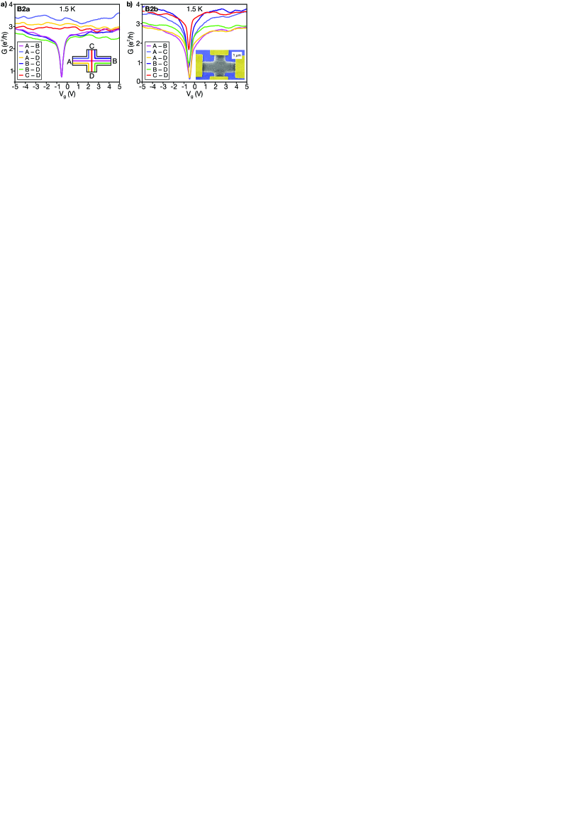
We present data taken on two devices that could successfully be current annealed. Fig. 1 summarises our findings. In the first device, B2a, the current annealing resulted in an inhomogeneous cleaning of the graphene. Fig. 1a) demonstrates that only in two-terminal measurements of that involve contact B a CNP is visible with a minimum conductance of 0.9 e2/h. For all other contact pairs G only fluctuates around 3 e2/h as is changed and does not display a notable minimum. Further annealing rendered the sample more inhomogeneous, leading to gate characteristics with several CNPs at different . In contrast, in B2b the current annealing yielded a more homogeneous device. Fig. 1b) shows as function of for B2b. A CNP at -0.5 V is well developed for all contact pairs. A minimum of 0.2 e2/h at the CNP can be found in measured between contacts A and B. At higher doping, the conductance saturates at 3-4 e2/h.

Performing differential conductance measurements reveals further differences between B2a and B2b. In fig. 2a), a colour scale plot of in B2a as a function of and at 230 mK is shown. The line profile at the CNP at -0.5 V exhibits two gap-like features: a smaller one, called in the following, is present up to 0.6 mV and reduces from 1 e2/h to 0.5 e2/h at zero . The larger feature is visible up to 3.5 mV and lowers from 3 e2/h to about 1 e2/h at zero . Moreover, shows a BCS-like overshoot in . Moving away from the CNP rapidly suppresses . On the other hand, persists as a small zero bias anomaly even in the metallic regime and is visible in the whole accessible gate voltage range. In fig. 2b) the temperature dependence of at the CNP of B2a is plotted. The smaller gap feature, , is totally suppressed if increases from 0.23 K to 1.5 K. The larger feature remains unchanged. The temperature dependence G(T) measured at large carrier density can be fit with a log(T) dependence for T1K.
Device B2b differs from B2a by having a full gap, which reduces to zero at the CNP. Fig. 2c) shows as a function of and at 230 mK. The line profile at the CNP is qualitatively similar to B2a, but is completely suppressed for small . Furthermore, the small gap feature is not readily visible but manifests only as a change in the slope of at 1.5 mV. The larger feature is shifted to higher voltages as well, with 4 mV, and shows a larger overshoot before saturates at 2.3 e2/h. Tuning away from the CNP quenches the larger feature but leaves the smaller intact in agreement to what is observed in B2a. In fig. 2d) the temperature dependence makes better visible. The small gap feature shrinks as is raised from 0.23 K to 1.5 K, but still reduces to zero at 0 mV. A further increase to 4 K completely suppresses . The temperature change from 0.23 K to 1.5 K only reduces the overshoot in the larger feature . Increasing to 4 K yields a reduction of and removes the overshoot.
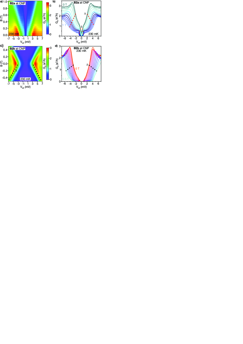
To find out about the origin of the two different features and we perform differential conductance measurements as a function of perpendicular magnetic field, shown in figure 3. Both and increase linearly with but with different slope. Taking the two inflection points of the traces as a measure for and , we can determine to 0.6 meV/T, which is considerably larger than the Zeeman energy of a spin 1/2 (0.12 meV/T for g=2). Looking at the large gap , we find = 2.8 meV/T for sample B2a (Fig. 3b) and 6 meV/T for sample B2b (Fig 3d). As sample B2b showed a full gap already at , the magnetic field dependence of could not be determined here. Similarly, Velasco et al. observed 5.5 meV/T [20] for a fully gapped bilayer graphene device for a gap of similar size as .
The experiments clearly show two distinct gap-like features that occur in different ranges of charge carrier density and temperature, and that show a clearly different magnetic field dependence. We think that this observation can only be explained by the coexistence of different electronic phases next to each other in different parts of the samples. This conjecture is supported by the results of the current annealing procedures shown in figure 1, that can be understood by the existence of almost disorder-free, clean regions that are surrounded by more disordered areas [21, 22], where the current annealing has been less efficient. In the disordered regions the CNP lies outside the charge carrier densities that are accessible to us, due to chemical doping by adsorbates and residues. In this picture, sample B2a would be composed of a clean region close to contact B, and a more disordered rest of the sample. In sample B2b the clean region seems to be larger, occupying the center of the sample, but different CNP conductances between different terminals indicate that even in sample B2b there are regions with stronger disorder that are not evenly distributed, as illustrated in Fig. 4.
We assume that the clean phase is showing an interaction induced gap close to the CNP with vanishing conductivity, and a distinct, BCS like shape. The large increase of with of several meV per tesla has been predicted by theory for certain broken symmetry states like the QAH or QSH [12, 20].
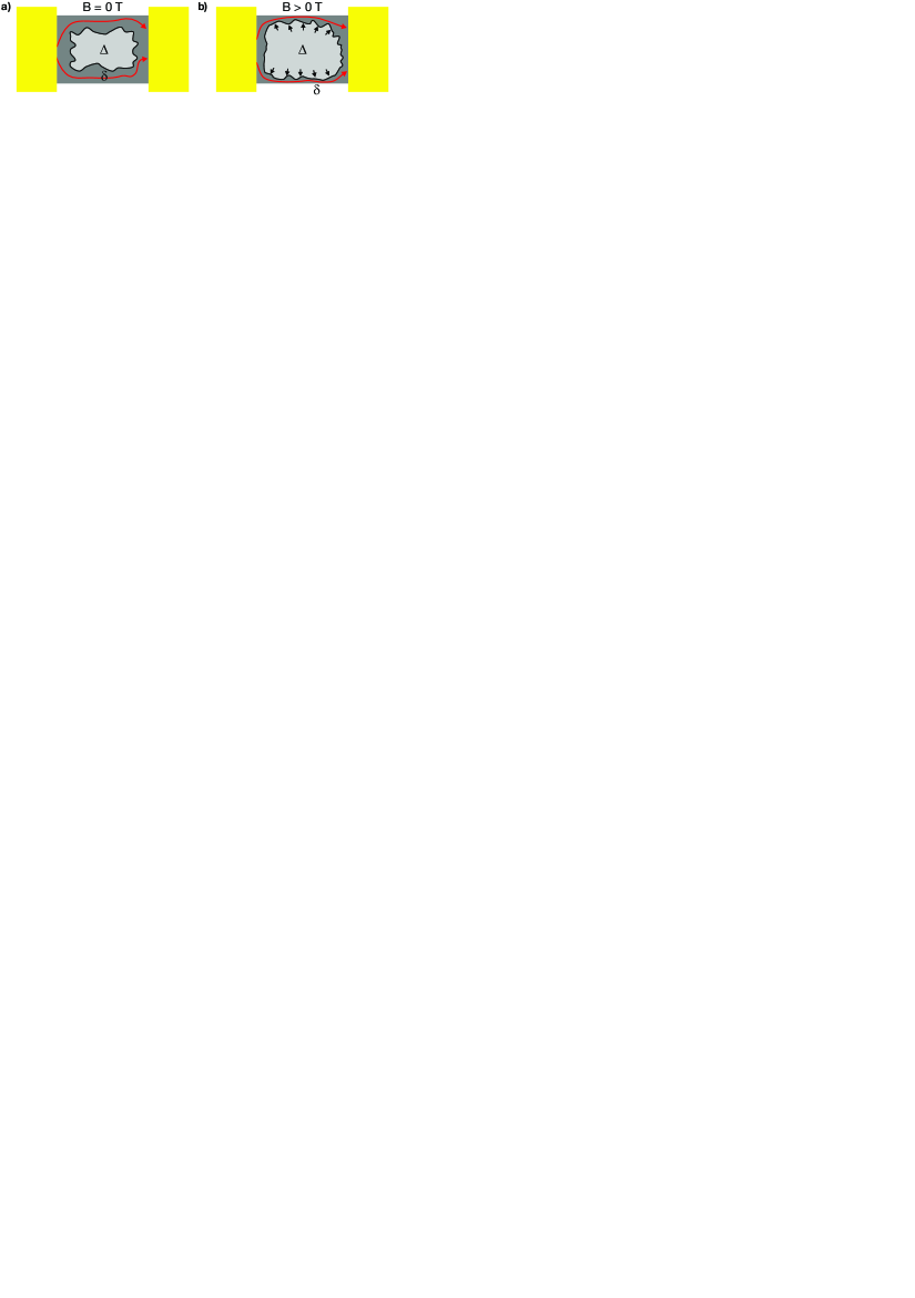
The total conductance of sample B2a is composed of two parallel conduction channels, one through the clean region with gap in the center of the sample, and another, more disordered one along the sample edges with gap-like feature . The origin of the smaller feature is probably disorder induced localization [23, 24, 25]. For a disordered device such as a graphene ribbon with a predetermined geometry the application of a magnetic flux through the sample should lift the localization at least in part. In contrast to this scenario, the small gap in our experiment even increases when a perpendicular magnetic field is applied. We explain this by a change in geometry. The application of a perpendicular magnetic field increases the size of the inner clean region and thereby narrows down the conduction channel at the sample edge (Fig. 4b), leading to increased localization in the disordered part. The different response of the two conduction channels to magnetic field is reflected in the different magnetic field dependence of =0.6 meV/T and =2.8 meV/T.
In sample B2b the initial distribution of the two phases is such that already at B=0 the sample is mostly in the clean phase, and there is only a negligible conductance contribution of the disordered phase at the CNP. This is also the reason for the fact that only a large gap can be observed in , and that is feeble.
Because the metallic contacts will act as a heat sink during current annealing, we also have to assume that the disordered phase persists close to them. In fact, a narrow area of organic deposits can be clearly identified close to the metal contacts in scanning electron micrographs. This disordered region will then decouple the clean area in the sample center from the contacts and thus prevent edge states, that exist in the case of a QAH or QSH phase to couple to the metal contacts. Consequently, any phase in the center of the sample would show insulating behaviour in two terminal conductance, no matter if it has edge-states (QAH, QSH) or not (LAF). As we have shown the current annealing process to be inhomogeneous, we think that is a feature of the disordered graphene regions that persist at the edges of the device. However, as the size of the disordered region will vary from sample to sample, any distribution of versus -gaps may be realized. Different distributions of clean and disordered regions in the samples will lead to different traces around the CNP, with a full suppression of conductance at =0 when the clean region dominates, and some small, finite conductance when there is a considerable region of the disordered phase remaining. The application of a perpendicular magnetic field will always lead to a growth of the gapped -phase at the expense of the conducting -phase, in this way opening a full gap in all samples at some finite value of B. We note that, although not discussed in detail, a small gap was also observed in [20]. It persists at high charge carrier densities and shows a small magnetic field dependence, in contrast to the stronger magnetic field scaling of and in full agreement to our observations.
4 Conclusions
In conclusion, we measured non-linear conductance on multi-terminal, suspended bilayer graphene devices in a Hall-cross geometry as a function of charge carrier density and perpendicular magnetic field. We find that current annealing cleans the graphene inhomogeneously, which leads to samples that are composed of two different regions with distinct electronic properties. Both of these regions show gap-like features at the CNP, as visible in differential conductance . We extract two gaps of different magnitude that show a different temperature dependence and respond differently to magnetic field. Attributing the two gaps to clean and disordered sample regions, we find that the initial distribution of the two regions differs from sample to sample, but that the overall density and magnetic field dependence of the conductance of these two regions is similar. We argue that one of the two regions is a conductive, disordered phase localized at the sample edges that shows a zero bias anomaly over a large range in charge carrier density due to disorder induced localization, and a clean phase in the center of the sample that shows an interaction induced gap close to the charge neutrality point with strongly suppressed conductance. The application of a perpendicular magnetic field favors the expansion of the clean phase in the sample center and shrinks the disordered conducting areas, and therefore pronounces the signature of the interaction effects in differential conductance.
5 Acknowledgments
This work was financed by the Swiss NSF, the ESF programme Eurographene, the EU FP7 project SE2ND, the Swiss NCCR Nano and QSIT. We are grateful to M. Kharitonov and C. N. Lau for discussions.
References
- [1] K. S. Novoselov, A. K. Geim, S. V. Mozorov, D. Jiang, Y. Zhang, S. V. Dubonos, I. V. Grigorieva, A. A. Firsov, Science 306 (2004) 666.
- [2] S. Das Sarma, S. Adam, E. H. Hwang, E. Rossi, Rev. Mod. Phys. 83 (2011) 407.
- [3] K. Bolotin, K. Sikes, Z. Jiang, M. Klima, G. Fudenberg, J. Hone, P. Kim, H. Stormer, Solid State Commun. 146 (2008) 351.
- [4] B. E. Feldman, J. Martin, A. Yacoby, Nature Phys. 5 (2009) 889.
- [5] E. McCann, V. I. Fal’ko, Phys. Rev. Lett. 96 (2006) 086805.
- [6] J. Nilsson, A. H. Castro-Neto, N. M. R. Peres, F. Guinea, Phys. Rev. B 73 (2006) 214418.
- [7] M. Ezawa, Physica E 40 (2007) 269.
- [8] X.-F. Wang, T. Chakraborty, Phys. Rev. B 75 (2007) 041404.
- [9] Y. Barlas, R. Côtè, K. Nomura, A. H. MacDonald, Phys. Rev. Lett. 101 (2008) 097601.
- [10] H. Min, G. Borghi, M. Polini, A. H. MacDonald, Phys. Rev. B 77 (2008) 041407.
- [11] R. Nandkishore, L. Levitov, Phys. Rev. B 82 (2010) 115124.
- [12] F. Zhang, J. Jung, G. A. Fiete, Q. Niu, A. H. MacDonald, Phys. Rev. Lett. 106 (2011) 156801.
- [13] E. Rossi, S. Das Sarma, Phys. Rev. Lett. 107 (2011) 155502.
- [14] M. Kharitonov, arXiv:1109.1553v2.
- [15] Y. Lemonik, I. Aleiner, V. I. Fal’ko, Phys. Rev. B 85 (2012) 245451.
- [16] O. Vafek, K. Yang, Phys. Rev. B 81 (2010) 041401.
- [17] Y. Lemonik, I. L. Aleiner, C. Toke, V. I. Fal’ko, Phys. Rev. B 82 (2010) 201408.
- [18] M. Kharitonov, Phys. Rev. Lett. 109 (2012) 046803.
- [19] F. Freitag, J. Trbovic, M. Weiss, C. Schöneneberger, Phys. Rev. Lett. 108 (2012) 076602.
- [20] J. Velasco, Jr., L. Jing, W. Bao, Y. Lee, P. Kratz, V. Aji, M. Bockrath, C. N. Lau, C. Varma, R. Stillwell, D. Smirnov, F. Zhang, J. Jung, A. H. MacDonald, Nat. Nanotechnol. 7 (2012) 156.
- [21] S. Das Sarma, E. H. Hwang, E. Rossi, Phys. Rev. B 81 (2010) 161407.
- [22] E. H. Hwang, S. Das Sarma, Phys. Rev. B 82 (2010) 081409.
- [23] R. V. Gorbachev, F. V. Tikhonenko, A. S. Mayorov, D. W. Horsell, A. K. Savchenko, Phys. Rev. Lett. 98 (2007) 176805.
- [24] J. B. Oostinga, B. Sacépé, M. F. Craciun, A. F. Morpurgo, Phys. Rev. B 81 (2010) 193408.
- [25] J.-M. Poumirol, A. Cresti, S. Roche, W. Escoffier, M. Goiran, X. Wang, X. Li, H. Dai, B. Raquet, Phys. Rev. B 82 (2010) 041413.