Energy Level Alignment in Organic-Organic Heterojunctions: The TTF-TCNQ Interface
Abstract
The energy level alignment of the two organic materials forming the TTF-TCNQ interface is analyzed by means of a local orbital DFT calculation, including an appropriate correction for the transport energy gaps associated with both materials. These energy gaps are determined by a combination of some experimental data and the results of our calculations for the difference between the TTFHOMO and the TCNQLUMO levels. We find that the interface is metallic, as predicted by recent experiments, due to the overlap (and charge transfer) between the Density of States corresponding to these two levels, indicating that the main mechanism controlling the TTF-TCNQ energy level alignment is the charge transfer between the two materials. We find an induced interface dipole of 0.7 eV in good agreement with the experimental evidence. We have also analyzed the electronic properties of the TTF-TCNQ interface as a function of an external bias voltage between the TCNQ and TTF crystals, finding a transition between metallic and insulator behavior for eV.
Universidad Autónoma de Madrid]Departamento de Física Teórica de la Materia Condensada,
Universidad Autónoma de Madrid, E-28049 Madrid, Spain
Universidad Autónoma de Madrid]Departamento de Física Teórica de la Materia Condensada,
Universidad Autónoma de Madrid, E-28049 Madrid, Spain
Universidad Autónoma de Madrid]Departamento de Física Teórica de la Materia Condensada,
Universidad Autónoma de Madrid, E-28049 Madrid, Spain
Universidad Autónoma de Madrid]Departamento de Física Teórica de la Materia Condensada,
Universidad Autónoma de Madrid, E-28049 Madrid, Spain
1 Introduction
Organic electronics is an area of important research effort where organic materials provide an immense variety of properties and atomic structures. In these materials, interfaces play a key role in fundamental phenomena (e.g. charge separation and charge recombination) for electronic applications such as solar cells and light emitting diodes, to name a few 1, 2, 3.
TTF/TCNQ (tetrathiofulvalene-7,7,8,8,-tetracyanoquinodimethane) is a very interesting organic bulk material that was already studied in the early 70’s showing novel phenomena, like large e- conductivity and superconductivity 4. TTF/TCNQ shows three phase transitions which have been related to condensed charge-density waves, due to Peierls distortions, with transition temperatures of 38, 49 and 54 K 4. Also, the experimental band widths of TTF and TCNQ crystal-bulks are 0.95 and 2.5 eV respectively, while density functional theory (DFT) calculations based on local and semi-local exchange-correlation (XC) functional provide systematically, for TTF and TCNQ, band widths of around 0.65 and 0.70 eV respectively 5, 6, 7, 8. These intriguing properties have prompted a lot of experimental and theoretical studies on the properties of bulk TTF/TCNQ, see e.g. 5, 6, 7, 8, 9, 10; thin films of mixed TTF-TCNQ have also been studied on different substrates like graphene and Au(111) 11, 12.
However, the large amount of work on bulk and thin film properties of TTF/TCNQ contrasts with the much lesser attention dedicated to the interface of the two organic materials. One of the few studies 13 has found that the interface retains its metallic character due to the charge transfer between the two molecules. The existence of an interface dipole layer () 14, 15, generated by charge transfer or/and by polarization effects, and its corresponding vacuum level shift () 1, shows that the Schottky-Mott limit is not satisfied at this interface. Careful spectroscopic characterization of TTF-TCNQ interfaces over different substrates shows a of 0.6 eV and a = HOMOHOMOTCNQ of either 2.1 or 2.4 eV 16, 17.
In this communication we consider the interface between TTF and TCNQ crystals, and analyze the interface energy level alignment and barrier height formation, using a local orbital DFT-approach in which an appropriate correction is included to properly describe the transport gaps of both materials. In section II we present the interface geometries, and in section III we discuss how we determine the transport energy gaps for TTF and TCNQ and give some details about our DFT-calculations. In section IV, we present our results. In particular, our analysis shows that the TTF-TCNQ interface is metallic and that the energy difference between the TCNQLUMO and TTFHOMO is pinned to around 0.8 eV. We have also analyzed how the interface properties depend on the application of an external voltage between the TCNQ and TTF crystals, finding a transition from a metallic to an insulating interface for a voltage of 0.5 eV. Finally, the interfacial geometry has also been analyzed by means of a DFT calculation combined with a semi-empirical parametrization of the van der Waals interaction.
2 Interface Geometry
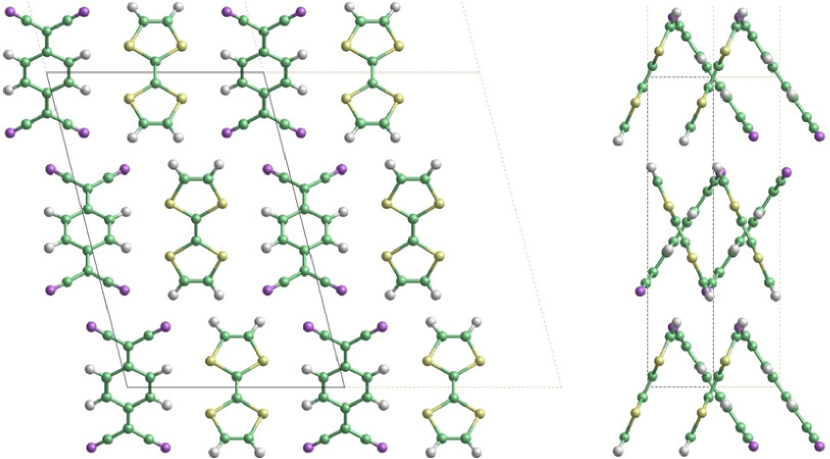
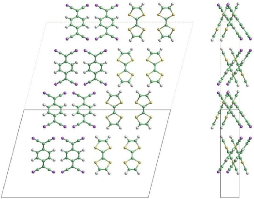
At room temperature, TTF/TCNQ bulk presents a monoclinic structure with lattice parameters a = 12.298 Å, b = 3.819 Å and c = 18.468 Å, and an angle = 104.46° 18 (see 1). However, detailed experimental information of both the geometry and the energetics at the interface is still missing due to inherent difficulties in its structural characterization. For the TTF-TCNQ surface, though, it has been measured by scanning tunneling microscopy 19 and angle-dependent near-edge X-ray adsorption fine structure 20 that the cleaved surfaces are highly ordered and retain the periodicity of the bulk. Thus, in this work we have considered the interfacial structure arising from selecting the interface geometry between TTF and TCNQ layers from the TTF/TCNQ bulk structure along the (100) direction (see 2). In the DFT calculations we have used bulk periodic boundary conditions along b and c vectors, while for the a direction we have considered two cases: a monolayer interface, with only one layer of each material, and a bilayer interface, with 2 TTF and TCNQ layers. This amounts to 2 TTF + 2 TCNQ or 4 TTF + 4 TCNQ molecules in the unit cell, respectively. In the bilayer interface, the second layer is generated from the interfacial plane by adding parallel molecules which are shifted in a similar way as in their independent crystals for both the TTF and TCNQ bulk structures – see Cambridge Structural Database – and satisfying the periodic boundary conditions of keeping b and c vectors from the bulk structure (see 2).
3 TTF-TCNQ Interface Energy Level Alignment
3.1 -SCF calculations
As a first step in order to determine the energy level alignment at the TTF-TCNQ interface, we have performed -SCF calculations for the isolated TTF and TCNQ molecules. In these calculations, the HOMO and LUMO levels are determined from total energy DFT calculations 21, 22 for molecules with , and electrons ( corresponding to the neutral molecule):
| (1) |
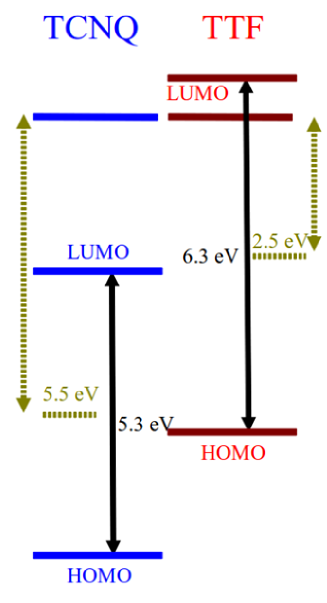
where is the total energy for a molecule with electrons. The results of these calculations are summarized in 3. We obtain a transport gap (difference between and ) of 5.3 eV and 6.3 eV for TCNQ and TTF, respectively, while the mid-gap positions are found to be located at 5.5 eV (TCNQ) or 2.5 eV (TTF) below the Vacuum Level ().
3.2 Energy levels at the interface
The energy level values for the isolated molecules have to be corrected due to the interaction with the other molecules in the crystal and at the interface. The effect of this ‘environment’ is three-fold: (a) broadening of the energy levels into bands; (b) relative shift of the TTF and TCNQ molecular levels due to electrostatic and Pauli exclusion effects; (c) Polarization or screening effects, shifting in different directions occupied and empty states. Point (b) gives rise to a Vacuum Level Shift (), or interface potential, between both crystals, while the effect of point (c) is a reduction of the transport gaps at the interface (or in the crystals) as compared with the values for isolated TTF or TCNQ molecules, . For example, for a molecule interacting with a metal, image potential effects reduce the transport gap as follows: , where is the image potential 23. In the case of an organic crystal (or interface) a similar effect is present, due to the screening/polarization of the other molecules.
In order to obtain the energy level alignment for the TTF-TCNQ interface, we have used a combination of experimental and theoretical information:
- (1)
-
(2)
The mid-gap energies obtained in the -SCF calculations mentioned above are 5.5 eV (TCNQ) and 2.5 eV (TTF) below their corresponding Vacuum Level () positions.
-
(3)
As discussed below, we find that 0.8 eV, a result that is related to the experimental observation that the interface is metallic 14, see below.
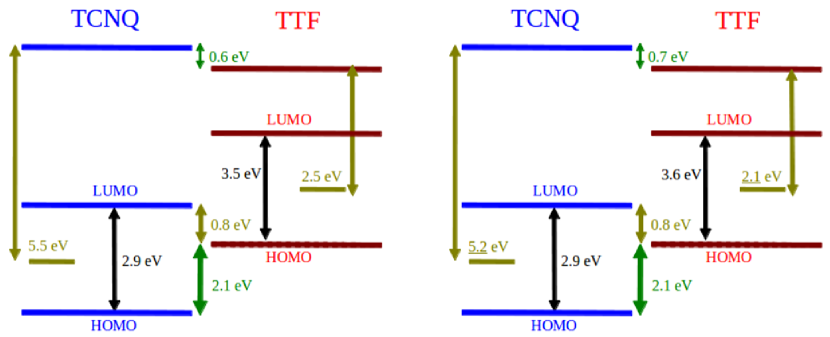
Using this information, we can deduce that at the interface the transport gap is 2.9 eV for TCNQ, and 3.5 eV for TTF, i.e. screening/polarization effects reduce the transport gaps by 2.4 eV (TCNQ) and 2.8 eV (TTF). 4 (left panel) summarizes the resulting energy level alignment for the TCNQ-TTF interface.
3.3 DFT calculations
We have performed DFT calculations for the monolayer and bilayer periodic interface structures presented in section II (see 2). In these calculations we have used a local-orbital DFT code 24, and the initial transport gaps for TCNQ and TTF have been adjusted to the values given in 4 (left panel) using a scissor operator; besides, the initial TTF and TCNQ molecular levels are shifted in such a way that their initial positions have the same value, and the initial mid-gap positions correspond to the values given in 4 (left panel) (see e.g. Refs. 25, 26, 27 and references therein for details). Other technical details are the use of the local density approximation (LDA) and an optimized basis set of (H) and (C, N and S) Numerical Atomic-like Orbitals 28, with the following cut-off radii (in a.u.): =4.1 for H, and =4.0, 3.6, 4.2, =4.5, 4.1, 4.7, and =5.4, 5.2, 5.5 for C, N and S, respectively.
4 Results and Discussion
The right panel of 4 shows the TCNQ-TTF interface energy level diagram obtained in our DFT calculations (explained in third subsection of previous section) with the initial conditions as explained above. This self-consistent result is quite similar to the energy level diagram obtained in second subsection of previous section, shown in the left panel of 4. The band-gaps and interface dipole are quite similar in both panels of 4, however the mid-gap positions move slightly upwards by around 0.3-0.4 eV. This shift is due to the Pauli repulsion (related to the Pauli exclusion principle).
In order to analyze the mechanism responsible for the energy level alignment at the TTF-TCNQ interface, we have performed DFT calculations as described in third subsection of previous section, in which we shift by the initial (before self-consistency) position of the molecular levels of TCNQ with respect to the molecular levels of TTF; = 0 corresponds to equal initial vacuum level positions, and 0 corresponds to a destabilization of the TCNQ levels, w.r.t. the TTF levels. This shift simulates the application of a bias potential of value between the two crystals. 4 (right panel) represents the final levels (after self-consistency) for the = 0 case. A change in the initial relative position of the TCNQ and TTF energy levels will influence the induced dipole and the rest of the electronic properties at the interface. The final will depend on the initial misalignment setup (e.g. the external bias between the two crystals) and on the induced potential after electronic self-consistency, , in such a way:
| (2) |
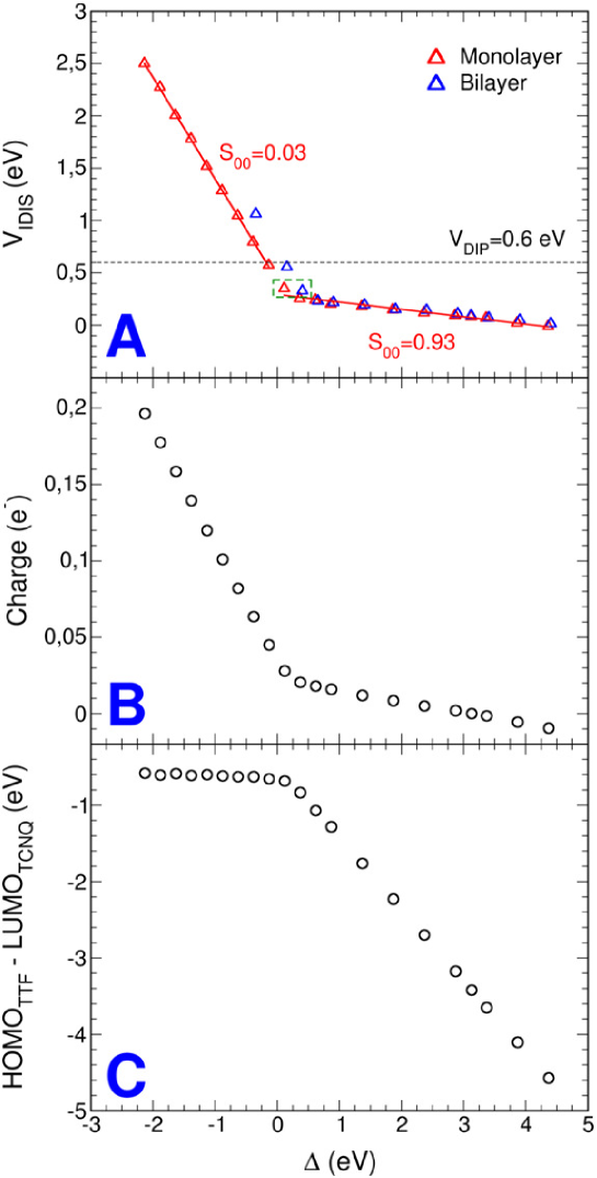
In 5A we depict as a function of for the mono and bilayer-interfaces. In both graphs two different regimes are clearly observed, split by a crossing point located at = 0.2 (0.45) eV for the monolayer (bilayer) case. For both regimes, we see that:
| (3) |
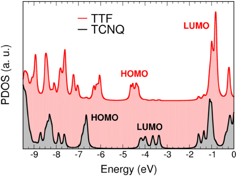
being a screening parameter 23, taking the value 0.03 for 0.2 (0.45) eV and 0.93 for 0.2 (0.45) eV. The case of 0.2(0.45) eV corresponds to a metallic phase in which the and Densities of States (DOS) are overlapping, as shown in 6 and 7; in this case, the difference between and is almost constant ( 0.8 eV), due to the transfer of charge between these two levels. For the other phase, 0.2(0.45) eV, we find a typical heterojunction with small screening and a small induced potential, .
This is illustrated in 5B-C, where we depict, for the monolayer interface, the charge transfer (positive if electron charge flows from TTF to TCNQ) and the value of vs. . For both plots the crossing point between the two different regimes is located at the same position than for , close to 0.2 eV, dividing the charge transfer plot into a regime with a large increase of charge transfer as is reduced, for 0.2 eV, and another in which the transfer of charge is small and changes rather slowly as is increased, for 0.2 eV. In 5C we see that for 0.2 eV the value of vs. presents a slope close to -1, while for 0.2 eV is approximately constant, with a value of -(0.7-0.8) eV. This value ( 0.8 eV) has been used in second subsection of previous section (see left panel of 4) to deduce the TCNQ and TTF energy level positions at the interface. It is worth mentioning that zero charge transfer corresponds to the case of 3.12 eV; for this alignment is not, however, zero, but takes the values 0.10 and 0.11 eV for the mono and the bilayer cases, respectively. These induced potentials are created by the polarization effects of the molecule.
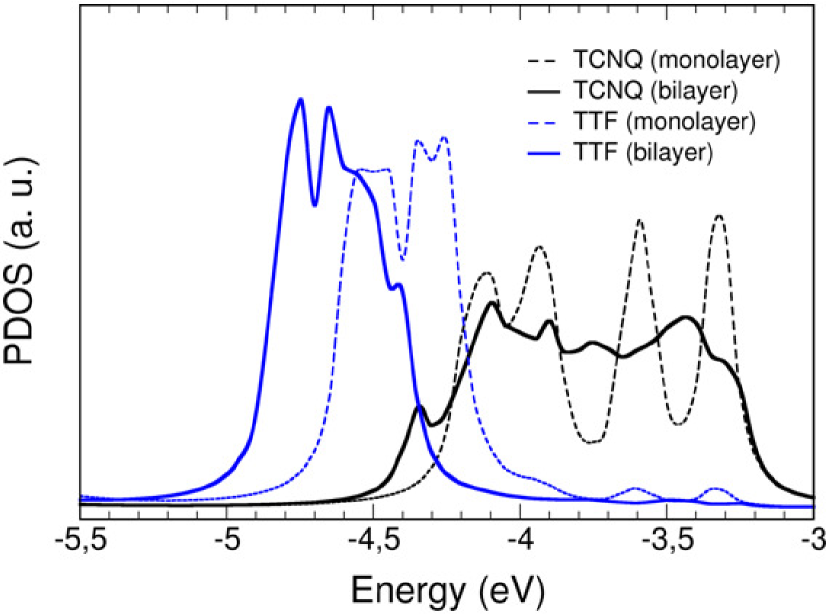
In 5 we observe that from the monolayer to the bilayer case the crossing point moves around 0.25 eV to positive values of . This is explained in 7, that shows, for the monolayer and bilayer interfaces, the DOS projected on each material for a value of close to the crossing point. We notice that there is a broadening for the bilayer case of the DOS, which shifts by 0.25 eV the position where this DOS starts to overlap with the DOS corresponding to the , as compared with the monolayer case.
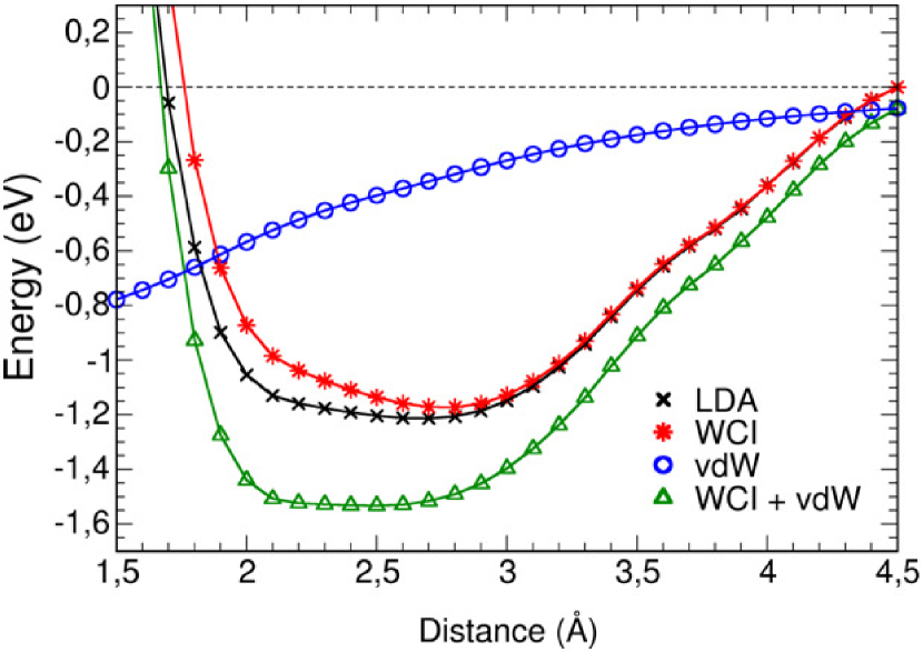
Finally, as a check of the interface geometry used (see 2), we have calculated the total energy as a function of the distance between the TTF and TCNQ layers at the interface. 8 shows the total energy curves for the LDA calculation and the van der Waals (vdW) interactions energy; this energy is included in a semiempirical fashion as an atractive atom-atom term. is the Grimme damping expresion 29 and =0.7, where is the interatomic parameter calculated using the London dispersion relation as a function of the atomic polarizability and the first ionization potential 30; 0.7 is a constant correction calculated from a detailed analysis of the C–C interaction 31, which is applied to every parameter. In order to prevent for the over-counting that would appear including both, the exchange-correlation energy provided by a conventional LDA and the correlation energy associated with the long-range vdW interaction, we have also performed a “corrected LDA” calculation in which the exchange-correlation energy for the complete system is calculated as the sum of the exchange-correlation energies for each subsystem, taken each one independently, neglecting in this way the effect of the overlapping densities in the exchange-correlation energy 32. In 8 this interaction energy is labeled weak chemical interaction (WCI). The minimum of the WCI+vdW total energy curve is around 2.5 Å, which is close to the experimental value for the distance between TTF and TCNQ layers in bulk TTF/TCNQ; notice, however, the very flat energy profile (within 0.02 eV) from 2.2 to 2.7 Å. This result suggests that starting from the bulk structure to generate the interface geometry is a good approximation.
5 Conclusions
In conclusion, we have presented a DFT analysis of the energy level alignment in the TTF/TCNQ interface, introducing in a self-consistent fashion appropriate transport gaps for both materials as determined from a combination of experimental and theoretical information. In these calculations we have also analyzed the metal-insulator phase-transition occurring in this interface when applying a bias voltage between the two materials. We find that at zero bias the interface is metallic while for bias larger than 0.5 eV (shifting TTF towards higher binding energies w.r.t. TCNQ) the system becomes an insulator. Our results have been favorably compared with the experimental data, indicating that the main mechanism controlling energy level alignment in the TTF/TCNQ interface is the charge transfer between both organic semiconductors.
6 Acknowledgements
This work is supported by Spanish MICIIN under contract FIS2010-16046, the CAM under contract S2009/MAT-1467 and the European Project MINOTOR (Grant FP7-NMP-228424). JIB gratefully acknowledges financial support by the European Project MINOTOR. JIM acknowledges funding from Spanish MICIIN through Juan de la Cierva Program. Special thanks to Dr. Daniel González for the development of the Xeo software package, which has been extensively used for the data analysis.
References
- 1 H. Ishii, K. Sugiyama, E. Ito, and K. Seki, Adv. Mat. 11, 605 (1999).
- 2 N. R. Armstrong, W. Wang, D. M. Alloway, D. Placencia, E. Ratcliff, and M. Brumbach, Macro. Rapid Comm. 30, 717 (2009).
- 3 N. Koch, ChemPhysChem 8, 1438 (2007).
- 4 D. Jérome, and H. J. Schulz, Adv. Phys. 31, 299 (1982).
- 5 F. Zwick, D. Jérome, G. Margaritondo, M. Onellion, J. Voit, and M. Grioni, Phys. Rev. Lett. 81, 2974 (1998).
- 6 M. Sing, U. Schwingenschlögl, R. Claessen, P. Blaha, J. Carmelo, L. Martelo, P. Sacramento, M. Dressel, and C. Jacobsen, Phys. Rev. B 68, 125111 (2003).
- 7 L. Cano-Cortés, A. Dolfen, J. Merino, J. Behler, B. Delley, K. Reuter, and E. Koch, Eur. Phys. J. B 56, 173 (2007).
- 8 J. Fraxedas, Y. Lee, I. Jiménez, R. Gago, R. Nieminen, P. Ordejón, and E. Canadell, Phys. Rev. B 68, 195115 (2003).
- 9 A. J. Heeger J. P. Pouget, S. K. Khanna, F. Denoyer, R. Comes, and A. F. Garito, Phys. Rev. Lett. 37, 437 (1976).
- 10 S. Ishibashi, Sci. Tech. Adv. Mat. 10, 024311 (2009).
- 11 J. T. Sun, Y. H. Lu, W. Chen, Y. P. Feng, and A. T. S. Wee, Phys. Rev. B 81, 155403 (2010).
- 12 N. González-Lakunza, I. Fernández-Torrente, K. Franke, N. Lorente, A. Arnau, and J. Pascual, Phys. Rev. Lett. 100, 156805 (2008).
- 13 H. Alves, A. S. Molinari, H. Xie, and A. F. Morpurgo, Nat. Mat. 7, 574 (2008).
- 14 D. Beljonne, J. Cornil, L. Muccioli, C. Zannoni, J. Brédas, and F. Castet, Chem. Mat. 23, 591 (2011).
- 15 I. Avilov, V. Geskin, and J. Cornil, Adv. Func. Mat. 19, 624 (2009).
- 16 S. Braun, X. Liu, W. R. Salaneck, and M. Fahlman, Org. Elect. 11, 212 (2010).
- 17 R. J. Murdey, and W. R. Salaneck, Jap. J. App. Phys. 44, 3751 (2005).
- 18 T. J. Kistenmacher, T. E. Phillips, and D. O. Cowan, Acta Crys. B 30, 763 (1974).
- 19 T. Sleator, and R. Tycko, Phys. Rev. Lett. 60, 1418 (1988).
- 20 M. Sing, J. Meyer, M. Hoinkis, S. Glawion, P. Blaha, G. Gavrila, C. Jacobsen, and R. Claessen, Phys. Rev. B 76, 245119 (2007).
- 21 M. A. L. Marques et al., Comput. Phys. Commun. 151, 60 (2003).
- 22 C. Adamo, G. E. Scuseria, and V. Barone, J. Chem. Phys. 111, 2889 (1999).
- 23 F. Flores, J. Ortega, and H. Vázquez, Phys. Chem. Chem. Phys. 11, 8658 (2009).
- 24 J. P. Lewis, P. Jelínek, J. Ortega, A. A. Demkov, D. G. Trabada, B. Haycock, H. Wang, G. Adams, J. K. Tomfohr, E. Abad, H. Wang, and D. A. Drabold, Phys. Stat. Sol. B 248, 1989 (2011).
- 25 B. Pieczyrak, E. Abad, F. Flores, and J. Ortega, J. Chem. Phys. 135, 084702 (2011).
- 26 J. I. Martínez et al., Phys. Stat. Sol. B 248, 2044 (2011).
- 27 J. I. Martínez et al., Org. Elec. 13, 399 (2012).
- 28 M. A. Basanta et al., Comput. Mat. Sci. 39, 759 (2007).
- 29 S. Grimme, J. Comput. Chem. 27, 1787 (2006).
- 30 “CRC Handbook of Chemistry and Physics”, Ed. D. R. Lide, 79th ed., CRC Press (1998).
- 31 Y. J. Dappe, J. Ortega, and F. Flores, Phys. Rev. B 79, 165409 (2009).
- 32 E. Abad, J. Ortega, and F. Flores, Phys. Stat. Sol. A 209, 636 (2012).