Frequency and Q-factor control of nanomechanical resonators
Abstract
We present an integrated scheme for dielectric drive and read-out of high-Q nanomechanical resonators which enables tuning of both the resonance frequency and quality factor with an applied DC voltage. A simple model for altering these quantities is derived, incorporating the resonator’s complex electric polarizability and position in an inhomogeneous electric field, which agrees very well with the experimental findings as well as FEM simulations. By comparing two sample geometries we are able to show that careful electrode design can determine the direction of frequency tuning of flexural in- and out-of-plane modes of a string resonator. Furthermore we demonstrate that the mechanical quality factor can be voltage reduced more than fivefold.
Control of small-scale mechanical systems is essential for their application. Resonant micro- and nanoelectromechanical systems (M/NEMS) have both proven themselves technologically viable (frequency filtering in cell phones Bouchaud and Wicht (2005), gyroscopes Dean and Luque (2009), atomic force microscope (AFM) cantileversBinnig et al. (1986)) as well as shown great promise for next-generation sensor applications (mass sensors Naik et al. (2009); Li et al. (2010); Chaste et al. (2012), resonant bio sensors Burg et al. (2007) and ultra sensitive force sensors Mamin and Rugar (2001); Regal et al. (2008)). Three areas of development are central to realizing the potential of high performance resonant micro- and nanomechanics: advancement of high Q geometries and materials; improved readout schemes for mechanical motion, including compactness and integrability; and increased control of the resonant behavior of the mechanics. In the field of nanomechanics, the last years have seen the advent of high Q silicon nitride strings under high tensile stress Verbridge et al. (2006), as well as indications that the stress rather than the nitride is responsible for the high mechanical quality factor Unterreithmeier et al. (2010). Subsequently, efficient integrated drive and read-out schemes have been developed to detect the sub-nanoscale motion of small-scale resonant mechanicsEkinci (2005). Very good tunability of the resonance frequency can be achieved by capacitive coupling of the nanomechanical element to a side electrode Kozinsky et al. (2006). However, the required metalization of the resonant structure reduces the room temperature quality factor significantlyYu et al. (2012) via Ohmic losses. In our lab, an efficient, room-temperature microwave mixing scheme has been developed for readout Faust et al. (2012a), as well as a dielectric drive mechanism to actuate mechanics regardless of their material make-upUnterreithmeier et al. (2009), importantly obviating the necessity to metallize otherwise low-loss dielectrics. In this paper we present a continuation of this development that enables tuning of both the frequency and quality factor of nanomechanical resonators in the context of this highly applicable and integrable scheme. Using the combined dielectric actuation and microwave readout schemes, we theoretically develop the means to controllably raise and lower the resonant frequency of various flexural modes of our mechanics, as well as to broaden the mechanical resonance linewidth. The latter so-called Q control Rodriguez and Garcia (2003); Sulchek et al. (2000)is widely used in AFM measurements and grants faster image acquisition rates by decreasing the mechanical response time. In the presented scheme this Q control is achieved by simply applying a DC voltage instead of the normally employed active feedback mechanism and is thus well suited for integration. The theoretical relationship between the design of the electrodes and the resulting control of a given mode is validated both by experiment and simulation.
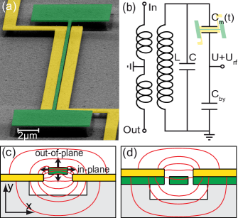
Our system is depicted in Fig. 1(). A nanomechanical silicon nitride string is situated between a pair of near-lying electrodes (Fig. 1(a)). A DC voltage across the electrodes produces an electric field that induces a dipolar moment in the silicon nitride string, which thus experiences a force in the gradient field. This force can be modulated by an additional AC voltage, actuating the mechanical resonanceUnterreithmeier et al. (2009). Additionally, the mechanical resonator is dielectrically coupled to an external microwave cavity via the same electrodes. An equivalent circuit diagram is shown in Fig. 1(b). Deflection of the beam translates into a change of the capacitance between the two electrodes and thereby modulates the cavity transmission signal.
The mechanical oscillation can then be detected by demodulating this signal. A more detailed description of this room temperature heterodyne detection including the demonstration of self-oscillation caused by cavity backaction can be found elsewhere Faust et al. (2012a).
To enable direct actuation of the mechanical resonator, we introduce a microwave bypass between ground and one of the electrodes using the single layer capacitor (SLC)111500U04A182KT4S from Johanson Technology . Thus a DC and RF voltage can be applied to this electrode, whereas the other electrode is grounded via the microstrip cavity (compare Fig. 1(b)). Consequently, the presented integrated configuration combines the above mentioned cavity-enhanced detectionFaust et al. (2012a) with dielectric driving and tuning Unterreithmeier et al. (2009). Note that the drive and detection can be realized with a single set of electrodes, since crosstalk is avoided by operating the cavity at 3.5 GHz, well-separated in frequency from the mechanical fundamental flexural mode frequency of here 6.5 MHz.
For this study, two sample geometries for obtaining optimized gradient field coupling are fabricated from high-stress silicon nitride using standard electron beam lithography, reactive ion etching and subsequent hydrofluoric wet etching to obtain suspended strings. To minimize Ohmic losses of the microwave circuit originating in the bulk chip supporting the mechanical resonator, we use a fused silica substrate instead of silicon. The geometries are schematically shown in Fig. 1(c,d). Referring to the beam’s position with respect to the electrodes, the two structures will from now on be referenced as “elevated” (Fig. 1(c)) and “lowered” (Fig. 1(d)). The centerpiece of each structure is the 55 µm long silicon nitride string resonator with a rectangular cross section of width 260 nm and height 100 nm. The freely suspended resonator is bordered by two vertically offset gold electrodes, one of which is connected to the microstrip cavity with a resonance frequency of 3.5 GHz and a quality factor of 70, while the other electrode leads to the SLC. The essential difference between the geometries is the vertical positioning of the beam with respect to the gold electrodes. This affects the dielectric environment and thereby the electric field lines as depicted in Fig. 1(c,d). In the elevated design shown in Fig. 1(c), the upper edge of the electrodes coincides with the lower edge of the beam, whereas in the lowered design in Fig. 1(d), the upper edge of the beam coincides with the lower edge of the electrodes. The simulated electric field lines for both geometries are obtained from finite element simulations using COMSOL Multiphysics and allow us to extract the electric field along the x- and y-direction. These inhomogeneous electric fields cause force gradients for the in- and out-of-plane modes of the resonator. They thus alter the restoring force of the respective mode and thereby its resonance frequency Unterreithmeier et al. (2009). At the same time, the mechanical quality factor can be altered with the DC voltage, as the strong electric field and high field gradient lead to velocity-dependent dielectric losses in the beam material. This frequency and linewidth tuning can be described by a simple model which agrees very well with our experimental findings and finite element simulations. The resonance frequency can be tuned over 5 % and the resonance linewidth can be increased by a factor of 6.
We find the force gradient to be proportional to the square of the voltage and thus expect a quadratic dependence of the resonator resonance frequency on the applied DC voltage. This can be derived from the energy of the induced dipolar moment of the dielectric resonator in an external electric field , where is the polarizability of the silicon nitride beam. Assuming that and are parallel, i. e. using a scalar, complex polarizability and introducing a dependence of the electric field on the variable coordinate , the energy reads
| (1) |
Here can be the x- or y-coordinate (compare Fig. 1(c)), so the following considerations apply to both the in- and out-of-plane mode. Assuming for small displacements, the total energy can be separated into a real (stored) and an imaginary (dissipative) part.
| (2) | |||
| (3) |
The stored energy is related to the frequency shift of the mechanical resonator, as the second derivative of this energy provides an additional force gradient i. e. an electrically induced spring constant :
| (4) |
Hence the shift in resonance frequency caused by the electrical spring constant can be expressed in experimentally accessible units as
| (5) |
which assumes both, the electrical frequency shift to be much smaller than the mechanical frequency and a geometry-dependent proportionality between the applied voltage and the resulting electric field gradient . Moreover, as predicted by our finite-element simulations the sign of the gradient (corresponding to the sign of ) depends on the chosen geometry such that the out-of-plane mode changes its tuning direction between the elevated and the lowered design, which does not occur for the in-plane modes.
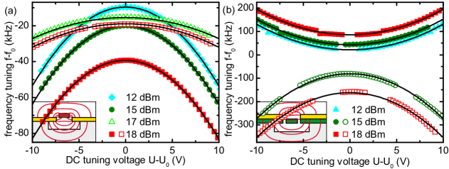
The quadratic tuning behavior with DC voltage is found to agree very well with the experimental data, as displayed in Fig. 2(). All measurements are conducted at room temperature and a pressure of mbar. For each mode and geometry the mechanical spectrum of both modes is taken for different DC voltages and microwave powers. The driving voltage is kept constant in every measurement. The values for lie within 80 µV and 1 mV depending on the particular mode and geometry.
A Lorentzian fit to each mechanical spectrum yields the resonance frequency and the quality factor of the resonance for each parameter set. The resonance frequencies lie around 6.5 MHz and the highest quality factor is for the out-of-plane mode in the elevated design. Note that the tuning with microwave power is a result of the effective microwave voltage Faust et al. (2012a), and so is analogous to the tuning with a DC voltage. Subsequently, we fit to the tuning curves shown in Fig. 2(), using the natural resonance frequency and two tuning parameters for the DC voltage and the effective microwave voltage , as the DC and high frequency polarizability might differ. We also introduce the DC offset to account for a shift (typically less than 1 V) of the vertex of the tuning parabola away from zero DC voltage, which is most likely caused by trapped charges in the dielectric resonator material. As the influence of the microwave field on static dipoles averages out, there is no such shift resulting from the microwave voltage . Consequently, we can extract the tuning parameters for each geometry and oscillation direction. With increasing voltage and for the elevated geometry depicted in Fig. 2(a), both the in- and out-of-plane mode tune to lower frequencies, whereas for the lowered design (Fig. 2(b)), the out-of-plane mode tunes to higher frequencies, as predicted by our simulations. The solid black lines in Fig. 2() show the fit of our model with a single set of parameters for each mode in excellent agreement with the data. In the case of opposite frequency tuning, the initial frequency difference of the in- and out-of-plane modes can be evened-out, which leads to an avoided crossing caused by a coupling between the modes Faust et al. (2012b). As the data points in this coupling region deviate from normal tuning behavior, they have been omitted in Fig. 2(b).
Altering the DC or effective microwave voltage does not only shift the resonance frequency, but also influences the damping of the mechanical resonance and thereby the measured linewidth . Like the resonance frequency, the damping varies quadratically with increasing voltage. This can be understood by analyzing the dissipated energy given by equation (3): A time average of this quantity over one period of mechanical vibration gives
| (6) | |||||
Here we omit the term (as , otherwise static electric fields would lead to dissipation). As the mechanical stored energy is much larger than the electrical energy , one can approximate the additional electrical damping to be
| (7) |

The measured damping versus DC voltage is shown in Fig. 3(). It displays the quadratic behavior of the damping constant of the out-of-plane mode in the elevated design for two different microwave powers. Here is the intrinsic damping of the resonator and is given by equation (7). Again, the vertical offset between the two curves is explained by the effective microwave voltage acting analogously to a DC voltage. The solid lines in Fig. 3() are a fit of the model to the data, from which the curvature can be extracted.
Using this curvature and equation (7), the imaginary part of the polarizability can be expressed by
| (8) |
Similarly, employing the curvature of the parabolic frequency shift and using equation (5) an expression for the real part can be given:
| (9) |
The ratio
| (10) |
is then independent of all resonator parameters and can be determined from the two curvatures.
The measured values for damping and tuning curvatures are and , leading to . By using the Clausius-Mossotti-Relation to first calculate the (lossless) using , one can determine the dielectric loss tangent
| (11) |
This value is well within the range of loss tangents reported for silicon nitride thin films Gould (2003). Note that the time-varying capacitance induces a dissipative current in the electrodes, which also leads to a quadratically increasing dampingKozinsky et al. (2006). However, using values obtained from FEM simulations for the electrode capacitance and its variation with beam deflectionUnterreithmeier et al. (2009), we estimate that this damping is three orders of magnitude smaller than that caused by dielectric losses. The relevant effect for the additional damping with increasing DC voltage is thus the dissipative reorientation of the dipoles in the resonator caused by its motion in a static, inhomogenous electric field, as described by equation (6).
The DC voltage dependence of the mechanical damping was also measured at zero microwave power using an optical detection technique Kouh et al. (2005). The resulting was within a few percent of the value extracted from the 9 dBm curve in Fig. 3(), demonstrating that a measurement at low microwave powers induces only negligible additional damping to the mechanical resonator.
In conclusion, we show dielectric frequency tuning of over 5 % of the natural resonance frequency for nanomechanical resonators in an all-integrated setup that requires no metallization of the resonant mechanical structure itself. This scheme thus maintains an excellent quality factor of up to at and . Furthermore, by careful design of the geometry, one can choose the tuning behavior of the out-of-plane mode to be either upward or downward in frequency and thus tune the two orthogonal resonator modes both in the same and in opposite directions. We demonstrate that dielectric losses become highly relevant when using nanoscale electrode geometries generating large field gradients providing high tunability. This could be used as a Q control Rodriguez and Garcia (2003); Sulchek et al. (2000); Venstra et al. (2011) that does not require any active electronics such as a phase-locked loop but rather a single DC voltage. Such a Q control can be employed to increase the bandwidth of NEMS sensors significantly, leading to much more adaptable devices. Without the need for active electronics this could prove to be very well suited for integrated designs. Together with microwave cavity backaction Faust et al. (2012a) the mechanical resonance linewidth can be controlled from a few Hz up to more than 100 Hz, thereby tuning the mechanical bandwidth by about two orders of magnitude. Finally, we imagine that the scheme presented can also be employed to build self-sensing AFM cantileversLi et al. (2007) with tunable bandwidth and resonance frequency that are not subject to the bandwidth limitations of the normally employed piezo drive and could thus be used in multifrequency force microscopy schemes Garcia and Herruzo (2012).
Acknowledgements.
Financial support by the Deutsche Forschungsgemeinschaft via Project No. Ko 416/18, the German Excellence Initiative via the Nanosystems Initiative Munich (NIM) and LMUexcellent, as well as the European Commission under the FET-Open project QNEMS (233992) is gratefully acknowledged. We thank Darren R. Southworth for critically reading the manuscript.References
- Bouchaud and Wicht (2005) J. Bouchaud and H. Wicht, in Society of Photo-Optical Instrumentation Engineers (SPIE) Conference Series, Society of Photo-Optical Instrumentation Engineers (SPIE) Conference Series, Vol. 5717, edited by A. K. Henning (2005) pp. 50–54.
- Dean and Luque (2009) R. Dean and A. Luque, Industrial Electronics, IEEE Transactions on 56, 913 (2009).
- Binnig et al. (1986) G. Binnig, C. F. Quate, and C. Gerber, Phys. Rev. Lett. 56, 930 (1986).
- Naik et al. (2009) A. K. Naik, M. S. Hanay, W. K. Hiebert, X. L. Feng, and M. L. Roukes, Nature Nanotechnology 4, 445 (2009).
- Li et al. (2010) M. Li, E. B. Myers, H. X. Tang, S. J. Aldridge, H. C. McCaig, J. J. Whiting, R. J. Simonson, N. S. Lewis, and M. L. Roukes, Nano Letters 10, 3899 (2010).
- Chaste et al. (2012) J. Chaste, A. Eichler, J. Moser, G. Ceballos, R. Rurali, and A. Bachtold, Nat Nano 7, 301 (2012).
- Burg et al. (2007) T. P. Burg, M. Godin, S. M. Knudsen, W. Shen, G. Carlson, J. S. Foster, K. Babcock, and S. R. Manalis, Nature 446, 1066 (2007).
- Mamin and Rugar (2001) H. J. Mamin and D. Rugar, Applied Physics Letters 79, 3358 (2001).
- Regal et al. (2008) C. A. Regal, J. D. Teufel, and K. W. Lehnert, Nat Phys 4, 555 (2008).
- Verbridge et al. (2006) S. S. Verbridge, J. M. Parpia, R. B. Reichenbach, L. M. Bellan, and H. G. Craighead, Journal of Applied Physics 99, 124304 (2006).
- Unterreithmeier et al. (2010) Q. P. Unterreithmeier, T. Faust, and J. P. Kotthaus, Physical Review Letters 105, 027205 (2010).
- Ekinci (2005) K. Ekinci, Small 1, 786 (2005).
- Kozinsky et al. (2006) I. Kozinsky, H. W. C. Postma, I. Bargatin, and M. L. Roukes, Applied Physics Letters 88, 253101 (2006).
- Yu et al. (2012) P.-L. Yu, T. P. Purdy, and C. A. Regal, Physical Review Letters 108, 083603 (2012).
- Faust et al. (2012a) T. Faust, P. Krenn, S. Manus, J. P. Kotthaus, and E. M. Weig, Nat Commun 3, 728 (2012a).
- Unterreithmeier et al. (2009) Q. P. Unterreithmeier, E. M. Weig, and J. P. Kotthaus, Nature 458, 1001 (2009).
- Rodriguez and Garcia (2003) T. R. Rodriguez and R. Garcia, Appl. Phys. Lett. 82, 4821 (2003).
- Sulchek et al. (2000) T. Sulchek, R. Hsieh, J. D. Adams, G. G. Yaralioglu, S. C. Minne, C. F. Quate, J. P. Cleveland, A. Atalar, and D. M. Adderton, Applied Physics Letters 76, 1473 (2000).
- Note (1) 500U04A182KT4S from Johanson Technology.
- Faust et al. (2012b) T. Faust, J. Rieger, M. J. Seitner, P. Krenn, J. P. Kotthaus, and E. M. Weig, Phys. Rev. Lett. in press arXiv:1201.4083v2 (2012b), arXiv:1201.4083 [cond-mat.mes-hall] .
- Gould (2003) R. Gould, Thin Solid Films 433, 309 (2003).
- Kouh et al. (2005) T. Kouh, D. Karabacak, D. H. Kim, and K. L. Ekinci, Applied Physics Letters 86, 013106 (2005).
- Venstra et al. (2011) W. J. Venstra, H. J. R. Westra, and H. S. J. van der Zant, Applied Physics Letters 99, 151904 (2011).
- Li et al. (2007) M. Li, H. X. Tang, and M. L. Roukes, Nature Nanotechnology 2, 114 (2007).
- Garcia and Herruzo (2012) R. Garcia and E. T. Herruzo, Nat Nano 7, 217 (2012).