Quantum phase slip phenomenon in superconducting nanowires with low-Ohmic environment
Abstract
In a number of recent experiments it has been demonstrated that in ultra-narrow superconducting channels quantum fluctuations of the order parameter, alternatively called quantum phase slips, are responsible for the finite resistance well below the critical temperature. The acceptable agreement between those experiments and the models describing quantum fluctuations in quasi-one-dimensional superconductors has been established. However the very concept of the phase slip is justified when these fluctuations are the relatively rare events, meaning that the effective resistance of the system should be much smaller than the normal state equivalent. In this paper we study the limit of the strong quantum fluctuations where the existing models are not applicable. In particular case of ultra-thin titanium nanowires it is demonstrated that below the expected critical temperature the resistance does not demonstrate any trend towards the conventional for a superconductor zero-resistivity state even at negligibly small measuring currents. Application of a small magnetic field leads to an unusual negative magnetoresistance, which becomes more pronounced at lower temperatures. The origin of the negative magnetoresistance effect is not clear.
1 INTRODUCTION
Since the early years of superconductivity studies it has been noticed that any superconducting transition always has a finite width. Very often sample inhomogeneity is the dominating factor. However with refinement of fabrication methodology it became clear that even in the most homogeneous samples the transition is not infinitely narrow. The broadening of the dependence is most pronounced in systems with reduced dimensions where the thermodynamic fluctuations have a larger effect. In particular case of quasi-one-dimensional (1D) channels fluctuation-driven phase slips, the concept first introduced by W. Little in 1967 [1], are responsible for the finite resistivity in a narrow region below the critical temperature [2, 3] , where is the condensation energy of the smallest statistically independent volume of the wire. Soon after formulation of the model [2, 3] experiments [4, 5] confirmed the validity of the concept of the thermally activated phase slips (TAPS).
At lower temperatures the number of thermally activated phase slips is exponentially suppressed and no resistance should be expected well below the critical temperature. However later experiments [6, 7, 8, 9, 10, 11] in extremely narrow superconducting nanowires have demonstrated the finite resistance even at temperatures . The effect has been associated with quantum fluctuations of the order parameter, alternatively called quantum phase slips (QPS) [12, 13]. Yet another confirmation of the QPS reality came from the experiments studying the persistent current in nanorings [14] resulting in building a quantum two level system - qubit [15].
Though the quantum fluctuation phenomenon has already received the experimental confirmation from several independent sources, the physics behind is still under debates. Of special interest are the recent theoretical developments predicting that a QPS junction is dual to a Josephson junction [16, 17, 18]. Contrary to conventional transport measurements with low-Ohmic contacts [6, 7, 8, 9, 10, 11], if a nanowire governed by QPSs (’QPS junction’) is truly current biased, then one should expect the development of the insulating state - the Coulomb blockade [19] in a full accordance with a Josephson junction in the regime of Bloch oscillations [20, 21, 16]
The mandatory pre-requisites of such a non-trivial experimental configuration is the high enough rate of QPSs being of the same order as the experimentally observed Coulomb gap. Contrary to such a sample current biased through high-Ohmic electrodes, similar superconducting nanowire of the same diameter, but with low-Ohmic probes (e.g. superconducting), should not demonstrate the Coulomb gap, but its and dependencies should show no traces of ’conventional’ superconductivity either. The objective of this paper is to study exactly the limit of extremely narrow nanowires where the QPS rate is high enough to significantly affect the transport properties.
2 THEORY BACKGROUND
The impact of the quantum fluctuations on the shape of the superconducting transition is qualitatively described by expression, similar to the TAPS expression, [13] , where instead of the thermal energy stands the rate of QPS
| (1) |
where is the normal state resistance, is the superconducting quantum resistance, is the length of the wire, and are the temperature-dependent superconducting energy gap and coherence length. is the QPS action, where constant is of the order of unit and cannot be more precisely defined from the theory [12]. It is the only true fitting parameter of the model, other parameters can be derived from the experimental data. For our dirty limit samples the superconducting coherence length can be estimated as , where is the coherence length in the clean limit and is the Fermi velocity. Utilizing the text-book expression for the normal state resistance of a wire with cross-section , length and resistivity , one comes to a conclusion that the effective resistance of a QPS-governed system exponentially depends on the sample parameters . Hence thin nanowires of low- superconductors with high resistivity (in normal state) are of advantage for observation of a pronounced contribution of the QPS effect.
It should be noted that the model [12] is based on the assumption that quantum fluctuations are relatively rare events. Or in other terms, the corresponding QPS-related effective resistance of the nanowire should be much smaller than the normal state resistance . As it comes from the formulated above objective of the paper, the limit of strong fluctuations violates this requirement. Unfortunately, to our best knowledge, the limit of strong quantum fluctuations has not yet been properly treated theoretically. Hence, the expression (1) can be considered only as a certain guideline. As it will be shown below, indeed when the contribution of the QPS effect on the shape of the transition is already noticeable, the further reduction of the nanowire cross-section leads to complete flattening of the dependence not described by the model [12].
3 RESULTS and DISCUSSION
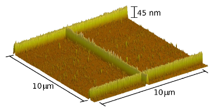
The research related to mesoscopic superconducting is limited by the fabrication technology. In particular case of QPS effect, to reach the regime of interest the nanowire should have very small cross-section. For example for aluminum the cross-section below 10 nm (still maintaining the high level of uniformity!) is mandatory [9]. Following Eq. (1), for materials like Nb, Sn or Pb with relatively high critical temperature one gets even more pessimistic estimations approaching 1 nm scale. This note explains why in particular case of niobium no traces of the QPS effect have been observed down to 7 nm scales [22]. With proper material selection the extremely tough fabrication requirements can be somehow relaxed. From our previous studies we have already learnt that in titanium the QPS effect is observable at sub-40 nm scales [11, 14], which is achievable with the standard e-beam lithography technique. In addition, titanium is an easy to work material and the extended microscopic and elemental analysis reveals no severe structural defects or/and impurities [11]. For the purpose of the present work we prepared several titanium nanowires with length and the effective diameter between 27 and 48 nm. The structures were fabricated with the standard lift-off e-beam lithography, and the titanium was deposited in UHV e-beam evaporator at residual pressure mbar. The substrate covered with exposed PMMA/MAA mask was cleaned with low-energy plasma immediately before the metal evaporation. Based on the measured resistivity , which is comparable with the tabulated value for the clean bulk titanium, the quality of the metal thin film is acceptable. Previous TEM and TOF-ERDA analyses of titanium nanostructures fabricated using identical conditions and parameters confirmed the high material quality: the highest concentration of foreign inclusions inside the titanium matrix corresponds to of oxygen [11]. This low concentration of impurities, combined with TEM analysis, disables any speculations about the presence of sample inhomogeneities capable to significantly broaden the dependence. The SPM analysis of the studied samples (Figure 1) confirmed the ’standard’ sample quality with the surface roughness of about several nm [11, 14, 23, 24]. The mean free path for the wire can be evaluated from the measured normal state resistance and the known material constant varying slightly in different literature sources. For our samples estimations give the mean free path 1 to 2 nm. The result agrees well with the SPM and TEM measured grain size of roughly 2 to 3 nm.
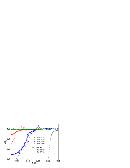
The measurements (Figure 2) were made employing the conventional four-probe configuration using 7 Hz lock-in technique at rather small excitation currents of about 50 pA. The experiments were made in dilution refrigerator with the base temperature down to 17 mK. All input/output lines were carefully protected from the noisy electromagnetic environment utilizing multi-stage RLC filtering enabling the electron temperature 35 mK at a base (phonon) temperature 20 mK [25]. For sufficiently thick nanowires with the effective diameter 40 nm the shape of the dependencies follows our earlier findings: pronounced superconducting transition with the low temperature data which can be described by the QPS model [12] with the realistic set of fitting parameters [11]. However the thinner the sample, the less the resistance drops below the certain ’critical temperature’ (Figure 2). It should be noted that for titanium the critical temperature decreases with the decrease of the cross-section . The size dependence of the critical temperature for low dimensional superconductors is a well-known effect, though the commonly accepted explanation of the phenomenon still does not exist [26, 27]. Thus the accurate experimental definition of the critical temperature for the thinnest samples , necessary for the theory fitting (Equation 1), is rather problematic due to the strongly broadened transition. Nevertheless for the thinnest samples 35 nm no set of realistic QPS model parameters can fit the experimental data (Figure 2). For these ultra-thin samples the experimental dependency is so weak, that the model [12] applicability criterion is not satisfied down to the lowest experimentally obtainable temperatures.
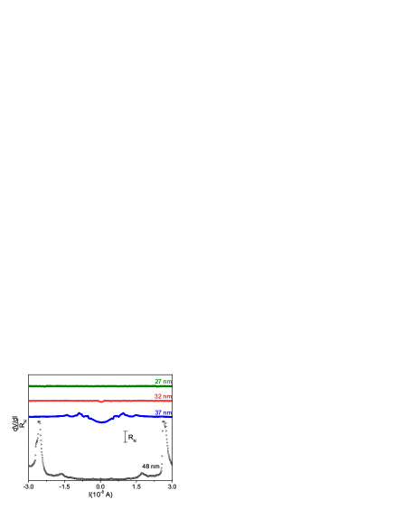
At temperatures well-below the critical temperature the dependencies (Figure 3) for the thickest studied samples demonstrate the conventional destruction of the zero-resistance state by current with the well-pronounced critical current . The double shape of the transition (e.g. at 22 nA and 28 nA for the 48 nm sample) presumably originates from slightly different effective cross-section of the samples at the node regions. With decrease of the nanowire cross-section, as expected from the dependencies, the the zero-resistance state disappears and only some residual ’critical current’ peculiarities can be traced. In the thinnest samples the zero-biased differential resistance very slightly increases indicating the presence of a weak Coulomb blockade. Observation of a pronounced Coulomb effects requires the true current biasing (including the high frequencies!) [19] and this experimental realization is not within the scope of the present paper.
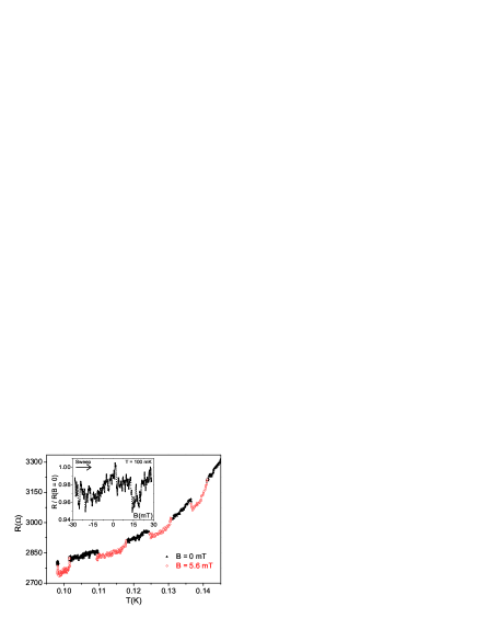
Yet one more interesting observation is the negative magnetoresistance (nMR) which is observed in the thinnest samples with pronounced QPS contribution (Figure 4). The effect increases with lowering the temperature. Similar phenomenon has been reported in aluminum [10], niobium and [28] and lead [29] nanowires. The origin of the nMR in these quasi-1D channels is still under debates. In case of niobium and it was conjected that some rogue magnetic moments might be present, and their pair breaking contribution, active at lower magnetic fields, is suppressed by higher fields leading to the observed nMR [28]. However this mechanism needs an independent proof of the existence of these magnetic moments, and cannot explain the nMR in such material as aluminum [10], where it is a well-known fact that majority of magnetic impurities can obtain a non-negligible magnetic moment only at relatively high concentrations [30]. Another explanation of the nMR phenomenon deals with the magnetic field suppression of the charge imbalance accompanying each phase slip event [31]. Somehow related mechanism, capable to provide nMR, deals with more effective suppression of superconductivity in (wider) electrodes affecting the phase slip formation in the (thinner) nanowire [32].
4 CONCLUSIONS
and characteristics of titanium nanowires with sub-50 nm diameters were measured. The shape of the dependencies for the ’not-too-narrow’ samples with the effective diameters 40 nm confirms the earlier findings: pronounced superconducting transition with the low temperature data which can be described by the quantum phase slip model [12]. In thinner samples the transitions dramatically flatten disabling any comparison with the existing fluctuation models, which assume that the phase slips are still the rare events and hence the effective resistance should be much smaller than the normal state resistance. The dependencies confirm the data conclusion about the absence of the truly zero-resistance state in the thinnest samples. The negative magnetoresistance is observed, while the origin of the effect is not clear.
References
References
- [1] Little W A Decay of persistent currents in small superconductors Phys. Rev., 156:396–403, 1967.
- [2] Langer J S and Ambegaokar V Intrinsic resistive transition in narrow superconducting channels Phys. Rev., 164:498–510, 1967.
- [3] McCumber D E and Halperin B I Intrinsic resistive transition in thin superconducting wires driven from current sources Phys. Rev., 172:427–429, 1968.
- [4] Lukens J E, Warburton R J and Webb W W Onset of quantized thermal fluctuations in ”one-dimensional” superconductors Phys. Rev. Lett., 25:1180–1184, 1970.
- [5] Newbower R S,Beasley M R, and Tinkham M Fluctuation effects on the superconducting transition of tin whisker crystals Phys. Rev. B, 5:864–868, 1972.
- [6] Giordano N Evidence for macroscopic quantum tunneling in one-dimensional superconductors Phys. Rev. Lett., 61:2137–2140, 1988.
- [7] Bezryadin A, Lau C N and Tinkham M Quantum suppression of superductivity in ultrathin nanowires Nature, 404:971–974, 2000.
- [8] Altomare F, Chang A M, Melloch M R, Hong Y, and Tu C W Evidence for macroscopic quantum tunneling of phase slips in long one-dimensional superconducting Al wires Phys. Rev. Lett., 97:017001, 2006.
- [9] Zgirski M , Riikonen K-P, Touboltsev V, and Arutyunov K Yu Size dependent breakdown of superconductivity in ultranarrow nanowires Nano Letters, 5(6):1029–1033, 2005.
- [10] Zgirski M, Riikonen K P, Touboltsev V, and Arutyunov K Yu Quantum fluctuations in ultranarrow superconducting aluminum nanowires Phys. Rev. B, 77:054508, 2008.
- [11] Lehtinen J S, Sajavaara T, Arutyunov K Yu, Presnjakov M Yu, and Vasiliev A L Evidence of quantum phase slip effect in titanium nanowires Phys. Rev. B, 85:094508, 2012.
- [12] Zaikin A D, Golubev D S, van Otterlo A, and Zimányi G T Quantum phase slips and transport in ultrathin superconducting wires Phys. Rev. Lett., 78:1552–1555, 1997.
- [13] Arutyunov K Yu, Golubev D S, and Zaikin A D Superconductivity in one dimension Physics Reports, 464(1):1 – 70, 2008.
- [14] Arutyunov K Yu, Hongisto T T, Lehtinen J S, Leino L I, and Vasiliev A L Quantum phase slip phenomenon in ultra-narrow superconducting nanorings Sci.Rep., 2:213, 2012.
- [15] Astafiev O V, Ioffe L B, Kafanov S, Pashkin Yu A, Arutyunov K Yu, Shahar D, Cohen O, and Tsai J S Coherent quantum phase slip Nature, 484:355–358, 2012.
- [16] Mooij J E and Nazarov Yu V Superconducting nanowires as quantum phase-slip junctions Nature Physics, 2:169–172, 2006.
- [17] Hriscu A M and Nazarov Yu V Model of a proposed superconducting phase slip oscillator: A method for obtaining few-photon nonlinearities Phys. Rev. Lett., 106:077004, 2011.
- [18] Hriscu A M and Nazarov Yu V Coulomb blockade due to quantum phase slips illustrated with devices Phys. Rev. B, 83:174511, 2011.
- [19] Hongisto T T and Zorin A B Single-charge transistor based on the charge-phase duality of a superconducting nanowire circuit Phys. Rev. Lett., 108:097001, 2012.
- [20] Averin D V, Zorin A B, and Likharev K K Coherent oscillations in small tunnel junctions Zh. Eksp. Teor. Fiz., 88:692–703, 1985.
- [21] Kuzmin L S and Haviland D B Observation of the bloch oscillations in an ultrasmall josephson junction Phys. Rev. Lett., 67:2890–2893, 1991.
- [22] Rogachev A and Bezryadin A Superconducting properties of polycrystalline Nb nanowires templated by carbon nanotubes Applied Physics Letters, 83(3):512–514, 2003.
- [23] Savolainen M, Touboltsev V, Koppinen P, Riikonen K P, and Arutyunov K Yu Ion beam sputtering for progressive reduction of nanostructures dimensions Applied Physics A, 79:1769–1773, 2004.
- [24] Zgirski M, Riikonen K-P, Tuboltsev V, Jalkanen P, Hongisto T T, and Arutyunov K Yu Ion beam shaping and downsizing of nanostructures Nanotechnology, 19(5):055301–1–055301–6, 2008.
- [25] Arutyunov K Yu, Auraneva H-P, and Vasenko A S Spatially resolved measurement of nonequilibrium quasiparticle relaxation in superconducting Al Phys. Rev. B, 83:104509, 2011.
- [26] Shanenko A A, Croitoru M D, Zgirski M, Peeters F M and Arutyunov K Yu Size-dependent enhancement of superconductivity in Al and Sn nanowires: Shape-resonance effect Phys. Rev. B, 74:052502, 2006.
- [27] Oreg Y and Finkel’stein A M Suppression of in superconducting amorphous wires Phys. Rev. Lett., 83:191–194, 1999.
- [28] Rogachev A, Wei T C, Pekker D, Bollinger A T, Goldbart P M and Bezryadin A Magnetic-field enhancement of superconductivity in ultranarrow wires Phys. Rev. Lett., 97:137001, 2006.
- [29] Xiong P., Herzog A V and Dynes R C Negative Magnetoresistance in Homogeneous Amorphous Superconducting Lead Wires Phys. Rev. Lett., 78:927, 1997.
- [30] Jalkanen P, Touboltsev V, Koivisto H, Suominen P, Suppula T, Arutyunov K Yu, and Raisanen J Superconductivity suppression in Fe-implanted thin Al films Journal of Apllied physics, 98(1):016105, 2005.
- [31] Arutyunov K Yu Negative magnetoresistance of ultra-narrow superconducting nanowires in the resistive state Physica C: Superconductivity, 468(4):272 – 275, 2008.
- [32] Vodolazov D Y Negative magnetoresistance and phase slip process in superconducting nanowires Phys. Rev. B, 75:184517, 2007.