Electronic Transport Through EuO Spin Filter Tunnel Junctions
Abstract
Epitaxial spin filter tunnel junctions based on the ferromagnetic semiconductor europium monoxide, EuO, are investigated by means of density functional theory. In particular, we focus on the spin transport properties of Cu(100)/EuO(100)/Cu(100) junctions. The dependence of the transmission coefficient and the current-voltage curves on the interface spacing and on the EuO thickness is explained in terms of the EuO density of states and the complex band structure. Furthermore we also discuss the relation between the spin transport properties and the Cu-EuO interface geometry. The level alignment of the junction is sensitively affected by the interface spacing, since this determines the charge transfer between EuO and the Cu electrodes. Our calculations indicate that EuO epitaxially grown on Cu can act as a perfect spin filter, with a spin polarization of the current close to 100%, and with both the Eu-5 conduction band and the Eu-4 valence band states contributing to the coherent transport. For epitaxial EuO on Cu a symmetry filtering is observed, with the states dominating the transmission. This leads to a transport gap larger than the fundamental EuO band gap. Importantly the high spin polarization of the current is preserved up to large bias voltages.
pacs:
71.20.-b, 71.20.Be, 75.50.Pp, 72.25 DcI Introduction
Magnetic tunnel junctions using MgO as a tunnel barrier generally display large tunneling magneto resistance (TMR) and they are now widely used in read heads for ultra high-density hard-disk drives as well as in random access memory devices S.Yuasa . Currently a room temperature TMR ratio as high as 500% can be reached in junctions made of polycrystalline Fe (more precisely CoFeB) sandwiching a thin MgO insulating layer S.X.Huang . Despite such huge TMR ratios the Fe/MgO system presents two limiting aspects for future applications. Firstly, there is no flexibility on the materials side, which means that high TMR ratios are achieved only for the Fe/MgO combination and only for a particular crystal orientation, (100). Furthermore high crystallinity is needed as the electrodes themselves carry only a moderate spin-polarization of the conduction electrons. Secondly, the TMR consistently decreases with increasing the applied voltage and/or the temperature and so the operation of a practical device utilizing a magnetic tunnel junction is limited to low bias J.S.Moodera-2007 .
The origin of the high TMR found in Fe/MgO-based junctions is rooted in the spin filtering effect Butler-2001 ; Mathon that MgO exerts on the conduction electrons injected from the Fe electrodes Ivan-2009 ; C.Heiliger-2006 ; Itoh ; C.Tiusan-2007 ; W.H.Butler-2008 ; G.X.Miao-2009 ; G.X.Miao-2011 . Only electrons with specific symmetry and with small transverse momentum contribute significantly to the current. For energies around the Fermi energy, , these are found only in the majority Fe states. As a consequence of this symmetry filtering the decay rate of the conduction electron wave-function into the MgO barrier of the majority spins is smaller than that of the minority ones C.Tiusan-2007 . These decay rates are determined by the complex band structure (CBS) of the tunnel barrier Butler-2001 ; Mathon . A crucial feature of the symmetry spin filtering effect is that TMR ratios larger than 1000% can be achieved, despite the fact that the spin-polarization of the electrodes is only around 65% (for CoFeB).
Another possible strategy for obtaining a spin filter effect, and thus very large TMR ratios, is that of using a ferromagnetic insulator as spacer between the metallic electrodes. In this case the energy barrier has a different height for majority and minority spins, which leads to the suppression of the current for one of the two spin-species for thick enough junctions. The tunnel current density is proportional to the energy-dependent transmission coefficient through the barrier, , which itself depends exponentially on the barrier height, , and the barrier thickness, . This can be written as , with , with being the electron mass. Clearly if the barrier height is different for the different spin-species the current polarizations will increase exponentially with the insulating layer thickness, leading to full spin polarization for thick barriers J.S.Moodera-2007 ; G.X.Miao-2011 . Devices constructed with this principles are called spin filter tunnel junctions (SFTJs). The quest for manufacturing SFTJs then reduces to that of finding suitable ferromagnetic semiconductors.
The europium chalcogenides EuS, EuSe and EuO have all a rocksalt structure and they are all ferromagnetic insulators. Among these EuO presents the largest conduction band exchange splitting, 0.54 eV, below the material’s Curie temperature of 69 K A. Mauger ; Steeneken-2002 ; J.S.Moodera-2004 . In EuO the divalent Eu ions possess a large local moment originating from the half-filled 4 band (). An energy gap of 1.1 eV separates the half-filled majority Eu-4 band from the Eu-5 conduction band J.S.Moodera-2007 . SFTJs based on polycrystalline EuO in the form of a metal/EuO/metal heterojunction have been studied in several recent experiments J.S.Moodera-2004 ; E.Negusse-J.Appl-2006 ; SANTOS-2008 ; Watson-2008 ; E.Negusse-J.Appl-2009 ; Martina-J.Appl-2009 ; Martina-Europhys-2009 . However, the spin transport properties of crystalline epitaxial EuO junctions have not been studied theoretically so far. The purpose of this paper is to provide such theoretical insight. In particular we present ab-initio results for the electronic structure and the electron transmission through EuO barriers sandwiched between Cu electrodes oriented along the [001] direction.
Our paper is organized as follows. We start our discussion by presenting the methods used and the structure of the device investigated. Then, in the following section we present the electronic structure of EuO and its complex band structure along the [001] direction. This determines the spin-dependent decay rates and thus the spin filter efficiency. In section IV we discuss the transmission coefficient at zero bias, while in section V the dependence of the spin transport on the EuO thickness is analyzed and related to the complex band structure. The current-voltage, -, characteristics are discussed in the following section, where we find that, in contrast to Fe/MgO junctions, the polarization of the current is not reduced by the applied bias. Finally we conclude.
II Methods
The EuO and Cu electronic structures are calculated by using the ab-initio density functional theory (DFT) code SIESTA siesta . Since the local density approximation (LDA) is not sufficient to give an accurate description of the EuO density of states (DOS), we correct for on-site Coulomb repulsion with an LDA+U treatment anis91 ; anismov93 . Following Ref. [ingle08, ], the exchange constant and the on-site orbital potential for the Eu-4 orbitals are set respectively to eV and eV, while for the O-2 orbitals we use eV and eV. Troullier-Martins norm-conversing relativistic pseudopotentials are used for Cu, Eu and O. The wave functions are expanded over a double plus polarization basis set (DZP), except for the Eu-4 states, for which we use single-. An equivalent real space mesh cutoff of 600 Ry is used together with an electronic temperature of 69 K. We sample the Brillouin zone (BZ) in the plane perpendicular to the transport direction over a -point uniform mesh.
Spin transport is studied by using the SMEAGOL electronic transport code Smeagol1 ; Rocha ; Ivan , which combines DFT with the nonequilibrium Green’s functions (NEGF) technique. SMEAGOL uses the Hamiltonian matrix provided by SIESTA to calculate the charge density so that the same pseudopotentials and exchange and correlation function can be used for both the electronic structure and the transport. The spin current at each bias voltage is calculated by energy integration of the spin-dependent transmission coefficient ,
| (1) |
where is the spin index (), is the Fermi function, is the applied bias voltage and the electron charge. The total transmission coefficient is obtained by integrating the -dependent transmission over the 2-dimensional BZ perpendicular to the transport direction,
| (2) |
where is the area of the BZ. We denote as the zero bias transmission coefficient. In our calculations we assume the lattice structure to be periodic in the - plane, and we keep the transport direction along the -axis. While -points are enough to accurate converge the charge density, the presence of resonances in requires the much larger mesh of to evaluate the transmission coefficient both for zero and finite bias. The - characteristics are calculated non-self-consistently by evaluating the transmission coefficient over an effective bias-dependent Hamiltonian matrix, which in turns is obtained by adding a rigid shift to the zero bias Hamiltonian matrix elements of the electrodes and a linear potential across the insulating barrier. This is a good approximation to the self-consistent potential drop for tunnel junctions Ivan-2009 , which appears essentially like that of a standard parallel plate capacitor.
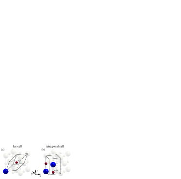
EuO crystallizes in the rocksalt structure with a lattice constant of Å. The primitive face-centered cubic (fcc) unit cell containing one Eu and one O atom is shown in Fig. 1(a). Since we consider transport along the [001] direction, we have to use as basic building block for the EuO spacer a cell with size and orientation different from that of the primitive one. The smallest possible cell thus has tetragonal symmetry, and contains 2 Eu and 2 O atoms [see Fig. 1(b)]. By stacking multiples of such tetragonal cells along the -direction we can construct barriers of arbitrary thickness, where one cell contains 2 EuO monolayers (MLs).
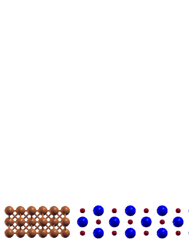
The model spin filter junction considered here consists of MLs of EuO sandwiched between non-magnetic Cu electrodes, being an integer. As electrodes material we consider fcc Cu oriented along the [001] direction (lattice constant 3.61 Å), a material choice which has been adopted in several experiments E.Negusse-J.Appl-2006 ; SANTOS-2008 ; Watson-2008 ; E.Negusse-J.Appl-2009 . When the tetragonal EuO unit cell is used the lattice constant of Cu can be matched with only a slight strain to the EuO lattice, since the dimensions along and are Å. The junction setup is illustrated in Fig. 2. In this basic setup both the O and Eu atoms are placed over the hollow sites of the Cu surface. We also perform calculations for EuO shifted in the - plane. However the transport and spin filter properties are not sensitively dependent on such a shift. The equilibrium interface distance, , between Cu and EuO is found to be = 2.8 Å. Note that we do not consider possible oxidation at the Cu/EuO interface, or the formation of secondary EuO phases.
III EuO electronic structure
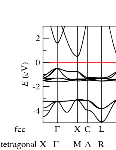
Let us start our discussion by describing the electronic structure of EuO. The calculated EuO band structures for both the primitive fcc and the tetragonal unit cells are presented respectively in Figs. 3 and 5. The results agree rather well with previously published calculations ingle08 ; D.B.Ghosh . In order to compare the band structures for two cells we use the same -space path. Standard high-symmetry points are specified for the primitive fcc BZ and also for the primitive tetragonal BZ (where applicable). We note that due to band-folding for the tetragonal cell we find twice the number of bands than for the primitive fcc one. The X point [located at (/aEuO,0,0)] and the X′ point [located at (0,0,/aEuO)] are equivalent in the fcc BZ. However for the tetragonal cell they are independent since the X′ point is equivalent to in the tetragonal cell. There is a band gap of about 1.0 eV for majority spins (Fig. 3), whereas the gap increases to about 3.5 eV for the minority ones. For the primitive fcc cell (Fig. 3) we find an indirect gap, where the top of the valence band is at and the bottom of the conduction band at X′ point. This gap become direct when the primitive tetragonal cell is used due to band-folding (Fig. 5). Note that the tetragonal cell is the relevant one for the transport so that EuO along the [001] direction behaves as a direct gap ferromagnetic semiconductor.
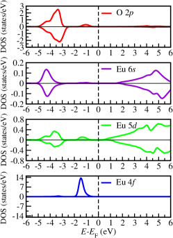
The majority spins the energy spectrum consists of three parts: the conduction bands, the top valence bands, and the lower valence bands. The top valence bands are found in the range between eV and eV (we set the energy zero approximately to the middle of the gap). It is clearly seen from Fig. 4, where we show the projected DOS (PDOS) on different orbitals, that the main character of the top valence band is given by the Eu-4 states. While many of the Eu-4 bands show very little dispersion, indicating strong localization, in EuO the Eu-4/O-2 mixing leads to a significant dispersion around the point. This is an indication of delocalized states. We note that at the top of the valence band Eu-4 and O-2 contribute approximately equally to the density of states. In addition, the hybridization leads to a large contribution to the inter-site coupling of kinetic processes KUNES . We therefore expect such delocalized states to contribute significantly to the transport through a EuO barrier. Below the top valence bands, the bottom valence bands are observed in the energy range from eV to eV. It is seen from Fig. 3 that the bottom valence bands are dominated by O-2 states. The bandwidth of the O-2 states (1.9 eV) is not much larger than the one of the Eu-4 ones (1.1 eV), which indicates a similar wave-function delocalization. The energy gap between the top valence and bottom conduction bands is about 1.7 eV. The lower conduction bands are dominated by Eu-5 states. Above 1.6 eV we find also contributions from the Eu-6 orbitals. We note that the DOS at the lower end of the conduction bands is very small, which is due to a high dispersion.
Next we consider the electronic band structure of the minority spins. The empty Eu-4 states start at around 11.1 eV, so that they are not expected to affect the transport properties. As for the majority states, the conduction bands are dominated by Eu-5 and Eu-6 orbitals, while the valence bands are dominated by O-2. The spin filter character of EuO is due to a spin splitting of the bands, which leads to a difference in the band gaps for the majority and minority spins. The splitting between the majority and minority spin conduction bands is calculated to be about 0.6 eV, in agreement with previous theoretical studies ingle08 ; D.B.Ghosh ; KUNES ; Miyazaki-2008 ; Bousquet-2010 ; J.M.An-2011 and with recent experiments using 3D angle resolved photoemission spectroscopy Miyazaki-2009-Jpn ; Miyazaki . The Eu-6 states show a similar spin splitting as the Eu-5 states, namely 0.4 eV.

We now analyze the symmetries of the different bands. Symmetries are important for the transport through epitaxial tunnel junctions Butler-2001 ; N.M.Caffrey-2011 , since, at any given energy, only evanescent states in the insulating barrier with matching symmetry with propagating Bloch states in the electrodes can contribute to the conductance. Since the EuO gap in the tetragonal cell is at , the transport will be dominated by states close to , denoted as , for which the barrier height is smallest (the coordinate system is defined in Fig. 1). In the energy range comprised between eV and eV around the Cu electrodes have only states of symmetry with respect to the -axis. For a cubic space group, the symmetry transforms as a linear combination of 1 (-orbitals), ( orbitals), ( orbitals), and ( orbitals). Above 1.6 eV the Cu states have symmetry. The symmetry transforms as a linear combination of ( orbitals), ( orbitals), ( orbitals) and ( orbitals). At energies below eV we find the Cu-3 orbitals, so that there are also states with different symmetries. For a transport measurement up to about 2 V we therefore expect the states with symmetry to determine the transport properties.
In order to investigate in more details the propagating and evanescent states in the EuO barrier we calculate the complex band structure (Fig. 6) at Butler-2001 ; N.M.Caffrey-2011 ; ddtcormac and analyze the symmetries of the evanescent states. Real wave vectors () represent propagating states and complex wave vectors ( represent evanescent states, since their wave functions decay as across the barrier. For the majority spins the top of the valence band is three-fold degenerate, with one state with symmetry (Eu-4 and O-2 orbitals) and two states with symmetry. Since the state with symmetry has a lower effective mass than those with symmetry, the corresponding evanescent states have smaller , and therefore a slower decay. The bottom of the conduction band is given by a state with symmetry (Eu-5 orbital). At 1.6 eV we find the Eu-4 states, which have symmetry. Therefore for the band forms a semi-circle between the Eu-4 states at the top of the valence band and the Eu-4 states at 1.6 eV.
Consequently, we expect the tunneling transmission to be dominated by the states in this energy range. The Eu-5 propagating states with symmetry cannot couple to the Cu states, and therefore are not expected to contribute significantly to the transmission. For and different from zero the Eu-5 states are no longer fully orthogonal to the Cu-4 states. However, since the gap increases with increasing and , the barrier height for such states is larger. Hence their contributions to the total transmission are smaller. Overall one expects a rather weak coupling to the Cu-4 states and a low transmission for states at the bottom of the EuO conduction band.
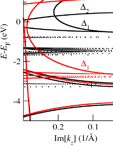
In the minority spins bands there are also three degenerate states at the top of the valence band, one with symmetry (O-2 orbital) and two with symmetry (O-2 and O-2 orbitals). The state again has lower effective mass and therefore a smaller decay for evanescent states. At the bottom of the conduction band the symmetries are analogous to those of the majority spins. We therefore also expect the minority conductance to be dominated by the symmetry. However, since the minority band gap is much larger than that of the majority spins, is also significantly larger for states in the gap. As a consequence, we expect to be substantially larger than . This is usually attributed only to different energies of the bottom of the conduction band J.S.Moodera-2007 , whereas our complex band structure analysis indicates that the decay of the evanescent states has significant contributions also from states in the valence band, especially for the majority spins. We note that the Eu-5 states will contribute to the transport if different electrodes, possessing symmetry states in the relevant energy range, are used
IV Spin transport properties of the EuO junction at zero bias
In this section we analyze the zero bias transport properties of Cu/EuO/Cu junctions by taking as an example a stack containing 9 MLs of EuO ( Å). The energy level alignment between the metal and the insulator is an important factor determining the transport properties of the junction. To a first approximation, one can estimate the alignment by comparing the workfunctions, , of the two components. The workfunctions of EuO and Cu are calculated by using the Hartree electrostatic potential, , as the reference potential Ivan-2010 . We define as the difference between and the vacuum potential of a Cu slab, while is given by the difference between and the energy of the valence band top of a EuO slab, . We calculate eV and eV, both values in good agreement with the experimental values, respectively ranging between 4.5 eV to 5.1 eV for Cu, and being 1.7 eV for EuO D.E. Eastman . Since , electron transfer from EuO to Cu can be expected at the interface, leading to the pinning of the valence band top of EuO to the Cu . This is indeed the case for the equilibrium distance ( Å), where the Eu-4 states are located just below [see Fig. 7(c) and (d)].
In experiments investigating bias-dependent transport the actual junctions usually contain polycrystalline EuO, so that the interface between Cu and EuO is not well defined Martina-Europhys-2009 . In our calculations, in contrast, we assume a perfect epitaxial interface and do not explicitly consider the formation of defects, oxidation of Cu, or the possible formation of Eu2O3 at the interface E.Negusse-J.Appl-2006 ; Martina-J.Appl-2009 . The effect of such modifications of the interface on the electronic structure are manyfold, the most important being that they usually lead to a different charge transfer and therefore to a different band alignment between Cu and EuO. In practice this means that (depending on the detailed structure of the interface, which is determined by the experimental conditions) can be placed at different positions across the EuO gap. In our calculations we can tune the charge transfer and consequently the position of in the EuO gap by modifying the distance, , between Cu and EuO at the interface. We find that decreasing the distance from the equilibrium one, i.e., increasing the coupling between Cu and EuO, the EuO states shift to lower energies with respect to . For Å is located approximately in the middle of the gap [see Fig. 7(a) and (b)], while for Å it is pinned at the EuO conduction band minimum (not shown). Therefore, Å can be used to simulate the transport properties of n-type EuO, as obtained for O-deficient barriers M.Barbagallo ; X.Wang ; J.A.C.Santana . In the remaining part of this paper we will present the transport properties for both Å and Å, in order to illustrate the effect of a shift of induced by interface modifications. Importantly, we will demonstrate that, for any position of , EuO always shows excellent spin filter characteristics up to high bias voltages. We note that if experimentally a perfect epitaxial junction can be realized, the measurements should correspond to our results for the equilibrium distance Å.
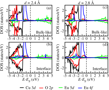
In Fig. 7 we compare the PDOS of atoms at the Cu/EuO interface with the PDOS of atoms at a maximal distance from the interface (to be considered bulk-like). While the two PDOSs are similar for most atomic orbitals, there is a significant difference for the O-2 states. At the interface the O-2 states extend over a larger energy range as compared to bulk-like atoms, indicating a coupling to the Cu substrate. In fact, for Å the broadening is more pronounced than for Å, which is due to the larger coupling. The PDOS in the middle of the EuO layer is very similar to that of bulk EuO, indicating that in the middle of the junction one recovers the bulk electronic structure of EuO. Although in Fig. 7 only the fully occupied Cu-3 states are shown, we note that the Cu-4 states determine the transport properties of the electrodes, since they have an approximately constant PDOS in a large energy range around . In Fig. 7 the Cu-4 PDOS is not shown, since it is not visible on the chosen scale.
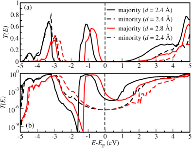
The zero bias transmission coefficient for different is shown in Fig. 8 [on a linear scale in panel (a) and on a logarithmic scale in panel (b)]. Due to the shift of the electronic states for different (see Fig. 7), is shifted towards higher energies for Å as compared to Å, while there is only a minor change in the height of the different transmission peaks. It can be seen that has two small gaps for the majority spins and one large gap for the the minority ones. For the minority spins the conduction occurs only through the O-2 states for energies below eV and through the Eu-5 and Eu-6 states for energies above about 2 eV. In contrast, for the majority spins the Eu-4 states just below also contribute significantly to the conductance. This is consistent with the band structure, which shows that the Eu-4 states hybridize with the O-2 and are rather delocalized. The result of such hybridization is a large majority transmission in the energy range between eV and . Therefore, for all energies below (down to about eV) the transmission of the majority spins is much larger than that of the minority ones. For energies above (up to about 2 eV) it is also significantly larger. This is due to fact that the Eu-5 conduction band minimum is located about 0.6 eV lower in energy for the majority spins than for the minority ones (Fig. 6).
The overall result hence is that for any position of in the EuO gap we expect a very high spin-polarization of the current. This should persist up to high bias voltages (of the order of the energy for which the transmission of the majority spins is much larger than that of the minority ones). The spin-filtering efficiency at small applied bias is defined as Shen . Since is about two to three orders of magnitude larger than , we have a spin filter efficiency close to 100%, indicating that the EuO barrier is an almost perfect spin filter. We note that the extremely high efficiency is obtained for defect-free epitaxial junctions. Such value might be reduced by defects in the EuO barrier as well as for polycrystalline EuO. Nevertheless one can expect that also in these cases the spin-filter efficiency may remain high.
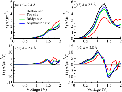
In order to investigate the dependence of the spin transport properties on the geometry of the Cu/EuO interface we calculate for different positions of EuO with respect to Cu. So far we have considered a setup in which O is placed on top of the hollow site of the Cu surface. We compare the results with the following three geometries: 1) O placed on top of Cu, 2) O placed on the bridge site between two Cu atoms, and 3) O placed at an arbitrary low symmetry site. The equilibrium distance is 2.8 Å for all cases and the total energies are similar, with the bridge site having the lowest energy. In Fig. 9 we show calculated for the different sites, for both Å and Å. Overall the changes in transmission corresponding to the different sites are rather small, a fact, which indicates that the geometry of the Cu/EuO surface does not significantly affect the band alignment and transport properties of the junction.

At the bottom of the conduction band there are some quantitative differences in transmission between the different sites. This is due to the fact that shifting the O atom with respect to Cu alters the coupling between the Cu-4 and Eu-5 states. As discussed in Section III, while the states on the top of the valence band couple well to the Cu band, the states at the bottom of the conduction band couple only slightly to these states due to a symmetry mismatch. This is also the reason for the fact that the transmission gap is somewhat larger than the EuO band gap, and for the slow increase of the transmission at the bottom of the conduction band with energy. For the bridge and low symmetry sites the symmetry mismatch is slightly reduced, resulting in a somewhat smaller transmission gap. Since the results for the different sites are very similar, we will only consider the hollow site in the remaining of the paper.
V Thickness dependence of the conductance
In this section we analyze the effect of the EuO thickness, , on the spin transport properties of the Cu/EuO/Cu junction. The transmission spectra for different EuO thicknesses, and for both Å and Å, are shown in Fig. 10. From the figure it can be seen that the band alignment is not affected by the thickness, while the transmission in the gap decreases exponentially with it. Since for energies in the gap we have , we can estimate from the change of with increasing . Indeed can be calculated from evaluated at two different thicknesses and as
| (3) |
where and are the transmissions for and , respectively.
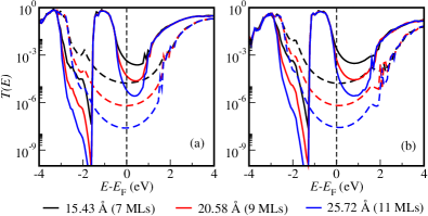
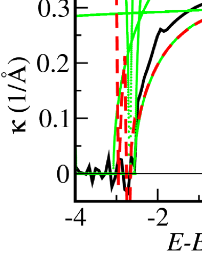
In Fig. 11 we show the calculated (solid lines), evaluated for Å (9 EuO MLs) and Å (11 EuO MLs). For energies within 1.5 eV around , is significantly smaller than . Therefore, increasing the EuO layer thickness leads to an enhancement of the ratio between the transmissions of the majority and minority spins, i.e., to an increase of the spin filtering efficiency. For Å, is larger than zero in the range from eV to 1.0 eV (resulting in a transmission gap of 1.5 eV), whereas is larger than zero in the range from eV to 1.6 eV (resulting in a transmission gap of 4.2 eV). For Å, is shifted to higher energies, and the transmission gap amounts to about 1.7 eV for the majority spins and 4.7 eV for the minority ones. While shows a parabolic behavior for energies close to the valence band top, for the conduction band minimum the behavior is less well defined. This is due to the symmetry mismatch between the Cu states and the conduction band Eu-5 states, see Sec. IV. Nevertheless the barrier height is about 0.6 eV larger for the minority spins as compared to the majority ones for transmission through the conduction band. For the transmission through the valence band the difference is even larger, since there are no filled minority spin Eu-4 states.
In Fig. 11 we also present the obtained from the transmission only at the point (dashed curve). Close to the valence band the wave-function decay is similar to the previous case, which shows that is dominated by contributions around . However, for energies close to the conduction band, at is much larger than the total , which shows that here the transport occurs mainly at -points away from the BZ center. A comparison with the EuO complex bands (green curves; see Fig. 6 for a description of the symmetries) shows that, at , follows approximately for states. It is clear that no transmission occurs through the conduction band states. For -points away from the EuO states can couple to the Cu states, which leads to a decrease of the total above the conduction band minimum. For electrode materials with states above we expect the total to follow the complex bands at for energies below the conduction band minimum.
The barrier heights are calculated from the damping coefficient shown in Fig. 11. The values of and are determined as the lowest energy at which crosses zero in the conduction band for the majority and minority spins, respectively. Similarly, and are determined as the highest energy at which crosses zero in valence band for the majority and minority spins, respectively. By this method we obtain for Å the values eV, eV, eV, and eV. For Å we obtain eV, eV, eV, and eV. The exchange splitting for the conduction band of 0.6 eV matches the value for bulk EuO.
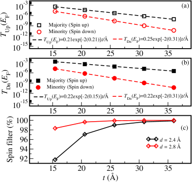
For the low bias conductance the thickness dependence of the transmission coefficient at is evaluated and from it the decay coefficient. In Fig. 12 we show at Å and Å as functions of the EuO thickness. The decay rates correspond to those obtained in Fig. 11 at . In Fig. 12(c) the effective spin filtering at is addressed. It can be seen that it increases towards 100% as increases.
VI The - curve of the EuO spin filter
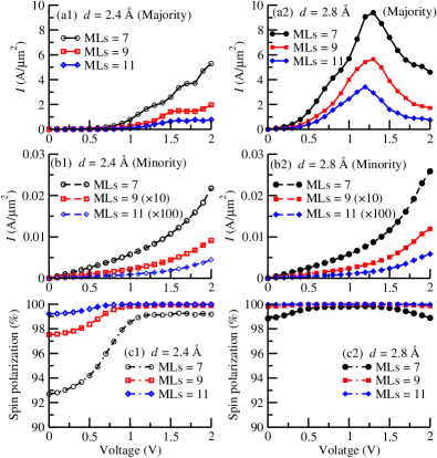
The spin-resolved current-voltage, -, characteristic and the spin polarization as functions of the bias voltage are shown in Fig. 13 for 7, 9 and 11 MLs of EuO, and for both and Å. The majority spin current is higher than the minority spin current for all bias voltages and for all thicknesses, leading to large polarization in all cases. At low bias there is a rapid increase of the tunneling current with the bias. This is typical for such systems due to the fact that the current is not only determined by electrons at but also by those in the energy range (bias window), for which the barrier height can be reduced up to about . At a bias of about 0.7 V for Å the electrons start to flow through the valence band top, so that there is a sharp increase in current. Since for Å the valence band is very close to , the onset is found at very low bias. The current increases up to about 1.3 V, above which a decrease with increasing bias is found. This is caused by a reduction of the transmission over the entire bias window once the bias is very large. Such a current reduction results from the enhanced scattering as the potential is tilted inside the barrier due to the applied bias voltage. In these large scattering conditions, incoherent contributions to the current (not included here) are expected to play an important role.
For the minority spins, in contrast, the current remains in the tunneling regime for all bias voltages due to the large barrier height. The large difference between majority and minority spin currents is reflected by a high spin polarization, , defined as [see Fig. 13(c1)]. remains large for all the bias voltages considered due to the small . We note that the spin splitting of the conduction band plays only a secondary role in our results, since the majority current is mainly determined by the valence band contribution (which is not sensitive to the exact position of inside the EuO energy gap). For n-type EuO one expects a pinning of the conduction band to , leading to an almost metallic-like character dominated by the EuO conduction electrons.
The dependence of the - characteristics and of the conductance trace on the Cu/EuO interface geometry is addressed in Fig. 14. Overall the - characteristics are similar for all the interfaces, which reflects the fact that the zero bias transmission is also rather similar (see Fig. 9). For Å there is a sharp increase in at the current onset, whereas it then stays approximately constant. For Å, in contrast, is large at low bias and changes sign at 1.3 V.
VII Conclusions
We have studied the electronic structure, the complex band structure and the spin transport properties of epitaxial Cu/EuO/Cu tunnel junctions. The spin transport properties of EuO epitaxially grown on Cu are dominated by the Eu-4 valence states and by the Eu-5 conduction states. We show that EuO acts as an almost perfect spin filter, where close to 100% spin polarization can be achieved. The polarization increases with increasing EuO thickness as expected from the complex band structure, where the decay of the wave function into EuO is predicted to be much smaller for the majority spins than for the minority ones. Since the conduction states of EuO have no symmetry to match the states in the Cu electrodes, the gap in the transmission coefficient is significantly larger than the band gap of EuO. Under a bias voltage the spin polarization of the current does not decrease, as in usual tunnel junctions, but remains approximately constant up to all considered bias voltages. This opens promising perspectives of using EuO for device applications.
VIII Acknowledgements
We would like to acknowledge technical assistance from Apirat Siritarathiwat and Hao Wang. N. J. and U. E. acknowledges financial support by the Deutsche Forschungsgemeinschaft through TRR 80. Computational resources have been provided by TCHPC Ireland and LRZ Munich, Germany. I. R. and S. S. acknowledge financial support by KAUST (ACRAB project).
References
- (1) S. Yuasa, and D. D. Djayaprawira, J. Phys. D: Appl. Phys. 40, R337 (2007).
- (2) S. X. Huang, T. Y. Chen, and C. L. Chien, Appl. Phys. Lett. 92, 242509 (2008).
- (3) J. S. Moodera, T. S. Santos, and T. Nagahama, J. Phys.: Condens. Matter 19, 165202 (2007).
- (4) W. H. Butler, X.-G. Zhang, T. C. Schulthess, and J. M. MacLaren, Phys. Rev. B 63, 054416 (2001).
- (5) J. Mathon and A. Umerski, Phys. Rev. B 63, 220403(R) (2001).
- (6) I. Rungger, O. Mryasov, and S. Sanvito, Phys. Rev. B 79, 094414 (2009).
- (7) C. Heiliger, P. Zahn, and I. Mertig, Mater. Today 9, 46 (2006).
- (8) H. Itoh, J. Phys. D: Appl. Phys. 40, 1228 (2007).
- (9) C. Tiusan, M. Hehn, F. Montaigne, F. Greullet, S. Andrieu, and A. Schuhl, J. Phys.: Condens. Matter 19, 165201 (2007).
- (10) W. H. Butler, Sci. Technol. Adv. Mater. 9, 014106 (2008).
- (11) G. X. Miao, M. Müller, and J. S. Moodera, Phys. Rev. Lett. 102, 076601 (2009).
- (12) G. X. Miao, M. Münzenberg, and J. S. Moodera, Rep. Prog. Phys. 74, 036501 (2011).
- (13) N. M. Caffrey, T. Archer, I. Rungger, and S. Sanvito, Phys. Rev. B 83, 125409 (2011).
- (14) A. Mauger and C. Godart, Phys. Rep. 141, 51 (1986).
- (15) P. G. Steeneken, L. H. Tjeng, I. Elfimov, G. A. Sawatzky, G. Ghiringhelli, N. B. Brookes, and D.-J. Huang, Phys. Rev. Lett. 88, 047201 (2002).
- (16) J. S. Moodera and T. S. Santos, Phys. Rev. B 69, 241203(R) (2004).
- (17) E. Negusse, J. Holroyd, M. Liberati, J. Dvorak, Y. U. Idzerda, T. S. Santos, J. S. Moodera, and E. Arenholz, J. Appl. Phys. 99, 08E507 (2006).
- (18) T. S. Santos, J. S. Moodera, K.V. Raman, E. Negusse, J. Holroyd, J. Dvorak, M. Liberati, Y. U. Idzerda, and E. Arenholz, Phys. Rev. Lett. 101, 147201 (2008).
- (19) S. M. Watson, T. S. Santos, J. A. Borchers, and J. S. Moodera, J. Appl. Phys. 103, 07A719 (2008).
- (20) E. Negusse, J. Dvorak, J. S. Holroyd, M. Liberati, T. Santos, J. Moodera, E. Arenholz, and Y. U. Idzerda, J. Appl. Phys.105, 07C930 (2009).
- (21) M. Müller, G. X. Miao, and J. S. Moodera, J. Appl. Phys. 105, 07C917 (2009).
- (22) M. Müller, G. X. Miao, and J. S. Moodera, EPL 88, 47006 (2009).
- (23) J. M. Soler, E. Artacho, Julian D Gale, A. García, J. Junquera, P. Ordejon, and D. Sańchez-Portal, J. Phys.: Condens. Matter 14, 2745 (2002).
- (24) V. I. Anisimov, J. Zaanen, and O. K. Andersen, Phys. Rev. B 44, 943 (1991).
- (25) V. I. Anisimov, I. V. Solvoyev, M. A. Korotin, M. T. Czyzyk, and G. A. Sawatzky, Phys. Rev. B 48, 16929 (1993).
- (26) N. J. C. Ingle and I. S. Elfimov, Phys. Rev. B 77, 121202(R) (2008).
- (27) A. R. Rocha, V. M. García-Suárez, S. Bailey, C. Lambert, J. Ferrer, and S. Sanvito, Nature Materials 4, 335 (2005).
- (28) A. R. Rocha, V. M. García-Suárez, S. Bailey, C. Lambert, J. Ferrer, and S. Sanvito, Phys. Rev. B 73, 085414 (2006).
- (29) I. Rungger and S. Sanvito, Phys. Rev. B 78, 035407 (2008).
- (30) D. B. Ghosh, M. De, and S. K. De, Phys. Rev. B 70, 115211 (2004).
- (31) J. Kunes, W. Kuy, and W. E. Pickett, J. Phys. Soc. Jpn. 74, 1408 (2005).
- (32) H. Miyazaki, T. Ito, S. Ota, H. J. Im, S. Yagi, M. Kato, K. Soda, and S.-I. Kimura, Physica B 403, 917 (2008).
- (33) E. Bousquet, N. A. Spaldin, and P. Ghosez, Phys. Rev. Lett. 104, 037601 (2010).
- (34) J. M. An, S. V. Barabash, V. Ozolins, M. van Schilfgaarde, and K. D. Belashchenko, Phys. Rev. B 83, 064105 (2011).
- (35) H. Miyazaki, T. Ito, H. J. Im, K. Terashima, S. Yagi, M. Kato, K. Soda, and S. Kimura, Jpn. J. Appl. Phys. 48, 055504 (2009).
- (36) H. Miyazaki, T. Ito, H. J. Im, S. Yagi, M. Kato, K. Soda and S. Kimura, Phys. Rev. Lett. 102, 227203 (2009).
- (37) C. Toher, I. Rungger, and S. Sanvito, Phys. Rev. B 79, 205427 (2009).
- (38) I. Rungger, X. Chen, U. Schwingenschlögl, and S. Sanvito, Phys. Rev. B 81, 235407 (2010).
- (39) D. E. Eastman, Phys. Rev. B 8, 6027 (1973).
- (40) M. Barbagallo, N. D. M. Hine, J. F. K. Cooper, N.-J. Steinke, A. Ionescu, C. H. W. Barnes, C. J. Kinane, R. M. Dalgliesh, T. R. Charlton, and S. Langridge, Phys. Rev. B 81, 235216 (2010).
- (41) X. Wang, P. Liu, K. A. Fox, J. Tang, J. A. Colón Santana, K. Belashchenko, P. A. Dowben, and Y. Sui, IEEE Trans. Magn. 46, 1879 (2010).
- (42) J. A. C. Santana, J. M. An, N. Wu, K. D. Belashchenko, X. Wang, P. Liu, J. Tang, Y. Losovyj, I. N. Yakovkin, and P. A. Dowben, Phys. Rev. B 85, 014406 (2012).
- (43) X. Shen, L. Sun, E. Benassi, Z. Shen, X. Zhao, S. Sanvito, and S. Hou, J. Chem. Phys. 132, 054703 (2010).