Negative differential magneto-resistance in ferromagnetic wires with domain walls
Abstract
A domain wall in a ferromagnetic one-dimensional nanowire experiences current induced motion due to its coupling with the conduction electrons. When the current is not sufficient to drive the domain wall through the wire, or it is confined to a perpendicular layer, it nonetheless experiences oscillatory motion. In turn, this oscillatory motion of the domain wall can couple resonantly with the electrons in the system affecting the transport properties further. We investigate the effect of the coupling between these domain wall modes and the current electrons on the transport properties of the system and show that such a system demonstrates negative differential magnetoresistance due to the resonant coupling with the low-lying modes of the domain wall motion.
pacs:
75.60.Ch, 75.78.-n, 85.70.-w, 75.47.-mI Introduction
When a current is passed through a domain wall (DW) in a ferromagnetic wire then the spin orientation of the current electrons is changed as they pass through the DW, both due to adiabatic changes and scattering from the noncollinear magnetization. Conservation of angular momentum tells us that this must be compensated. Some of the angular momentum is transferred to the lattice and some is compensated by a change in the angular momentum of the magnetization comprising the DW. This change in angular momentum effectively sets the wall in motion, which can be described using, for instance, the Landau-Lifschitz-Gilbert (LLG) equation.Lifschitz and Pitaevskii (2002); Gilbert (2004); Zhang and Li (2004); Slonczewski (1996) The details of the carrier-DW coupling, and the subsequent magnetization dynamics of the DW set into motion by the applied current have recently been the subject of a large volume of work,Marrows (2005) which may also have possible applications to memory device technology.Parkin et al. (2008) The interaction of the current electrons with the domain wall can even induce interaction effects between the DWs.Sedlmayr et al. (2009); Sedlmayr et al. (2011a, b); Dugaev et al. (2006)
In this paper we wish to address effects which occur when the domain wall is pinned. If the current is not large enough to cause lateral motion of the DW through the wire it is nevertheless possible for the DW to experience oscillatory motion.Winter (1961); Thiele (1973); Rebei and Mryasov (2006); Sedlmayr et al. (2009); Kiselev et al. (2003) Such oscillations of the DW have been experimentally verifiedSaitoh et al. (2004) and can be thought of as the zeroth mode excitations of the DW. In this paper we describe the effect that the coupling between such DW modes and the conduction electrons has on the current through the wire. The resonant coupling between the conduction band and the mode of the domain wall’s motion leads to a negative differential magnetoresistance (NDMR). Negative differential resistance (NDR) is a well known phenomenon Balkan et al. (1993); Chang et al. (1974) that has been studied extensively, e.g. for semiconductor-based resonant-tunneling diodes, for organic semiconductor spin valve systems,Wei et al. (2006, 2007) and for double quantum dot set-ups.Trocha et al. (2009) NDR has found diverse applications, e.g. for microwave signal amplifications,Matthaei (1964) in feedback oscillators,Chattopadhyay and Rakshit (2006) in frequency mixers,Willardson and (Eds.) and others. To our knowledge, however, a DW negative differential magneto-resistance has not been investigated yet. In view of the NDR applications mentioned above and the fact that domain wall logics is well-established by now,Allwood et al. (2005) it is timely to consider NDMR in noncollinear magnetic structures.
The model we will consider is also appropriate for considering a three part set up consisting of two ferromagnetic wires of opposite magnetic orientation with a strip of ferromagnetic material between them. The middle layer will have a magnetization perpendicular to the two wires and as a current is passed through a spin torque also acts on this thin layer causing its magnetic orientation to move.Slonczewski (1996) Such structures are also experimentally promising from our point of view.
In addition to the coupling between the DW mode and the electrons there are contributions to the resistance from scattering from the domain wall.Wickles and Belzig (2009); Levy and Zhang (1997); Dugaev et al. (2002); Tatara and Fukuyama (1997) These contributions to the current are included exactly within our model and are naturally the cause of the DW’s motion. The scattering of the electrons from the DW leads to a charge and spin build up in its vicinity and Friedel oscillations in the spin-dependent density of the carrier electrons. This build up of spin enhances the coupling between the DW motion and the electrons.
Our method is to first solve the effect of the DW and its motion on the charge build up in the system. The motion of the domain wall is modeled by the DW oscillatory mode coupled to the electrons in the vicinity of the DW.Winter (1961); Thiele (1973); Wei et al. (2006, 2007) This oscillatory mode is described by a free energy for the classical magnetization.
II Model
We start from a model for the classical inhomogeneous magnetization that we describe by a time dependent unit vector field since we assume the longitudinal dynamics are energetically forbidden. We include the effects of the anisotropy and exchange and the coupling of with the conduction electrons with a Kondo-type coupling strength . is an applied field modeling the torque caused by the conduction electrons and is the spin density of the conduction electrons. The magnetization free energy then reads Lifschitz and Pitaevskii (2002)
is the homogeneous part of the exchange energy. is a tensor describing the inhomogeneous part of the exchange energy and is of order where is the Curie temperature and is the lattice spacing. gives the anisotropy, taken in the direction.
For the conduction electrons we have, in addition to the coupling to this bulk magnetization, the Hamiltonian (we set throughout)
| (2) |
where is the single particle dispersion measured with respect to the Fermi level and are the carrier field operators with a spin index . The total system is then described by .
Upon perturbation, the magnetization undergoes some periodic motion in the vicinity of the pinned DW. The coupling between the motion of the DW and the conduction electrons can be treated as a bosonic mode of the system. Thus, integrating over the spatial directions perpendicular to the wire, we can write down the following one dimensional Hamiltonian:
| (3) | |||||
where are the energies of the DW’s resonant motion, is the coupling between the DW mode and the electrons, and models the DW mode. is the “uncoupled” part of the Hamiltonian. It is important, for the possibility of observing a negative differential resistance effect, that the energy of the mode of motion of the DW is of the order of the carrier electrons’ energy. This requires either rather narrow domain walls or a suitable layer of magnetic noncollinearity. Here we consider a system with a relatively low carrier density such that their Fermi wavelength , where is the DW width. Therefore it is natural to model the system with sharp domain walls. This has the further advantage of analytic tractability. The carrier scattering from a DW has been addressed previously.Araújo et al. (2006) From the transmission and the reflection coefficients we find the charge build up in the system due to the DW in the presence of an applied bias. In this case we deal with a standard Hamiltonian
Where
| (5) | |||
| (6) |
Without loss of generality we have orientated our domain wall in the x direction. We have implicitly assumed a separation of time scales which allows us to treat the domain wall as adiabatic on the time scale relevant for the dynamics of the conduction electrons.
III Calculation
The electronic Green’s function is
| (7) |
with the action, , given by
| (8) |
For convenience is the full interaction time contour.Sedlmayr et al. (2006) One can fully integrate out the bosonic degree of freedom, and then expand perturbatively in the coupling . Switching to the Keldysh representationRammer and Smith (1986); Kamenev (2005) and introducing the following retarded/advanced bosonic Green’s functions, , gives the first order correction in perturbation theory:
| (9) | |||
We use Latin indices for the Keldysh matrix indices. Summation over repeated indices is implied. The emission/absorption tensors are and .
The first step is to calculate the spin density of the conduction electrons which couples to the magnetization, determined by Eq. (II). It is helpful to first decompose into the scattering states labeled by .Dugaev et al. (2003) ( is the spin and the momentum of the incoming electron.) Then the spin density becomes where
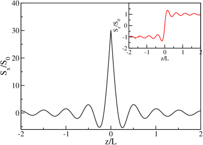
The and indices naturally refer to electrons incident from the left and right, which are held at a potential drop of symmetrically across the Fermi energy . is the density of states of the carriers. In the region around the DW the transpose component of the spin density is enhanced, see Fig. 1. Density fluctuations are also clearly visible.
The uncoupled Green’s function in the scattering basis becomes
| (11) |
using the shorthand
| (12) |
with the dispersion of the incoming electrons’ . The chemical potential will also depend on the scattering state as the electrons incoming from the left/right have a different chemical potential: , respectively.
Ultimately we are interested in the current through the system:
| (13) |
for spin electrons. We are interested in the steady state case where there is no charge build up in the wire. The current is then
| (14) |
We can substitute in our perturbative expression Eq. (9), and Eq. (11) and work in the limit of zero temperature.
IV Results
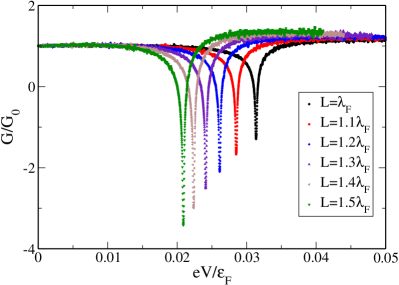
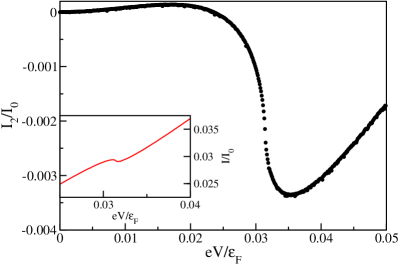
The results are plotted in Figs. 2 and 3, the negative differential conductance is marked by a dip in the current around the lowest resonance . We consider magnetic semiconductor wires Rüster et al. (2003); Sugawara et al. (2008); Matsukura (1998) where the DW width can be closer to the Fermi wavelength, the width of the wall can be atomically sharp when constrictions are present Bruno (1999); Pietzsch et al. (2000); Ebels et al. (2000). Hence we take , . The mode energy is , where is the cross section and is the lattice spacing. To keep this energy within experimentally reasonable sizes, we consider quasi-one-dimensional wires where . This gives us Thiele (1973), and for the unrenormalized coupling we take
At low temperatures in such systems electron-correlation effects tend to renormalize the coupling strengths.Araújo et al. (2006); Sedlmayr et al. (2011c) Hence we take the effective coupling as , with and . The scattering strengths from the DW will be similarly renormalized.
Of experimental relevance is the differential conductance which can be defined as . This is plotted in Fig. 2 for different DW widths, and the negative differential conductance occurs around the resonant energy level . Higher modes of the DW’s motion would couple similarly at different energies for larger applied bias.
We note that the model developed in this work is also relevant to interacting quantum dot systems involving regions with a noncollinear magnetization.Sedlmayr et al. (2006); Sedlmayr and Berakdar (2008) This is the subject of ongoing work.
With regard to an experimental realization we note the following: NDMR is sizable for DWs in magnetic-semiconductor-based nanowires such as those realized in Refs. Rüster et al., 2003; Sugawara et al., 2008; Matsukura, 1998. We developed the above theory however for electrons as carriers whereas in III-V compounds the carriers are holes. As follows from the above treatment, the underlying mechanisms for the emergence of NDMR are however the DW scattering and inferences of the carriers coupled to the modes of the DW. These elements will also be present for carrier holes despite their more complicated electronic dispersion, and hence we expect NDMR to also be present in this case.
V Summary
In summary, we have calculated the current through a ferromagnetic wire with a domain wall present, or equivalently a thin ferromagnetic strip between ferromagnetic wires of opposing magnetization. Particular attention has been paid to the effects of the lowest modes of the DWs motion caused by the presence of this current. In order to solve for the density build up around the domain wall subject to an applied potential we used a soluble model for a sharp DW. The negative differential magnetoresistance expected from the excitation of these modes by the current electrons is clearly visible in the differential conductance depicted in Fig. 2. This qualitatively new effect offers new opportunities for applications in spintronics and domain wall logics Allwood et al. (2005) similar to those that utilize NDR in charge-based electronics.
Acknowledgments
We thank V. Dugaev for many valuable discussions. This work is supported by the DFG contract BE 2161/5-1, and SFB 762, and by the Graduate School of MAINZ (MATCOR).
References
- Lifschitz and Pitaevskii (2002) E. M. Lifschitz and L. P. Pitaevskii, Statistical Physics Part 2: Theory of the Condensed State (Butterworth-Heinemann, 2002).
- Gilbert (2004) T. L. Gilbert, IEEE Transactions on Magnetics 40, 3443 (2004).
- Zhang and Li (2004) S. Zhang and Z. Li, Phys. Rev. Lett. 93, 127204 (2004).
- Slonczewski (1996) J. C. Slonczewski, Journal of Magnetism and Magnetic Materials 159, L1 (1996).
- Marrows (2005) C. H. Marrows, Advances in Physics 54, 585 (2005).
- Parkin et al. (2008) S. Parkin, M. Hayashi, and L. Thomas, Science 320, 190 (2008).
- Sedlmayr et al. (2009) N. Sedlmayr, V. K. Dugaev, and J. Berakdar, Phys. Rev. B 79, 174422 (2009).
- Sedlmayr et al. (2011a) N. Sedlmayr, V. K. Dugaev, and J. Berakdar, Phys. Rev. B 83, 174447 (2011a).
- Sedlmayr et al. (2011b) N. Sedlmayr, V. K. Dugaev, M. Inglot, and J. Berakdar, physica status solidi (RRL) Rapid Research Letters 5, 450 (2011b).
- Dugaev et al. (2006) V. K. Dugaev, J. Berakdar, and J. Barnaś, Phys. Rev. Lett. 96, 047208 (2006).
- Winter (1961) J. M. Winter, Phys. Rev. 124, 452 (1961).
- Thiele (1973) A. A. Thiele, Phys. Rev. B 7, 391 (1973).
- Rebei and Mryasov (2006) A. Rebei and O. Mryasov, Phys. Rev. B 74, 014412 (2006).
- Kiselev et al. (2003) S. I. Kiselev, J. C. Sankey, I. N. Krivorotov, N. C. Emley, R. J. Schoelkopf, R. A. Buhrman, and D. C. Ralph, Nature 425, 380 (2003).
- Saitoh et al. (2004) E. Saitoh, H. Miyajimi, T. Yamaoka, and G. Tatara, Nature 432, 203 (2004).
- Balkan et al. (1993) N. Balkan, B. K. Ridley, and E. A. J. Vickers, Negative Differential Resistance and Instabilities in 2-D Semiconductors (Springer, Heidelberg, 1993).
- Chang et al. (1974) L. L. Chang, L. Esaki, and R. Tsu, Applied Physics Letters (1974).
- Wei et al. (2006) J. H. Wei, S. J. Xie, L. M. Mei, J. Berakdar, and Y. Yan, New Journal of Physics 8, 82 (2006).
- Wei et al. (2007) J. H. Wei, S. J. Xie, L. M. Mei, J. Berakdar, and Y. Yan, Organic Electronics 8, 487 (2007).
- Trocha et al. (2009) P. Trocha, I. Weymann, and J. Barnaś, Phys. Rev. B 80, 165333 (2009).
- Matthaei (1964) G. L. Matthaei, Microwave Filters, Impedance-Matching Networks, and Coupling Structures (McGraw-Hill, New York, 1964).
- Chattopadhyay and Rakshit (2006) D. Chattopadhyay and P. Rakshit, Electronics: fundamentals And Applications (New Age International, 2006).
- Willardson and (Eds.) R. K. Willardson and A. C. Beer (Eds.), Semiconductors and Semimetals: Applications and devices (Academic Press, New York, 1971).
- Allwood et al. (2005) D. A. Allwood, G. Xiong, C. C. Faulkner, D. Atkinson, D. Petit, and R. P. Cowburn, Science 309, 1688 (2005).
- Wickles and Belzig (2009) C. Wickles and W. Belzig, Phys. Rev. B 80, 104435 (2009).
- Levy and Zhang (1997) P. M. Levy and S. Zhang, Phys. Rev. Lett. 79, 5110 (1997).
- Dugaev et al. (2002) V. K. Dugaev, J. Barnaś, A. Łusakowski, and L. A. Turski, Phys. Rev. B 65, 224419 (2002).
- Tatara and Fukuyama (1997) G. Tatara and H. Fukuyama, Phys. Rev. Lett. 78, 3773 (1997).
- Araújo et al. (2006) M. Araújo, V. K. Dugaev, V. Vieira, J. Berakdar, and J. Barnaś, Phys. Rev. B 74, 224429 (2006).
- Sedlmayr et al. (2006) N. Sedlmayr, I. V. Yurkevich, and I. V. Lerner, EPL (Europhysics Letters) 76, 109 (2006).
- Rammer and Smith (1986) J. Rammer and H. Smith, Rev. Mod. Phys. 58, 323 (1986).
- Kamenev (2005) A. Kamenev, Nanophysics: Coherence and Transport (Elsevier, Amsterdam, 2005), p. 177.
- Dugaev et al. (2003) V. K. Dugaev, J. Berakdar, and J. Barnaś, Phys. Rev. B 68, 104434 (2003).
- Rüster et al. (2003) C. Rüster, T. Borzenko, C. Gould, G. Schmidt, L. Molenkamp, X. Liu, T. Wojtowicz, J. Furdyna, Z. Yu, and M. Flatté, Phys. Rev. Lett. 91, 216602 (2003).
- Sugawara et al. (2008) A. Sugawara, H. Kasai, A. Tonomura, P. Brown, R. Campion, K. Edmonds, B. Gallagher, J. Zeman, and T. Jungwirth, Phys. Rev. Lett. 100, 0477202 (2008).
- Matsukura (1998) F. Matsukura, Phys. Rev. B 57, R203 (1998).
- Bruno (1999) P. Bruno, Phys. Rev. Lett. 83, 2425 (1999).
- Pietzsch et al. (2000) O. Pietzsch, A. Kubetzka, M. Bode, and R. Wiesendanger, Phys. Rev. Lett. 84, 5212 (2000).
- Ebels et al. (2000) U. Ebels, A. Radulescu, Y. Henry, L. Piraux, , and K. Ounadjela, Phys. Rev. Lett. 84, 983 (2000).
- Sedlmayr et al. (2011c) N. Sedlmayr, S. Eggert, and J. Sirker, Phys. Rev. B 84, 024424 (2011c).
- Sedlmayr and Berakdar (2008) N. Sedlmayr and J. Berakdar, EPL (Europhysics Letters) 83, 57003 (2008).