Signal and noise of Diamond Pixel Detectors at High Radiation Fluences
Abstract
CVD diamond is an attractive material option for LHC vertex detectors mainly because of its strong radiation-hardness causal to its large band gap and strong lattice. In particular, pixel detectors operating close to the interaction point profit from tiny leakage currents and small pixel capacitances of diamond resulting in low noise figures when compared to silicon. On the other hand, the charge signal from traversing high energy particles is smaller in diamond than in silicon by a factor of about 2.2. Therefore, a quantitative determination of the signal-to-noise ratio (S/N) of diamond in comparison with silicon at fluences in excess of 1015 neq cm-2, which are expected for the LHC upgrade, is important. Based on measurements of irradiated diamond sensors and the FE-I4 pixel readout chip design and performance, we determine the signal and the noise of diamond pixel detectors irradiated with high particle fluences. To characterize the effect of the radiation damage on the materials and the signal decrease, the change of the mean free path of the charge carriers is determined as a function of irradiation fluence. We make use of the FE-I4 pixel chip developed for ATLAS upgrades to realistically estimate the expected noise figures: the expected leakage current at a given fluence is taken from calibrated calculations and the pixel capacitance is measured using a purposely developed chip (PixCap). We compare the resulting S/N figures with those for planar silicon pixel detectors using published charge loss measurements and the same extrapolation methods as for diamond. It is shown that the expected S/N of a diamond pixel detector with pixel pitches typical for LHC, exceeds that of planar silicon pixels at fluences beyond 1015 particles cm-2, the exact value only depending on the maximum operation voltage assumed for irradiated silicon pixel detectors.
keywords:
Detector physics, Solid state detectors, Hybrid detectors, Radiation-hard detectors, Pixel detectors, Radiation damage to solid state detectors1 Introduction
After almost three decades of successful operation of gaseous or silicon microstrip vertex detectors at most high energy physics collider experiments, the LHC detectors ATLAS [1], CMS [2], and ALICE [3] have for the first time installed large silicon pixel detectors [4, 5, 6] as their innermost detection elements for precision tracking and vertexing close to the collision point. Pixel detectors are capable of coping with the large data rates at the LHC and can survive the large radiation fluences in the vicinity close to the collision point. Since the start of the LHC in 2009 they have proven to be precise and reliable detection devices [7, 8, 9, 10, 11]. In the context of the LHC upgrade program [12], in particular the expected increase in luminosity by up to a factor 10 compared to the present LHC design [13] and the corresponding increase in particle rates and radiation levels, strong constraints on detector layouts and materials are imposed. While steady progress in microelectronics helps to cope with the resulting data rates, new sensor solutions must be targeted to withstand particle fluences in excess of 1016 cm-2 absorbed over the machine’s lifetime.
In attempting to cope with this fierce radiation environment, sensor materials with a strong intrinsic radiation resistance come to mind. In this category diamond, grown by chemical vapor deposition (CVD), is a candidate due to its large band gap of 5.5 eV and its strong lattice, for which a minimum displacement energy of 43 eV [14] is needed to kick-off an atom from the lattice (25 eV in Si [15]). CVD diamond detectors are produced as poly-crystalline (pCVD) and single-crystal (scCVD) detectors. The large band gap also results in quasi negligible leakage current, an important noise factor. Moreover, the pixel capacitance should be significantly smaller for diamond than for silicon pixels, not only because of the smaller dielectric constant (= 5.7; = 11.9) but also because of the more complex structure of implants and guard rings in the case of silicon [16]. On the negative side, also due to the larger band gap, the average energy required to liberate an e/h-pair in diamond is 13.1 eV, 3.6 times larger than for silicon, resulting in a smaller signal, at least before irradiation. To assess whether this still holds true after heavy irradiation, the development of signal and signal-to-noise (SNR) as a function of radiation fluence is determined in this paper. As a model pixel system we adopt the current ATLAS pixel modules developed for the insertable B-layer project, IBL [17] with silicon pixel sensors and its diamond beam monitor companion (DBM). Both are equipped with the pixel readout chip FE-I4 [18, 19].
First, we describe the signal and its development with increasing particle fluence. The damage is characterized in terms of the mean free path of the charge carriers:
| (1) |
where ve/h and are the velocities and lifetimes of the charge carriers.
Then we determine the expected noise using the ATLAS pixel readout chip FE-I4 [18, 19] as a reference for calculations and simulations. Two important noise parameters, the leakage current (ileak) and the input capacitance coupled to the preamplifier (CD), are either calculated or measured, respectively. Finally, the SNR as a function of fluence is determined from these ingredients. In these steps we keep the corresponding results for planar silicon pixel sensors [16] operated with the same readout chip and biased with voltages up to 600 V as a reference.
2 Diamond sensor characterization
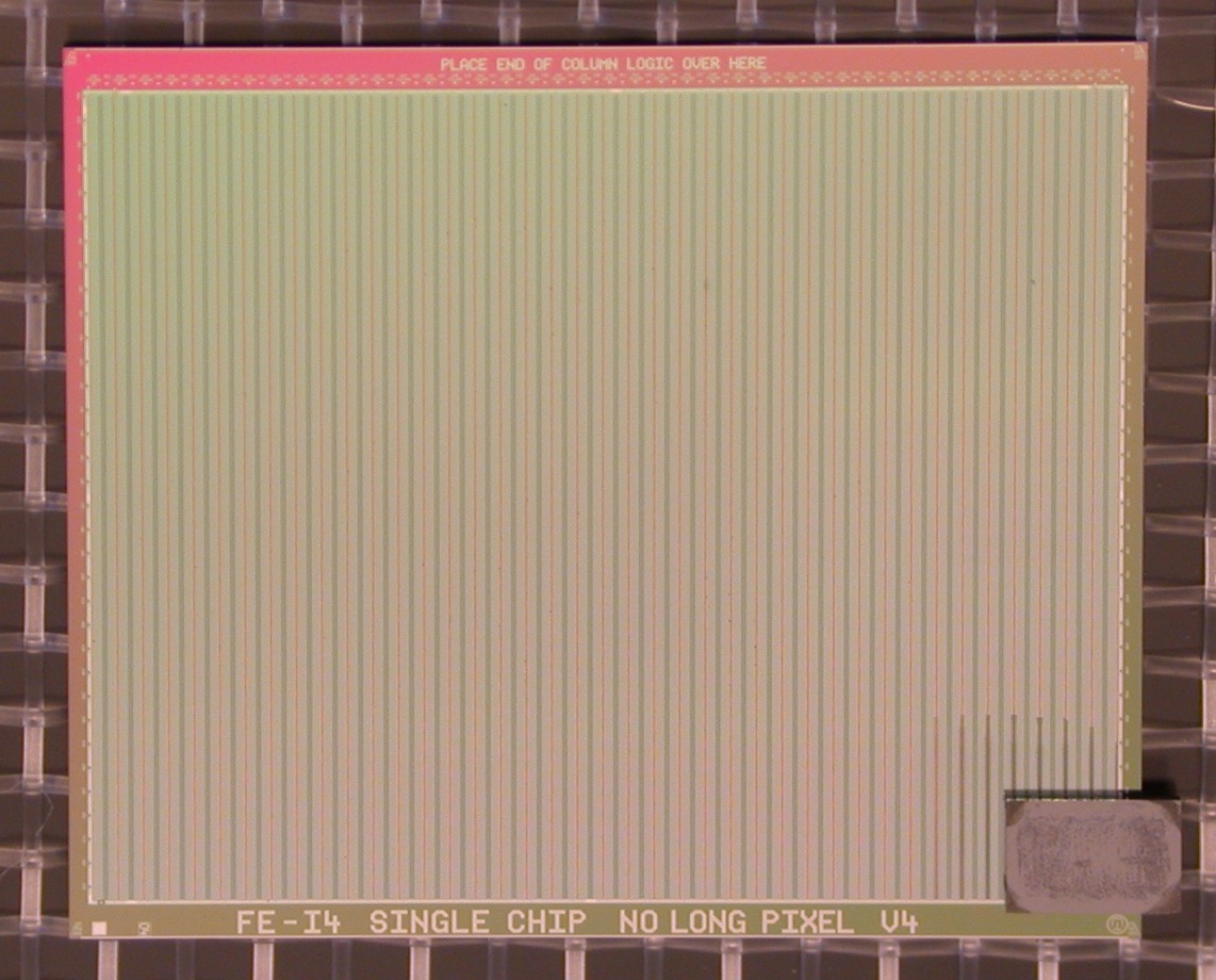
We evaluate the signal to noise of diamond pixel sensors that are bonded to the ATLAS pixel readout chip FE-I4 [19]. This chip is the successor of the FE-I3 chip [20] currently installed in ATLAS, and has been developed to cope with the demands of the next generation of pixel detectors. The FE-I4 chip has been bonded to different sensor types, among them planar [16] and 3D-silicon [21] sensors as well as diamond sensors [22]. The area of one pixel is 50 250 m, and the entire chip has 26880 pixels in 80 columns and 336 rows. The FE-I4 will serve as the base readout chip for the pixel detector upgrade developments in the coming years and is this particularly suited for this study.
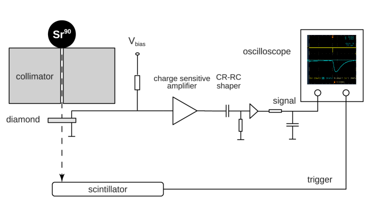
The measurement of the change in signal charge before and after irradiation should not depend on the type of readout used and is thus performed using detectors equipped with a single channel charge sensitive readout connected to a readout pad on the diamond sensor. Because the effects of radiation damage differ largely for different energies, the scCVD and pCVD diamond pad detectors have been irradiated with 24 GeV protons at the CERN SPS [23] and with 25 MeV protons at the Karlsruhe Synchrotron [24] to various fluences. Their charge signal has been measured before and after the irradiation to assess the relative signal loss. The measurement is done with the setup shown in Fig. 1. A 90Sr -source with a 2.28 MeV endpoint energy is used. In order to select only straight, high energetic tracks of the 90Sr spectrum that closely represent the energy deposit of a minimum ionizing particle, electrons need to pass a collimator and reach a scintillator for triggering. Range calculations show that with the given material the electrons must have a minimum energy of about 1.05 MeV corresponding to to trigger and are thus considered very close to minimum ionizing [25]. Hardening the -spectrum by adding additional material sheets into the electron’s flight path between sensor and scintillator did not change the measured average signal. The charge deposited by the triggered electrons in the sensor is read out by a charge sensitive preamplifier [26] and a pulse shaper system[27] with a 2.5 s shaping time. The analysis of the data is shown in section 3.2.
3 The signal
3.1 Energy deposit and charge signal
The absolute signal charge is calculated from the energy deposit in the sensor and the average energy needed to create an electron/hole pair (see section 1). The energy released per cm in the diamond or silicon sensors is given in [25] including the effects of -electrons leaving the sensor. The most probable value is calculated following [25]
| (2) |
where MeV, for a detector with a thickness of x g cm-2; parametrizes the density effect on the energy loss and is the average ionization energy. The respective values for diamond and silicon are given in Table 1.
| parameter | diamond | Si |
|---|---|---|
| I | 81 eV | 174 eV |
| 1.84 | 0.95 | |
| 13.1 eV | 3.61 eV |
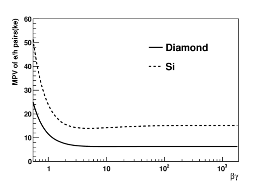
The energy deposit in diamond per unit thickness is larger than in silicon mainly due to the larger density (see Fig. 2). The ratio for a 1 GeV incident pion ( = 7.2) is
| (3) |
The signal charge released for a given deposited energy is obtained by dividing the energy deposition (MPV) by the energy required to generate an e/h-pair (Table 1). For a 200m thick sensor, this yields about 14 000 (Si) and 6 300 (diamond) e/h-pairs, respectively for 1 GeV pions before irradiation.
3.2 Radiation damage and signal losses
If the mean free path of the charge carriers is much larger than the thickness of the sensor, the signal measured by a charge sensitive amplifier corresponds to the collection of the entire generated charge. Heavy irradiation introduces trapping centers into the sensor crystal which in turn reduces . Especially in silicon, additional effects like the change of the effective doping concentration as well as increased leakage current generation also occur, which are treated in section 4.
Radiation effects in diamond
In former studies of diamond sensors [30, 31], the signal loss in diamond due to irradiation has been characterized by the charge collection distance CCD which is defined as the ratio of the measured collected charge and the charge generated by ionization multiplied by the detector thickness:
| (4) |
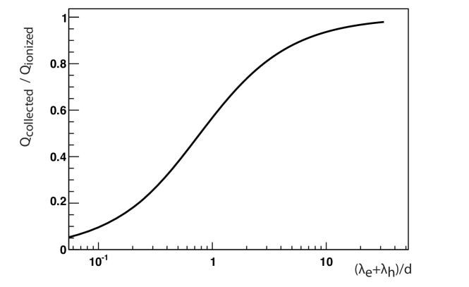
The charge collection distance ceases to be a good characterization quantity when is larger than the sensor thickness which is generally the case for unirradiated silicon but also for present day single crystal diamond sensors [32]. In general, itself is the appropriate quantity to characterize the signal loss. It relates to CCD as [33]:
| (5) |
The relation is displayed in Fig. 3. For large , CCD reaches . For CCD and are about the same.
Radiation effects in silicon
While for diamond the effect of strong irradiation causes a loss of signal charge due to trapping and a reduction of , for silicon additional effects must be taken into account. Radiation damage effect to silicon have been studied intensively and are reliably described by the so called NIEL hypothesis [34] , according to which all damage can be traced to point and cluster defects created by non-ionizing energy loss in the lattice. With increasing radiation the effective doping concentration changes leading to a smaller depletion depth at the same bias voltage. At very high fluences, and with high electric fields inside the sensor, charge multiplication effects have been reported [35]. Finally, also the geometry of the pixel electrodes plays an important role. Conventional sensors with planar pixel electrodes require high operating voltages after irradiation, and cannot be fully depleted. In contrast, 3D-silicon pixels [21] remain fully depleted even at moderate bias voltages. While these effects influence the signal, the noise is dominated by the increase in leakage current due to irradiation, common to both planar and 3D pixel sensors. 3D sensors also have more capacitance than planar sensors (see section 4.3).
Comparison of diamond with silicon
These various facts render a direct comparison of diamond with silicon signals difficult. We have thus chosen to compare our measurements obtained using diamond sensors with published silicon data [35, 36] for about the same electric field strength (1.8-2.2 V/m) before irradiation. This corresponds to 900 V on 500 m thick diamond sensors and 600 V for 310 m thick silicon sensors when operated in over-depletion [35, 36].
At LHC, a mixture of particles with a broad energy spectrum damages the detectors and electronics with energy and particle type dependent damage effects. Low energy (MeV) particles create larger damage than high energy (GeV) ones. Irradiations of scCVD and pCVD diamond sensors have been performed by the RD42 collaboration [22] for protons and neutrons at various energies between 25 MeV and 24 GeV. In the absence of a generally accepted NIEL damage normalization for diamond, e.g. to 1 MeV neutron damage, we refer in this paper to these two energies for proton damage because (a) they have been characterized by ourselves and (b) they correspond well to the high and low energy parts of the particle energy spectrum at the LHC. For silicon we use published data of irradiated Si planar n-in-p FZ pixel sensors [35, 36]. The sensors have a thickness of 310m and are read out by strip electrodes with 80m pitch. The measurements were performed with a bias voltage of 500 V and 700 V, respectively, and have been averaged for an assumed bias voltage of 600 V.
is obtained by using eq. (5), where the collected charge is by measurement (diamond) or from publication (Si), and the generated charge is calculated from eq. (LABEL:eq:bethe).
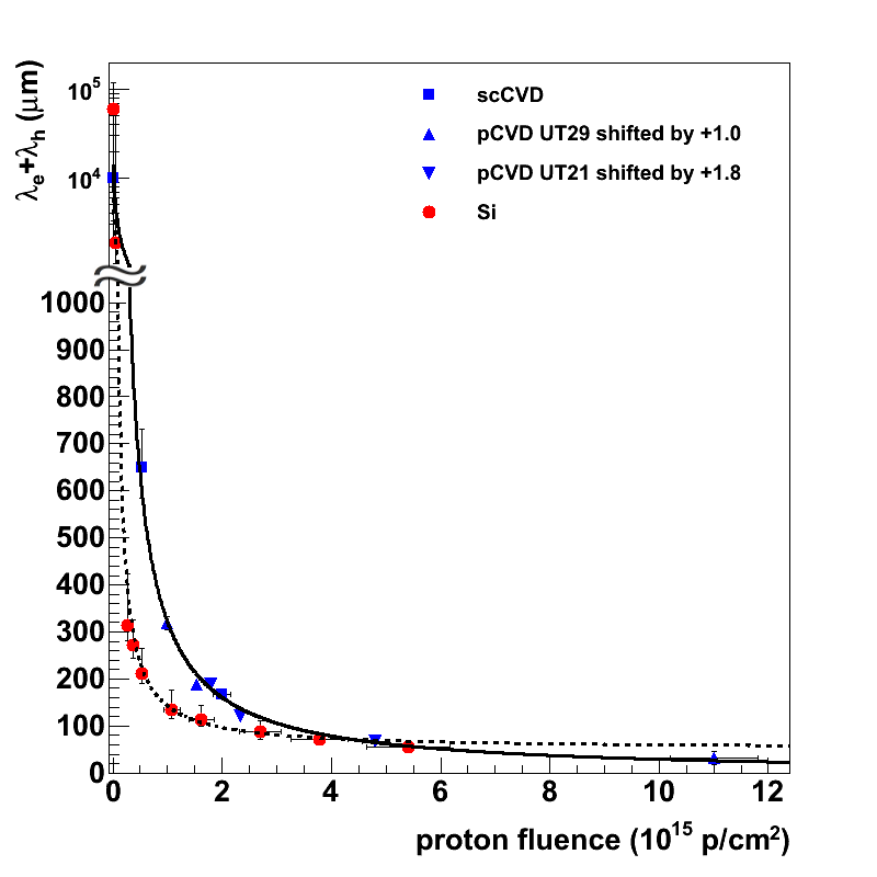
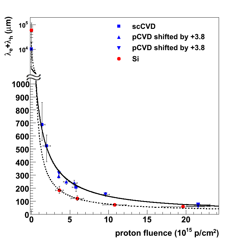
Figure 4 shows damage curves measured for irradiations with 25 MeV and 24 GeV protons, respectively. Displayed is as a function of the radiation fluence. The shape of the damage curves generally follows the parametrization [33]:
| (6) |
where is the fluence and is the mean free path before irradiation. is the damage constant parametrizing the material’s irradiation hardness. Fig. 4 contains data for diamond in mono-crystalline (single crystal, scCVD) and poly-crystalline (pCVD) form. Note that the pCVD diamond damage curves follow the same shape as the scCVD, but must be shifted to the right by a sample-dependent amount to fit the same curve. This means that their initial mean free path is shorter than that of the scCVD sample, because their less homogeneous substrate volume contains grain structures leading to a larger trapping center density [37]. Note however, that the shift is comparatively small once fluences above 1015 cm-2 have been reached. A fit to the functional form of eq. (6) is performed to extract the damage constant . In this the pCVD data shift value is determined yielding minimal overall .
For silicon sensors damaged from radiation fluences above 1015 neq cm-2 and operated at high bias voltages, charge multiplication effects have been reported [35]. As a consequence, the silicon data in Fig. 4 do not follow the functional form of eq. 6. In order to account for possible charge multiplication effects the parametrization of eq. 6 has been changed by an additional term:
| (7) |
The corresponding fits yield for all diamond and Si data and m and m for silicon damaged by 25 MeV and 24 GeV protons, respectively. This supports the observation of an onset of charge multiplication in the low energy radiation data (25 MeV) which is more damaging than the high energy radiation data. For the 24 GeV Si data is consistent with zero within errors, whereas for the diamond data is found negligible. Table 2 shows the results. The damage constant for diamond is generally smaller than for Si by a factor of 2 - 3.
| 25 MeV protons | 24 GeV protons | |
|---|---|---|
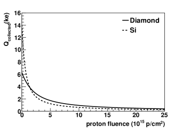
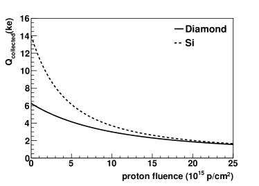
With the damage constants , eq. (6), and relation (5) we can determine the signal charge at any fluence value for a given sensor thickness. For a minimum ionizing particle ( = 100) and for 200 m thick sensors the signal charge (without charge multiplication) is plotted in Fig. 5 as a function of the fluence.
4 The Noise
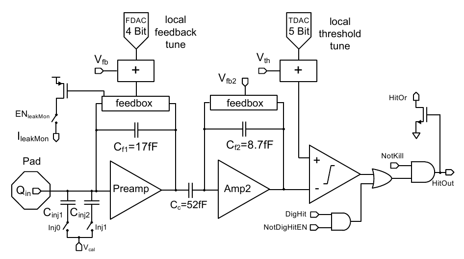
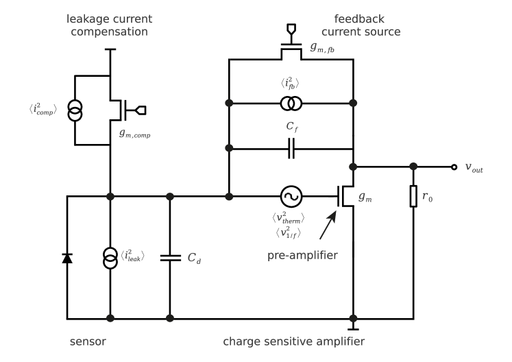
The FE-I4 chip [18, 19] is a two-stage charge sensitive amplifier featuring constant current feedback in both stages followed by a discrimination stage. The two amplifier stages are capacitively coupled. A leakage current compensation circuit is implemented at the input to compensate sensor leakage current up to 100 nA. The chip has been optimized for a maximum input capacitance of 400 fF. Figure 6 shows a block diagram of the FE-I4 cell circuitry.
For the noise estimate of a pixel sensor - readout chip configuration we employ (a) a calculation using a noise model assuming some simplifications detailed below and (b) detailed noise simulations on the original FE-I4 chip layout using the Virtuoso SPECTRE Circuit Simulator simulation package in CADENCE [38].
4.1 Calculation of FE-I4 noise
For the noise calculation the contributions of the second stage of the FE-I4 amplifier have been neglected and only the dominant noise sources shown in Fig. 7 have been considered: thermal and 1/f-noise in the transistor channel which appear as series voltage noise at the input of the preamplifier; shot noise from the sensor leakage current and thermal noise from the leakage current compensation transistor, as well as thermal noise in the feedback loop (see Fig. 7) which constitute a parallel noise contribution.
The noise sources mentioned above generate a noise voltage at the output of the amplifier. Integrating the total noise power spectral density multiplied by the amplifier transfer function we obtain the following formula for the equivalent noise charge:
| (8) | |||||
| (9) | |||||
| (10) | |||||
| (11) |
Here , , are time constants. The drain output conductance of the feedback transistor is feedback current dependent. A typical value for for signals just above threshold is 4.5 nA and nS. is the feedback capacitance of the first stage CSA. is the leakage current. = 225 is the transconductance of the preamplifier input transistor. The FE-I4 nominal bias current is 7.5A. J is the 1/f noise coefficient. , , and are the oxide capacitance, width, and gate length of the MOSFET transistor.
Note that the noise performance depends to a large extent on the detector leakage current () and the value of the input capacitances to the preamplifier , both of which need to be determined. The detector leakage current, , is obtained for a given fluence as described by eq. (12) below. The precise values of pixel sensor capacitances are a priori not well known and have always been an uncertainty in the characterization of pixel performance. We therefore have measured as described in section 4.3 using a dedicated capacitance measurement chip.
While diamond - owing to its large band gap - can be assumed to have negligible leakage current even after strong irradiation, the leakage current change in silicon due to irradiation follows the relation (NIEL approximation) [34]:
| (12) |
where V is the volume under the pixel electrode, is the damage factor for silicon ( [34]) and hence can be calculated. The predicted NIEL linear behavior has been verified for silicon by measurements up to fluences of 10/cm2 [39]. Even if assumed to be zero before irradiation, can become fairly large ( (100 nA)) at large fluences in excess of 10/cm2 as expected at the LHC-upgrades. Furthermore, a temperature correction has been applied, because the typical operation temperature () at LHC is -10∘C while the measurements reported here have been done at room temperature ():
| (13) |
where is the band gap of Si, and is the Boltzmann constant.
4.2 Noise simulation
The noise of the FE-I4 based pixel detector was also determined by simulations of the analog part of the FE-I4 using the Virtuoso Spectre Circuit Simulator [38].
AC noise simulation is a common approach for small signal noise analysis which employs a linearized model of the circuit at its DC operating point. The noise is simulated in the frequency domain, treating the signal and noise sources separately assuming that they do not influence each other.
The transient noise simulation is performed in the time domain. It is better suited than the AC simulation for our noise studies which evaluate the noise by S-curve measurements using multiple charge injections. Fluctuations of the signal peak when reaching the applied threshold voltage are of interest. In this case the operation point is far away from its stable DC value and hence the accuracy of the AC simulation is limited. In the transient noise simulation, each component of the electronic circuit contains a noise source generating random noise signals in the time domain with the appropriate power spectral density distribution. The circuit voltages and currents are computed solving differential equations by effective Monte Carlo methods. This method allows fairly realistic noise studies of non-linear and non-time invariant systems. In the simulation, a noise frequency band from 10 kHz to 1 GHz was chosen to extend well beyond the circuit bandwidth.
In Fig. 8 we show the dependence of the noise calculations and simulations as a function of the most important parameters in this estimate, and . For Fig. 8(a) has been assumed. For Fig. 8(b) pixel capacitances of fF have been assumed for silicon, while for diamond is assumed (see section 4.3). Noise measurements obtained with (a) unirradiated devices for diamond and silicon and (b) with silicon pixel assemblies irradiated to a fluence of 1015 neq/cm-2 corresponding to (eq. 12) are included in Fig. 8 to verify the noise predictions. The agreement is remarkably good.
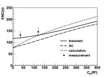
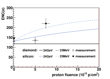
Given that the calculation and the transient noise simulation agree at the 5- and 20-level, and also agree reasonably well with measurements of the noise, we assume the transient noise model for the following SNR estimations.
4.3 Measurement of and
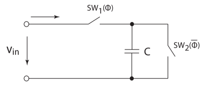
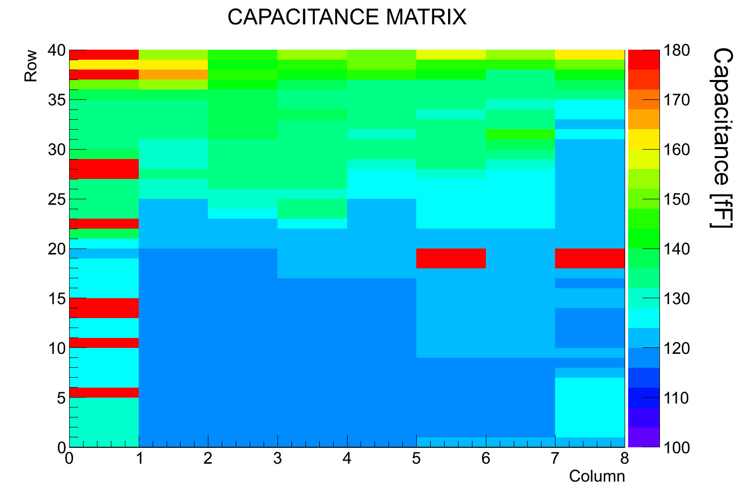
The knowledge of the total input capacitance coupled to the preamplifier is an important ingredient for a reliable comparison between diamond and silicon. It receives contributions from the sensor’s interpixel capacitance (dominant), its capacitance to the backside, the capacitances of the solder bump and the bump pad, as well as the amplifier input capacitance. While in the case of diamond the interpixel capacitance is geometrically defined by the pixel metallization, for silicon the pixel implant geometry and the (punch through) biasing grid geometry define the pixel capacitance. Thus a simple scaling with the dielectric constants of both materials is not expected. In order to obtain reliable values of for diamond and silicon pixels with FE-I4 pixel sizes and pitch, we have developed a capacitance measurement chip (PixCap) [40] for the measurement of the capacitance with high accuracy. The chip has been bonded to the pixel sensors using the bump and flip-chip technology.
The measurement principle is based on a switching circuit (Fig. 9(a)) that charges and discharges the capacitance to be measured with a chosen frequency . By measuring the average switching current at a well determined frequency and input voltage the capacitance is extracted:
| (14) |
where is the input voltage and the switching frequency (here 4 MHz). Leakage current is corrected for by dedicated measurements [40].
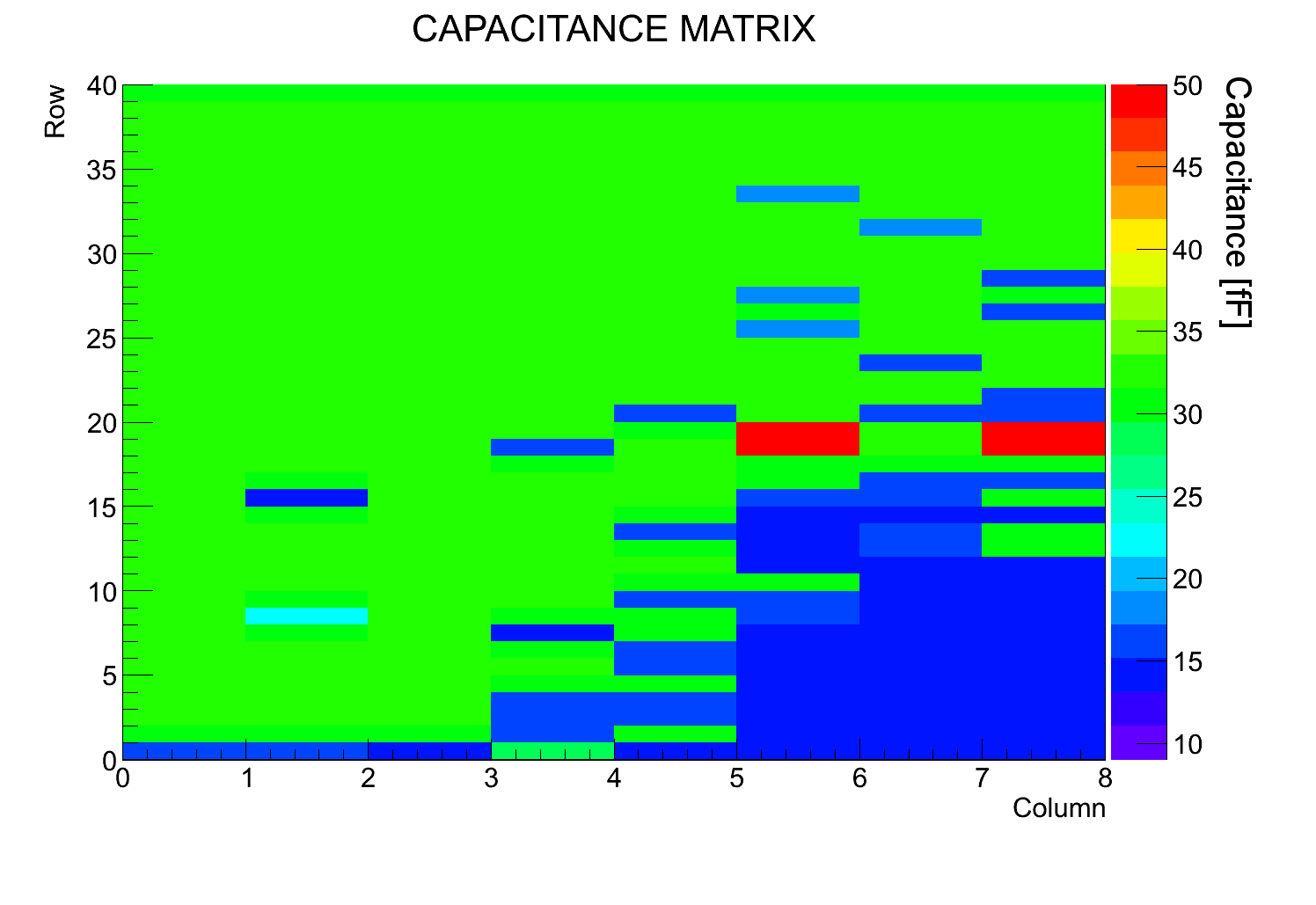
By individually programming the switching sequences for neighboring pixels the different contributions to the total capacitance can be individually determined. The measurement error depends on the leakage current and the capacitance value and lies around 0.1 fF for diamond and 0.3 fF for silicon. The capacitance measurements yield the following results. Without any sensor bonded, the input capacitance to the FE-I4 preamplifier is . The capacitance of the input transistor transistor itself is . Bonded to a diamond sensor the map of measured pixel capacitances is shown in Fig. 10(a). The sensor was biased with 60V, although no dependence of the bias voltage is observed. The average pixel capacitance measured for diamond bumped to the FE-I4 cell, i.e. including all related connection capacitances but without the transistor capacitance is measured to be
where the error includes the spread over the considered region of the pixel matrix (see Fig. 10). For silicon there is a dependence on the applied bias voltage until the sensor is fully depleted and neighboring pixels are isolated. For unirradiated sensors this is the case for voltages above 60 V. The measured capacitance map is shown in Fig. 10(b). The average value for silicon is
5 Signal to noise ratio at high particle fluence
With the measured capacitances and the fluence dependent leakage current calculations, it is now possible to predict the noise as a function of the fluence for a given energy of the damaging radiation. In order to compare diamond in a reasonable way with silicon sensors some assumptions (for silicon) have to be made:
-
-
The electrode geometry changes the characteristics of a silicon pixel detector. Currently only two viable options exist, sensors with planar pixel electrodes on one side of the sensor [16] and sensors with cylindrical electrodes etched into the silicon bulk, so called 3D-Si-sensors [21]. We chose here to base our comparison with diamond on planar pixel sensors mated to the identical FE-I4 pixel chip.
-
-
In contrast to diamond, silicon needs to be made free of charge carriers by depletion. For increasing irradiation the voltage which is needed for full depletion of a Si-sensor needs to be increased. This will be possible only to a certain maximal extent in a large area pixel detector system and will be limited by the power that can be afforded. At fluences much above 1015 neq cm-2, a 200 m thick Si-sensor can usually no longer be fully depleted, and the depletion depth will change with increasing irradiation even if the bias voltage is steadily increased.
We hence base our comparison on irradiation measurements made by Affolder et al. [35, 36] for 310 m thick silicon sensors and assume that the maximum bias voltage to be 600 V111Valuesfor this bias setting have been obtained by averaging the measurements quoted in ref. [35, 36] for 500 V and 700 V which corresponds to the current power supply limit in ATLAS.
-
-
In thin silicon sensors irradiated to fluences up to 5.6 1015 neq cm-2, charge multiplication has been observed [41]. We ignore this possibility for this study, because it has not been demonstrated yet whether charge multiplication can be exploited for a (homogeneous) operation of pixel detectors for particle detection after large fluences. It is also possible that similar effects can occur in diamond detectors in high electric fields.
We conclude therefore, that our assessment of diamond pixels compared to planar Si-pixel detector assemblies, both bonded to the FE-I4 pixel readout chip, constitutes a reasonable and fair choice for a comparison, notwithstanding the possibility that different operation points and designs may partly impart our conclusions.
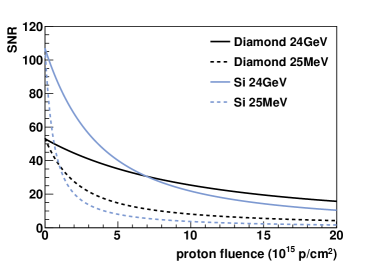
With the measured signal development as a function of fluence from section 3 we plot the signal-to-noise ratio (SNR) for an assumed pixel sensor thickness of 200 m and for the two different damage energies in Fig. 11(a). While the different responses to high and low energy irradiation lead to different SNR predictions the conclusion of Fig. 11(a) is nevertheless evident: diamond pixel modules exceed the performance of (planar) Si pixels in terms of the SNR at fluences above , for scCVD between about (25 MeV protons) and (24 GeV protons). For pCVD diamond this cross over point would be shifted to the right by p/cm2 (24 GeV protons) and by p/cm2 (25 MeV protons, see Fig. 4).
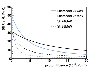
Since the question of how much material a pixel vertex detector or tracker constitutes is important in design considerations for large collider detectors, a fair comparison should also account for this effect. Fig. 11(b) therefore shows the same dependence as Fig. 11(a), but for sensors of the same thickness in terms of radiation length: 0.1 X0. This normalization moves the turn-over point in the diamond - silicon comparison to lower values of the radiation fluence, namely to about p cm-2 (25 MeV protons) and p cm-2 (24 GeV protons), respectively. This comparison does not take into account that cooling and other services also play an important role in the material budget, in particular for silicon sensors which at HL-LHC require operation temperatures well below 0o C [4, 5].
6 Conclusions
This paper presents an assessment of the performance of diamond pixel detectors relative to silicon pixels at very high radiation fluences quantified in terms of the signal-to-noise ratio (SNR). For the study pixel detector assemblies (single chip modules) based on the ATLAS pixel readout chip FE-I4 have been used, both for diamond and for Si. The individual ingredients to this quantity are each determined whenever possible by measurements, aided by calculations/simulations as a function of fluence. The signal development with fluence is extracted from dedicated irradiation campaigns up to fluences of 1016 p/cm2 at two different energies, 25 MeV and 24 GeV protons, as well as from published data on silicon [35, 36]. In order to properly treat the two materials with a large mobility-lifetime product, the mean free path rather than the charge collection distance has been employed. The damage constants determined from a fit to the damage curves are 2 - 3 times smaller for diamond than they are for silicon. Poly-crystalline diamond differs from mono-crystalline one in this by a shift of the damage curves to lower fluences by an amount of between 1 to 3.8 x 10¹⁵ p/cm, depending on the irradiation energy. For the noise determination the actual layout of the FE-I4 pixel chip has been used in a transient noise simulation, backed by an analytical calculation. The two most important parameters in the noise determinations, the leakage current and the pixel input capacitance to the preamplifier , have been either derived () as a function of fluence using the NIEL assumption, or measured () using a dedicated capacitance measurement chip (PixCap [40]). The resulting SNR leads to the conclusion that the SNR of diamond pixel sensors exceeds that of planar Si at fluences above 1015 p/cm.
Acknowledgements.
We are grateful to the Fraunhofer FhG institute IZM, Berlin, especially T. Fritzsch, for their careful assembly of the various sensors. and to Walter Ockenfels and Wolfgang Dietsche for the corresponding final assembly and wire bonding of the modules. We thank Marlon Barbero and the FE-I4 team for advice. We would also like to thank the Irradiation Center at KIT, Karlsruhe and CERN where the irradiation of the devices used in this paper have been carried out, especially A. Dierlamm of KIT. This work is supported by the Initiative and Networking Fund of the Helmholtz Association, contract HA-101 ("Physics at the Terascale"), by the German Ministerium für Bildung, Wissenschaft, Forschung und Technologie (BMBF) under contract no. 05H09PD2 and by the US Department of Energy grant DE-FG02-91ER40690.References
- [1] G. Aad et al. ATLAS Collaboration. The ATLAS Experiment at the CERN Large Hadron Collider. JINST, 3 S08003, 2008.
- [2] CMS Collaboration, S. Chatrchyan et al. The CMS Experiment at the CERN Large Hadron Collider. JINST, 3 S08004, 2008.
- [3] K. Aamodt et al. The ALICE experiment at the CERN LHC. JINST, 3 S08002, 2008.
- [4] G. Aad et al. ATLAS pixel detector electronics and sensors. JINST, 3 P07007, 2008.
- [5] H.C Kastli et al. CMS barrel pixel detector overview. Nucl. Instrum. and Meth., A 582:724–727, 2007.
- [6] R. Santoro, G. Aglieri Rinella, F. Antinori, A. Badala, F. Blanco, et al. The ALICE Silicon Pixel Detector: Readiness for the first proton beam. JINST, 4 P03023, 2009.
- [7] F. Hirsch. Tracking and vertexing with the ATLAS detector at the LHC. Nucl. Instrum. and Meth., A650:218–223, 2011.
- [8] L. Dell’Asta. Offline calibrations and performance of the ATLAS pixel detector. Nucl. Instrum. and Meth., A650:19–24, 2011.
- [9] A. Bean. Plans for an upgraded CMS pixel detector. Nucl. Instrum. and Meth., A650:41–44, 2011.
- [10] P. Riedler. Operation and performance of the ALICE silicon pixel detector with proton-proton beams. Nucl. Instrum. and Meth., A650:6–8, 2011.
- [11] U. Langenegger. Offline calibrations and performance of the CMS pixel detector. Nucl. Instrum. and Meth., A650:25–29, 2011.
- [12] F. Zimmermann. HL-LHC: parameter space, constraints, and possible options, 2011.
- [13] Lyndon Evans. The LHC machine. PoS, EPS-HEP2009:004, 2009.
- [14] J. Koike, D. M. Parkin, and T. E. Mitchell. Displacement threshold energy for type IIa diamond. Applied Physics Letters, 60:1450–2452, 1992.
- [15] V.A.J. Van Lint, T.M. Flanagan, R.E. Leadon, J.A. Naber, and V.C. Rogers. Mechanisms of Radiation Effects in Electronic Materials. Wiley, New York, 1980.
- [16] C. Gossling, R. Klingenberg, D. Muenstermann, A. Rummler, G. Troska, et al. Planar n+ -in-n silicon pixel sensors for the ATLAS IBL upgrade. Nucl. Instrum. and Meth., A650:198–201, 2011.
- [17] F. Hugging. The ATLAS Pixel Insertable B-Layer (IBL). Nucl. Instrum. and Meth., A650:45–49, 2011.
- [18] M. Barbero, D. Arutinov, R. Beccherle, G. Darbo, R. Ely, et al. A new ATLAS pixel front-end IC for upgraded LHC luminosity. Nucl. Instrum. and Meth., A604:397–399, 2009.
- [19] M. Garcia-Sciveres, D. Arutinov, M. Barbero, R. Beccherle, S. Dube, et al. The FE-I4 pixel readout integrated circuit. Nucl. Instrum. and Meth., A636:155–159, 2011.
- [20] I. Peric, L. Blanquart, G. Comes, P. Denes, K. Einsweiler, et al. The FEI3 readout chip for the ATLAS pixel detector. Nucl.Instrum.Meth., A565:178–187, 2006.
- [21] C. Da Via, E. Bolle, K. Einsweiler, M. Garcia-Sciveres, J. Hasi, et al. 3D active edge silicon sensors with different electrode configurations: Radiation hardness and noise performance. Nucl. Instrum. and Meth., A604:505–511, 2009.
- [22] D. Asner et al. Diamond pixel modules. Nucl. Instrum. and Meth., A636:S125–S129, 2011.
- [23] M. Glaser et al. New irradiation zones at the CERN PS. Nucl. Instrum. and Meth., A426:72–77, 1999.
- [24] A. Dierlamm. Studies on the radiation hardness of silicon sensors. IEKP-KA/ 03-23 Universität Karlsruhe (TH), 2003.
- [25] K. Nakamura et al. Review of Particle Physics. J.Phys.G, G37:075021, 2010.
- [26] T. Taniguchi, Y. Fukushima, and Y. Yoribayashi. New electronics system for silicon strip readout for 18 keV electrons. IEEE Trans.Nucl.Sci., Vol. 36, pages 657–661, 1989.
- [27] Y. Kubota et al. The CLEO-II detector. Nucl. Instrum. and Meth., A320:66–113, 1992.
- [28] J. Grosse-Knetter. Vertex Measurement at the Hadron Collider - the ATLAS Pixel Detector. Habilitation Thesis, University of Bonn, 2008.
- [29] R.M. Sternheimer and R.F. Peierls. General expression for the density effect for the ionization loss of charged particles. Phys.Rev., B3:3681–3692, 1971.
- [30] M. Barbero et al. Development of Diamond Tracking Detectors for High Luminosity Experiments at the LHC. CERN LHCC-Report CERN/LHCC 2007-002, LHCC-RD-012, 2007.
- [31] M. Barbero et al. Development of Diamond Tracking Detectors for High Luminosity Experiments at the LHC. CERN LHCC-Report CERN/LHCC 2008-005, LHCC-RD-016, 2008.
- [32] W. Adam et al. Development of diamond tracking detectors for high luminosity experiments at the LHC. CERN-LHCC-2006-010, CERN-LHCC-RD-010, 2006.
- [33] S. Zhao. Characterization of the electrical properties of polycrystalline diamond films. PhD Thesis, Ohio State University, Columbus, Ohio, USA, 1994.
- [34] G. Lindstroem. Radiation damage in silicon detectors. Nucl. Instrum. and Meth., 512:30–43, 2003.
- [35] A. Affolder, P. Allport, and G. Casse. Charge collection efficiency measurements of heavily irradiated segmented n-in-p and p-in-n silicon detectors for use at the super-LHC. IEEE Trans.Nucl.Sci., 56:765–770, 2009.
- [36] Gianluigi Casse, A. Affolder, P.P. Allport, H. Brown, and M. Wormald. Enhanced efficiency of segmented silicon detectors of different thicknesses after proton irradiations up to 1 x 10. Nucl. Instrum. and Meth., A624:401–404, 2010.
- [37] T. Lari, A. Oh, N. Wermes, H. Kagan, M. Keil, and W. Trischuk. Charge collection properties in CVD diamond sensors. Nucl. Instrum. and Meth., A537:581–593, 2005.
- [38] Virtuoso Spectre Circuit Simulator. http://www.cadence.com/products/rf/spectrecircuit/pages/default.aspx.
- [39] M. Moll, E. Fretwurst, and G. Lindstr m. Leakage current of hadron irradiated silicon detectors material dependence. Nucl. Instrum. and Meth., 426(1):87 – 93, 1999.
- [40] M. Havranek, F. Hügging, Krüger H., and N. Wermes. Pixel sensor capacitance measurement with sub-femtofarad precision, 2012. submitted to Nucl. Instrum. and Meth. A.
- [41] Gianluigi Casse. Charge multiplication in highly irradiated planar silicon sensors. PoS, VERTEX2010:020, 2010.