Quantum oscillations of dissipative resistance in crossed electric and magnetic fields
Abstract
Oscillations of dissipative resistance of two-dimensional electrons in GaAs quantum wells are observed in response to an electric current and a strong magnetic field applied perpendicular to the two-dimensional systems. Period of the current-induced oscillations does not depend on the magnetic field and temperature. At a fixed current the oscillations are periodic in inverse magnetic fields with a period that does not depend on dc bias. The proposed model considers spatial variations of electron filling factor, which are induced by the electric current, as the origin of the resistance oscillations.
pacs:
72.20.My, 73.43.Qt, 73.50.Jt, 73.63.HsI I. Introduction
Nonlinear transport properties of two-dimensional electrons, placed in quantizing magnetic fields, attract a great deal of attention both for its fundamental importance and remarkable properties found in highly mobile electron systems. In response to both microwave radiation and dc excitations, strongly nonlinear electron transport zudov2001 ; engel2001 ; yang2002 ; dorozh2003 ; willett2004 ; mani2004 ; kukushkin2004 ; stud2005 ; bykov2005 ; bykovJETP2006 ; bykov2007R ; zudov2007R ; du2007 ; stud2007 ; zudovPRB2008 ; bykov2008 ; romero2008 ; gusev2008a ; zudov2009 ; hatke2009a ; dorozh2009 ; vitkalov2009 ; vitkalov_review2009 ; gusev2009 ; durst2003 ; ryzhii1970 ; anderson ; shi ; liu2005 ; dietel2005 ; inarreaPRB2005 ; vavilov2004 ; dmitriev2005 ; alicea2005 ; volkov2007 ; glazman2007 ; dmitriev2007 that gives rise to unusual electron states mani2002 ; zudov2003 ; zudov2007 ; bykov2007zdr ; zudov2008zdr ; bykov2010 ; zudov2010 ; gusev2011 ; andreev2003 ; auerbach2005 has been reported and investigated. Very recent experimental studies in the low frequency domain bykov2007R ; vitkalov2009 ; gusev2009 ; vitkalov_review2009 reveal that the dominant mechanism of the nonlinearity is related to a peculiar quantal heating (“inelastic” mechanism dmitriev2005 ), which may not increase the broadening of electron distribution (“temperature”) in systems with discrete spectrum vitkalov2009 ; vitkalov_review2009 . Due to this extraordinary property, the Joule heating strongly affects the electron transport in quantum conductors. Microwave studies of the nonlinearity hatke2009a in very high mobility systems indicate the relevance of another nonlinear mechanism: electric field induced variations in the kinematics of electron scattering on impurities (“displacement” mechanism ryzhii1970 ; durst2003 ; vavilov2004 ), which limits the lifetime of an electron in a quantum state. The interplay between these two mechanisms has been investigated theoretically glazman2007 .
In this paper we show that at higher magnetic fields there is an additional nonlinear mechanism, which induces substantial oscillations of the electron resistance in response to the applied electric current. The period of the oscillations does not depend on the magnetic field. The oscillations are observed at low temperatures and strong magnetic fields, at which the quantum [Shubnikov-de Haas (SdH)] oscillations are well developed. The current-induced oscillations correlate with the SdH oscillations and are periodic in inverse magnetic fields. The oscillations are absent at smaller magnetic fields at which the SdH oscillations are also small or absent. The oscillations are found in samples with long quantum electron lifetime = 4 (ps) and are not observed in systems with broad Landau levels [ = 1 (ps)].
The proposed theoretical model considers the oscillations as a result of the electrostatic redistribution of the electron density, which induces the electric field and, thus, the electric current in the systems. The electron redistribution occurs across the sample and is associated with a spatial variation of the number of occupied Landau levels. The model indicates that the resistance oscillates with the electric current with a period that does not depend on the magnetic field and the temperature.
II II. Experimental Setup
Our samples are high-mobility GaAs quantum wells grown by molecular beam epitaxy on semi-insulating (001) GaAs substrates. The width of the GaAs quantum well is 13 nm. Two AlAs/GaAs type-II superlattices grown on both sides of the well served as barriers, providing a high mobility of two-dimensional (2D) electrons inside the well at a high electron densityfried1996 . This is an important property of our samples and is discussed below in more detail. Two samples (N1, N2) were studied with electron density = 8.2 (m-2), mobility = 93 (m2/Vs) and quantum lifetime (ps). Another two samples (N3, N4) had similar electron density = 8.2 (m-2), = 12.2 (m-2), and mobility = 86 (m2/Vs), = 89 (m2/Vs), but much shorter quantum lifetime 1 (ps).
The studied 2D electron systems are etched in the shape of a Hall bar. The width and the length of the measured part of the samples are d = 50 and L = 250. To measure the resistance we have used the four probes method. Direct electric current ( bias) is applied simultaneously with 12 Hz ac excitation through the same current contacts ( direction). The longitudinal and ac (dc) voltage () is measured between potential contacts displaced 250 along each side of the sample. The Hall voltage is measured between potential contacts displaced 50 across the electric current in direction.
The current contacts are sufficiently separated from the measured area by a distance of 500, which is much greater than the inelastic relaxation length of the 2D electrons (). This ensures that the current contacts do not affect the results of the measurements. The longitudinal and Hall voltages were measured simultaneously using two lockin amplifiers with 10-M input impedances. dc voltages were measured, using high impedance (1 G) voltmeters. The potential contacts provided insignificant contribution to the overall response due to small values of the contact resistance (about 1K) and negligibly small electric current flowing through the contacts.
Measurements were carried out for different temperatures in the range of 0.3-10 Kelvin in a He-3 insert in a superconducting solenoid. Samples and a calibrated thermometer were mounted on a cold copper finger in vacuum. Magnetic fields were applied perpendicular to the 2D electron layers.
III III. Results
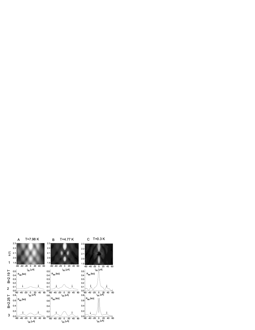
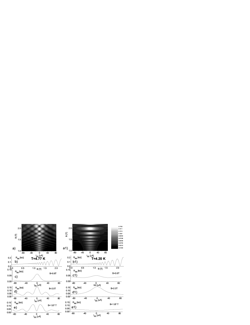
Figure 1 presents the magnetoresitance of two 2D electron systems with approximately the same electron density but with different electron lifetime . The left panel, Figs. 1(a)-1(e), shows data taken at temperature = 4.77 K for sample N1 with = 4 (ps). Figure 1(a) demonstrates an overall behavior of the differential resistance at different dc currents from -80 to 80 (A) and magnetic fields from 1 to 2.25 T. Taken at zero dc bias [ = 0 (A)] vertical cut of the 2D plot corresponds to the linear response of the system. The cut, extended to zero magnetic field, is shown in Fig. 1(b). The figure demonstrates well-known Shubnikov de Haas (SdH) oscillations of the resistance. These oscillations are periodic in the inverse magnetic field . Figure 1(c) demonstrates a horizontal cut of the 2D plot, which is taken at magnetic field = 0.6 T. At this magnetic field the SdH oscillations are absent as shown in Fig. 1(b). The strong decrease of the resistance with the dc bias is due to quantal heating, which is studied for this sample in detail inRef. vitkalov2009 (see also Ref. gusev2009 ). Figure 1(d) presents another dependence of the resistance on the dc bias. The dependence is taken at a maximum of SdH oscillations and corresponds to a horizontal cut of the 2D plot at B = 2 T. Figure 1(d) shows oscillations of the resistance with the dc bias. Figure 1(e) shows a dc bias dependence of the resistance taken at minimum of SdH oscillations at B = 1.87 T. Figure 1(e) demonstrates oscillations, which are complementary to the oscillations shown in Fig. 1(d). Sample N2 exhibits similar oscillations (not shown). The oscillations presented in Figs. 1(a),1(d) and 1(e) are the main subject of this paper stud2011 .
The right panel of Fig. 1 presents data obtained for sample N3 with similar electron density but with considerably shorter quantum scattering time = 1 (ps). The data are taken at temperature = 4.2 K. Figures 1(a1)-1(e1) demonstrate dependencies taken at the same conditions as the dependencies presented in Figures 1(a)-1(e). Due to the shorter time the Landau levels in the sample N3 are considerably broader than the quantum levels in the sample N1 and overlap substantially at = 0.6 (T) (see Fig.2 in Ref.vitkalov2009 ). In result shown in Fig. 1(c1) resistance variations are considerably smaller the one shown in Fig.1( c) dmitriev2005 ; vitkalov2009 . Figures 1(a1), 1(d1) and 1(e1) exhibit qualitatively different behavior: sample N3 does not show any oscillations with the dc bias.
Figure 2 demonstrates the effect of temperature on these oscillations. Figures 2(a1), 2(b1) and 2(c1) present the dependence of the differential resistance on magnetic field and dc bias taken at different temperatures as shown. The amplitude and shape of the oscillations depend on the temperature but the positions of the oscillations are essentially the same at different temperatures. At the lowest temperature = 0.3 (K) spin splitting of the Landau levels is observed. The splitting makes correlations between different curves less obvious. Figures 2(a2), 2(b2) and 2(c2) present horizontal cuts of the corresponding 2D plots 2(a1), 2(b1) and 2(c1) taken at magnetic field = 2.19 Tesla. At this magnetic field a maximum of SdH oscillations, which correspond to a spin polarized Landau level, is observed at = 0.3 (K). The cuts indicate maximums at around +35 and -35 (A) for all three temperatures. Arrows mark the maximums. The magnitude of the oscillations increases as the temperature decrease. Figures 2(a3), 2(b3) and 2(c3) present horizontal cuts taken at magnetic field B = 2.25 (T). These cuts correspond to a SdH resistance maximum at high temperatures, which evolves into a minimum at lowest temperature = 0.3 (K) at which the spin splitting is larger the temperature. Two cuts taken at T = 7.98 (K) and at the T = 4.75 (K) [Figs. 2(a3) and 2(b3)] demonstrate good correlation. At lowest temperature the resistance demonstrates minimum at zero dc bias and maximums at +35 and -35 (A) are not observed.
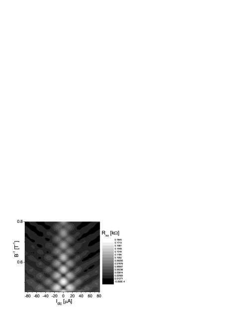
Figure 3 presents dependence of the differential resistance on the inverse magnetic field and dc bias for sample N1. The plot emphasizes the periodicity of the observed oscillations with respect to both the dc bias and the inverse magnetic field . The figure indicates that the positions of the oscillations with respect to the dc bias do not change considerably with almost two times variation of the magnetic field.
Figure 4(a) presents vertical cuts of Fig.3 taken at different dc biases, which are close to maximums and minimums shown on Fig.1(d). The figure demonstrates that the periodic oscillations at = -32.5 and -71.1 A are in phase whereas the oscillations at = -12.5 and -53.8 A are 180∘ shifted with respect to SdH oscillations at zero dc bias. Figure 4(b) presents a Fourier spectrum of the oscillations at = 0 and -32.5 A. The inset shows a dependence of the amplitude of the first harmonic of the oscillations on the dc bias. The experiment indicates a reduction of the oscillations with the dc bias increase.

Figures 3 and 4 demonstrates strong correlation of the dc biased-induced oscillations with the quantum oscillations at zero dc bias (SdH oscillations). This is an indication that these oscillations have a common origin. Below we consider a model, in which the oscillations are induced by spatial variations of the number of occupied Landau levels across the Hall bar sample.
IV IV. Model and Discussion
Shubnikov-de Haas oscillations occur due to quantization of electron spectrum in a magnetic field shoenberg1984 . With an increase of the magnetic field, energy gaps between Landau levels increase and the top occupied Landau level intersects the Fermi energy . At this condition resistivity of the electron systems is at a maximum. When the Fermi energy is between two Landau levels the resistivity is at a minimum. Thus the resistance oscillates with variations of the number of the Landau levels occupied by electrons.
We propose that the dc bias-induced oscillations also occur due to a variation of the electron filling factor but, in contrast to SdH oscillations, the variation appears across the sample and is related to a spatial change of electron density . If the change is comparable with the number of electron states in a Landau level , then one should expect a variation of the electron resistivity. As shown below the spatial variation of the resitivity leads to oscillations of the sample resistance.
A simple electrostatic estimation demonstrates that in a vacuum the variation of electron density creates a voltage, which is on several orders of magnitude stronger than the one observed in the experiment. The estimation dictates, therefore, the presence of a strong screening of electric charges in the samples. The proposed model assumes that the screening is due to Xelectrons, which are located near the conducting 2D layer.
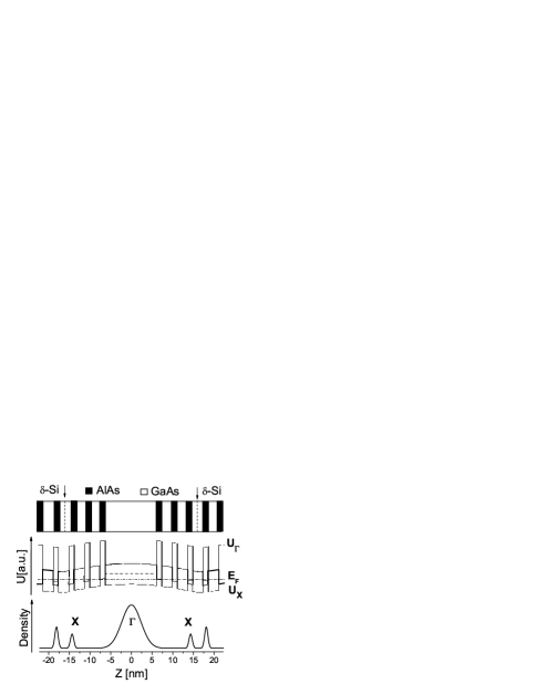
Figure 5 shows a schematic diagram of our samples. The conducting GaAs quantum well is sandwiched between two layers of AlAs/GaAs superlattices (SLs) of the second kind fried1996 . The main purpose of the X electrons is to enhance the electron mobility by screening the charged impurities near the conducting 2D layer. The parameters of the superlattices are adjusted to set the system close to a metal-insulator transition. At this condition the barely conducting SL layers efficiently screen electric charges and do not contribute considerably to the overall conductivity of the structure.
To estimate parameters relevant to the screening of the electron density we consider the superlattice as a metallic sheet placed at a distance from the conducting layer. A spatial variation of the electron density induces a variation of the voltage across the layer: , where is capacitance of the structure per unit area, is lattice permittivity, and is permittivity of free space. A typical electric potential in the present experiments is = 60 mV at = 2 (T). This yields = 39 (nm). This distance is comparable with the thickness of the superlattice: 27-80 (nm).
Electric contacts connect the GaAs and the SL layers. Thus the system is considered as a set of parallel conductors. At zero magnetic field the distribution of the electric potential driving the current is the same in all layers due to the same shape of the conductors. That is to say at B = 0 the potential difference between different layers is absent. In the poorly conducting SL layers the electric current is several order of magnitude smaller than the one in the highly conducting GaAs quantum well.
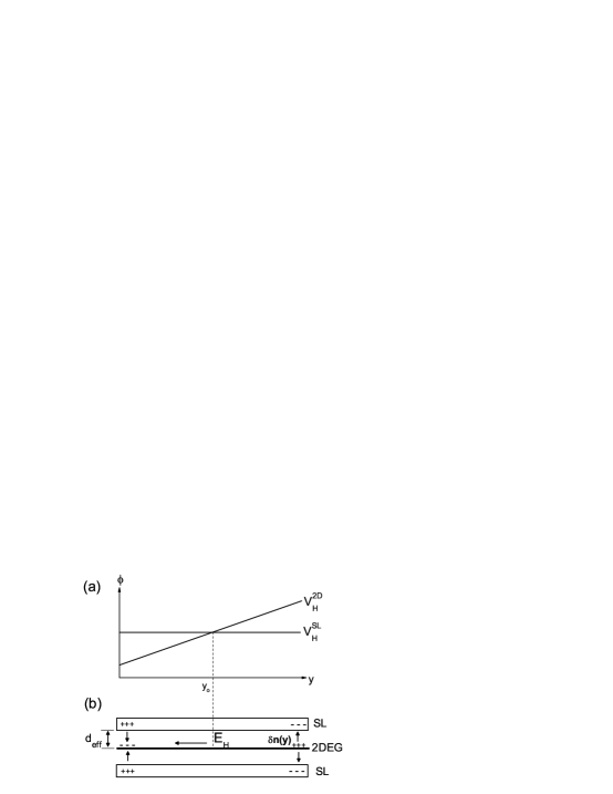
The layers have a different distribution of the electric potential in a strong magnetic field, at which and , where and are transport times in the GaAs and in the SL layers. The distribution is shown in Fig. 6(a) for a small total current (linear response). At the electric field in the GaAs layer is almost perpendicular to the current due to the strong Hall effect. In contrast, the very small electric current in the SL layer induces a Hall voltage, which is negligible. The Hall voltages are shown in the Fig. 6(a). Figure 6(b) presents distribution of electric charges in the structure. Electric charges are accumulated near the edges of the 2D highly conducting GaAs layer, inducing the Hall electric field . The charges are partially screened by charges accumulated in the conducting SL layers.
Due to the small Hall voltage and the absence of the electric current across the system the change of the electric potential in the SL layer is negligibly small. Below we consider the potential as a constant. Due to a finite screening length in the SL layer the charge accumulation occurs at a distance . Below we approximate the charge distribution by a charged capacitor with an effective distance between conducting plates.
A simplified model of the observed oscillations is presented below. The model considers a long 2D Hall bar with a width shashkin1986 ; dyakonov1990 . Electric current is in the direction and the Hall electric field is in the direction. In a long conductor the electric field is independent on , due to the uniformity of the system in direction:
| (1) |
For a steady current Maxwell equations yield:
| (2) |
Equations (1) and eq.(2) indicate, that the component of the electric field is the same at any location: const.
Boundary conditions and the continuity equation require that the density of the electric current in direction is zero: and therefore,
| (3) |
where and are longitudinal and Hall components of the resistivity tensor ziman . We approximate the SdH oscillations of the resistivity by a simple expression ando :
| (4) |
where is Drude resistivity and describes the amplitude of the quantum oscillations. At a SdH maximum (minimum) filling factor is half integer (integer).
An electrostatic evaluation of the voltage between conducting layers, shown in Fig.6(b), yields:
| (5) |
where and are electric potentials of the GaAs [2D electrong as (2DEG)] and superlattice (SL) layers, and is permittivity of the SL layer. Expressing the electron density in terms of electric potential from Eq.5 and substituting the relation into Eq.(4) one can find dependence of the resistitivity on the electric potential: .
The relation together with Eq.(3) yields:
| (6) |
Separation of the variables and and subsequent integration of Eq.(6) between two sides of the 2D conductor ( direction) with corresponding electric potentials and yield the following result:
| (7) |
where is a width of the sample. Taking into account that longitudinal voltage is , where is a distance between the potential contacts, and the Hall voltage [see Eq.(3)], the following relation is obtained:
| (8) |
, where is Drude resistance.
Equation 8 is simplified further for filling factors corresponding to a minimum or a maximum of SdH oscillations. In this case the voltage is expected to be an asymmetric function of the relative position with respect to the center of the sample : .pikus1992 An example of the asymmetric distribution of the electric potential is shown in Fig. 6(a) for small currents. In this case and the argument of the cosine in Eq.(8) becomes independent on the electric current. For the integer (a SdH minimum) and half-integer (a SdH maximum) filling factors the differential resistance is found to be
| (9) |
where .
Equation 9 demonstrates periodic oscillations of the differential resistance with both the electric current and the inverse magnetic field (). The period of the current induced oscillations does not depend on the magnetic field and temperature in accordance with the experiment. The phase difference between oscillations starting at the SdH maxima and minima is , which is in agreement with Figs.1(d) and 1(e). The period of the oscillations shown above (A) indicates that the screening occurs at an effective distance 36 (nm). The distance is comparable with thicknesses of the SL layers: 27 and 76 nm.
The 1/B periodic oscillations of the resistance at (i=1,2…) are in-phase with SdH oscillations [I=0 (A)] whereas a phase of the oscillations at is shifted by with respect to the phase of the SdH oscillations. This is in agreement with the results presented in Fig.4(a).
Figures 1(d), 1(e), and 4(b) show that the amplitude of the oscillations depends on the current: the oscillations are weaker at a higher current. This behavior is beyond the simplified model presented above. There are several possible mechanisms which may affect the amplitude of the quantum oscillations. One of the possibilities is the Joule heating. The heating may significantly decrease the amplitude of quantum oscillations romero2008 ; vitkalov2009 reducing the magnitude of the spatial variations of the local resistivity.
The current induced oscillations are absent in samples N3 and N4. These samples have the same electron densities and mobilities as samples N1 and N2 but four times shorter quantum scattering time . We suggest that the observed significant difference in the and the absence of the oscillations is result of a less effective screening in the SL layers of the samples N3, N4. A weaker screening is expected in conducting superlattices, which are closer to the metal-insulator transition. In this case the screening of an electric charge occurs at a larger distance due to smaller density of conducting states. Thus the effective thickness and therefore the period can be significantly larger in weaker conducting SL layers.
V V. Conclusion
Oscillations of differential resistance are observed in response to both electric current and magnetic field, which is applied perpendicular to 2D electrons in GaAs quantum wells. The oscillations are periodic with the current and with the inverse magnetic field. The period of the current induced oscillations does not depend on magnetic field and temperature. The SdH oscillations are a part of the set at zero dc bias. The proposed model considers spatial variations of the electron filling factor, which are induced by applied dc bias, as the origin of the resistance oscillations. The present experiment, thus, indicates a feasibility of the significant re-population of Landau levels by the electric current.
VI Acknowledgements
S. V. thanks I. L. Aleiner for valuable help with the theoretical model and discussion. S. V. thanks Science Division of CCNY, CUNY Office for Research, PSC-CUNY Research Award Program (Project No. 63413-0041) and NSF (Grant No. DMR 1104503) for support of the experiments. A. A. B. thanks the Russian Foundation for Basic Research, Project No. 11-02-00925.
References
- (1) M.A. Zudov, R. R. Du, J. A. Simmons, and J. L. Reno, Phys. Rev. B 64,201311(R) (2001).
- (2) P.D. Ye, L. W. Engel, D.C. Tsui, J. A. Simmons, J. R. Wendt, G. A. Vawter, and J. L. Reno, Appl. Phys. Lett. 79,2193 (2001).
- (3) C. L.Yang, J. Zhang, and R. R. Du, J. A. Simmons and J. L.Reno, Phys. Rev. Lett. 89, 076801 (2002).
- (4) S. I. Dorozhkin, JETP Lett. 77, 577 (2003).
- (5) R. L. Willett, L. N. Pfeiffer, and K. W. West, Phys. Rev. Lett. 93 026804 (2004).
- (6) R.G. Mani, J. H. Smet, K. von Klitzing, V. Narayanamurti, W. B. Johnson, and V. Umansky, Phys. Rev. 69, 193304 (2004).
- (7) I. V. Kukushkin, M. Ya. Akimov, J. H. Smet, S. A. Mikhailov, K. von Klitzing, I. L. Aleiner, and V. I. Falko, Phys. Rev. Lett. 92, 236803 (2004).
- (8) S. A. Studenikin, M. Potemski, A. Sachrajda, M. Hilke, L. N. Pfeiffer, and K. W. West, Phys. Rev. B 71, 245313, (2005).
- (9) A. A. Bykov, Jing-qiao Zhang, Sergey Vitkalov, A. K. Kalagin, and A. K. Bakarov Phys. Rev. B 72, 245307 (2005).
- (10) A. A. Bykov, A. K. Bakarov, D. R. Islamov, A. I. Toropov, JETP Lett. 84, 391 (2006).
- (11) Jing-qiao Zhang, Sergey Vitkalov, A. A. Bykov, A. K. Kalagin, and A. K. Bakarov Phys. Rev. B 75, 081305(R) (2007).
- (12) W. Zhang, H.-S. Chiang, M. A. Zudov, L.N. Pfeiffer, and K.W. West, Phys. Rev. B 75, 041304(R) (2007).
- (13) K. Stone, C. L. Yang, Z. Q. Yuan, R. R. Du, L. N. Pfeiffer, and K. W. West Phys. Rev. B 76, 153306 (2007).
- (14) S. A. Studenikin, A. S. Sachrajda, J. A. Gupta, Z. R. Wasilewski, O. M. Fedorych, M. Byszewski, D. K. Maude, M. Potemski, M. Hilke, K. W. West, and L. N. Pfeiffer, Phys. Rev. B 76, 165321 (2007).
- (15) A.T. Hatke, H.-S. Chiang, M.A. Zudov, L.N. Pfeiffer, and K.W. West, Phys. Rev. B 77, 201304(R) (2008).
- (16) A. A. Bykov, D. R. Islamov, A. V. Goran, and A. I. Toropov, JETP Lett. 87, 477 (2008).
- (17) N. Romero Kalmanovitz, A. A. Bykov, Sergey Vitkalov, and A. I. Toropov Phys. Rev. B 78, 085306 (2008).
- (18) S. Wiedmann, G. M. Gusev, O. E. Raichev, T. E. Lamas, A. K. Bakarov, and J. C. Portal Phys. Rev. B 78, 121301 (2008).
- (19) A. T. Hatke, M. A. Zudov, L. N. Pfeiffer, and K. W. West Phys. Rev. B 79, 161308 (2009).
- (20) A. T. Hatke, M. A. Zudov, L. N. Pfeiffer, and K. W. West Phys. Rev. Lett. 102, 066804 (2009).
- (21) S. I. Dorozhkin, I. V. Pechenezhskiy, L. N. Pfeiffer, K. W. West, V. Umansky, K. von Klitzing, and J. H. Smet Phys. Rev. Lett. 102, 036602 (2009).
- (22) Jing Qiao Zhang, Sergey Vitkalov, and A. A. Bykov Phys. Rev. B 80, 045310 (2009).
- (23) S. A. Vitkalov, International Journal of Modern Physics B 23, 4727 (2009).
- (24) N. C. Mamani, G. M. Gusev, O. E. Raichev, T. E. Lamas, and A. K. Bakarov, Phys. Rev. B 80, 075308 (2009).
- (25) A. C. Durst, S. Sachdev, N. Read, and S. M. Girvin, Phys. Rev. Lett. 91, 086803 (2003).
- (26) V. I. Ryzhii Sov. Phys. Solid State 11, 2078 (1970).
- (27) P. W. Anderson and W. F. Brinkman, cond-mat/0302129.
- (28) J. Shi and X. C. Xie, Phys. Rev. Lett. 91, 086801 (2003).
- (29) X. L. Lei and S. Y. Liu, Phys. Rev. B 72, 075345 (2005).
- (30) J. Dietel, L. I. Glazman, F. W. J. Hekking, and F. von Oppen Phys. Rev. B 71, 045329 (2005).
- (31) J. Inarrea and G. Platero Phys. Rev. B 72, 193414 (2005)
- (32) M. G. Vavilov and I. L. Aleiner Phys. Rev. B 69, 035303 (2004).
- (33) I. A. Dmitriev, M.G. Vavilov, I. L. Aleiner, A. D. Mirlin, and D. G. Polyakov, Phys. Rev. B 71, 115316 (2005).
- (34) J. Alicea, L. Balents, M.P.A. Fisher, A. Paramekanti, L. Radzihovsky, Phys. Rev. B 71, 235322 (2005).
- (35) E. E. Takhtamirov and V. A. Volkov JETP 104, 602 (2007).
- (36) M.G. Vavilov, I.L Aleiner, and L.I. Glazman, Phys.Rev. B 76,115331 (2007).
- (37) I. A. Dmitriev, A. D. Mirlin, and D. G. Polyakov,Phys. Rev B 75, 245320 (2007).
- (38) R. G. Mani, V.Narayanamurti, K. von Klitzing, J. H. Smet, W. B. Jonson, and V. Umansky, Nature(London) 420, 646 (2002).
- (39) M.A. Zudov, R. R. Du, L. N. Pfeiffer, and K. W. West, Phys. Rev. Lett. 90, 046807 (2003).
- (40) W. Zhang, M.A. Zudov, L. N. Pfeiffer, and K. W. West Phys. Rev. Lett. 98,106804 (2007).
- (41) A. A. Bykov, Jing-qiao Zhang, Sergey Vitkalov, A. K. Kalagin, and A. K. Bakarov Phys. Rev. Lett. 99, 116801 (2007).
- (42) W. Zhang, M. A. Zudov, L.N. Pfeiffer, and K.W. West, Phys. Rev. Lett. 100, 036805 (2008).
- (43) A. A. Bykov, E. G. Mozulev, and S. A. Vitkalov, JETP Lett. 92, 475 (2010).
- (44) A. T. Hatke, H.-S. Chiang, M. A. Zudov, L. N. Pfeiffer, and K. W. West Phys. Rev. B 82, 041304 (2010).
- (45) G. M. Gusev, S. Wiedmann, O. E. Raichev, A. K. Bakarov, and J. C. Portal Phys. Rev. B 83, 041306 (2011).
- (46) A. V. Andreev, I. L. Aleiner, and A. J. Millis, Phys.Rev. Lett. 91, 056803 (2003).
- (47) A. Auerbach, I Finkler, B. I. Halperin, and A. Yacoby, Phys. Rev. Lett. 94, 196801 (2005).
- (48) K. J. Friedland, R. Hey, H. Kostial, R. Klann, and K. Ploog, Phys. Rev. Lett. 77, 4616 (1996).
- (49) Interesting inversion of the phase of SdH oscillations with bias was reported recently. S. A. Studenikin, G. Granger, A. Kam, A. S. Sachrajda, Z. R. Wasilewski, P. J. Poole, preprint http://lanl.arxiv.org/abs/1012.0043. It may have similar origin as the oscillations presented in this paper.
- (50) D. Shoenberg Magnetic oscillations in metals, (Cambridge University Press, 1984).
- (51) A. A. Shashkin, V. T. Dolgopolov, and S. I. Dorozhkin, Sov. Phys. JETP 64, 1124 (1986).
- (52) M. I. Dyakonov, Solid State Comm. 78, 817 (1991).
- (53) J. M. Ziman Principles of the theory of solids, (Cambridge at the University Press, 1972).
- (54) T. Ando, A. B. Fowler, and F. Stern, Rev. of Mod. Phys. B 54, 437 (1982).
- (55) M.I. Dyakonov and F. G. Picus, Solid State Comm. 83, 413 (1992).