Sub-micron normal-metal/insulator/superconductor tunnel junction thermometer and cooler using Nb
Abstract
We have successfully fabricated Cu/AlOx-Al/Nb normal-metal/insulator/superconductor tunnel junction devices with a high value of the superconducting gap (up to mV), using electron-beam lithography and angle evaporation techniques in the sub-micron scale. The subgap conductance of these junctions shows the expected strong temperature dependence, rendering them suitable for thermometry all the way from 100 mK to 6 K. In addition, some direct electronic cooling of the normal metal was also seen at bias values near the gap edge. The device performance was strongly influenced by the details of the Al layer geometry, with lateral spilling of the aluminium giving rise to strong extra subgap features, and the thickness of Al layer affecting the proximised superconducting gap value of the superconducting Al/Nb bilayer.
Normal-metal-insulator-superconductor (NIS) tunnel junction devices have already proven as promising solid state coolers Muhonen, Meschke, and Pekola (2012); Giazotto et al. (2006); Koppinen and Maasilta (2009); Miller et al. (2008), accurate low temperature thermometers and sensitive bolometers Giazotto et al. (2006); Koppinen, Kühn, and Maasilta (2009); Schmidt et al. (2005), and near-ideal single electron transistorsPekola et al. (2008); Saira et al. (2012). Some active research on such devices is aimed at enhancing the cooling power at sub-300 mK temperaturesO’Neil et al. (2012), but increasing the operational range in temperature by changing the superconducting material (gap ) from the traditional aluminum has not been very successful yet, although a promising new alternative is to use SIS’ structures, instead Quaranta et al. (2011).
To extend the range of NIS devices beyond the operational range of Al, which has an upper limit for thermometry at 1.5 K and the maximum cooling power at 300 mK, one should consider the elemental metal with highest gap, niobium ( 9 K). It is already routinely used for SIS tunnel junction applications in SQUIDs, radiation detectors and digital electronics van Duzer and Turner (1999). In those applications, fairly large micron-scale junctions can typically be tolerated, and fabrication usually proceeds by the robust Nb/Al/AlOx/Nb trilayer deposition and etching techniques Gurvitch, Washington, and Huggins (1983); Tolpygo et al. (2007), where Nb and Al are typically sputter deposited, and the high quality AlOx barrier is thermally grown on a thin 10 nm Al layer. This process typically yields a high gap 1.3 mV and a near bulk 9 K Morohashi et al. (1985); Dolata et al. (2005).
In contrast, for single-charge devices and for small thermometers and bolometers, sub-micron scale junctions are desired. They are easier to fabricate using angle-evaporation and lift-off Dolan and Dunsmuir (1988), although a successful but more complex sub-micron Nb trilayer Josephson junction process has also been demonstrated Dolata et al. (2005). The quality of evaporated Nb, unfortunately, has turned out to be quite sensitive to the exact chamber and substrate conditions, such as vacuum level, evaporation speed, substrate to Nb crucible distance and especially to the type of resist used Kim et al. (2002); Pekola et al. (1999); Dolata et al. (2003); Harada et al. (1994); Dubos et al. (2000); Hoss, Strunk, and Schönenberger (1999). Problems with standard polymer resists are typically attributed to decomposition and outgassing during Nb evaporation, leading to the suppression of and .
Here, we demonstrate that a fairly simple angle-evaporation process can, nevertheless, be used to fabricate good quality micron to submicron scale NIS tunnel junctions with Al/Nb bilayer as the superconductor and Cu as the normal metal, and that the junctions can be used for sensitive thermometry up to 6 K, with a full theoretical understanding of the response. Electronic cooling was also demonstrated near the gap edge at an elevated temperature range compared to standard Al coolers. The only previous work on Cu/AlOx/Nb NIS junctions used a trilayer technique to produce only large-scale (m) junctions, and reported non-ideal responsivity with no cooling Castellano et al. (1997); Leoni et al. (2003).
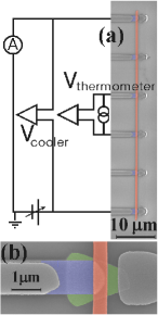
A scanning electron micrograph of the Nb/Al-AlOx/Cu multiple NIS junction sample fabricated using electron beam lithography (EBL) and shadow-evaporation technique is shown in Figure 1(a), with a close-up of the junction area in Fig. 1 (b). Oxidized silicon serves as the substrate. A dual layer PMMA/P(MMA–MAA) positive resist recipe was used for the lithography, forming an undercut structure not . The metal evaporation was performed in an ultra high vacuum chamber with an electron-beam source. First, 20 nm of Nb was evaporated from an angle of 30 degrees with respect to the plane of the substrate. After the deposition of Nb, we waited 15 minutes for the Nb to cool down. This leads to an improvement in the quality of the junctionSimon et al. (1992). This was followed by Al evaporation (5-20 nm thickness), whereby half of the total Al to be deposited was evaporated from the same 30 degree angle as that of Nb, while the other half was deposited from -30 degrees. The tip of the Nb electrode was designed to be slightly tapering, as shown in Figure 1(b), to improve Al coverage. The idea of the Al deposition from two opposite angles was to achieve uniform Al coverage, even on the edges of the Nb electrode. The Al was then oxidized in-situ at 350 mbar for 25 minutes. Finally, 30-50 nm copper was evaporated from the normal angle. The chamber pressure during the metal deposition was 1.510-8 mbar, and the evaporation rates for Nb, Al and Cu were typically 0.45, 0.1 and 0.1 nm/s, respectively.
We have succesfully made samples with four different thicknesses () of Al (Cu) layers, namely 7 (35), 10 (40), 15 (30) and 20 (50) nm, while Nb was 20 nm thick in all cases. An attempt was made to use a 5 nm Al layer, as well, but the Al coverage was not complete anymore in that case. The thickness and the line width (1 m) for the Nb electrodes were chosen so that on one hand, they could still show and close to the bulk values, while on the other hand, it would still be possible to cover the Nb layer with a thin film of Al. The dimensions of the Cu wire were typically 55 m 400 nm 35 nm. We have also confirmed the earlier observations that and of shadow-evaporated Nb depend strongly of the Nb thickness, line width and deposition conditions Pekola et al. (1999); Kim et al. (2002); Dolata et al. (2003); Harada et al. (1994); Dubos et al. (2000); Hoss, Strunk, and Schönenberger (1999); Bose et al. (2005); Park and Geballe (1986).
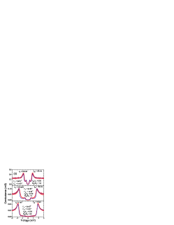
The measurements were carried out using a He3-He4 dilution refrigerator with a base temperature of 60 mK. The measurement lines had two RC filter stages, one at 4 K and the other at 60 mK, and microwave filtering between the RC filters was achieved with the help of Thermocoax cables connecting the two RC filter stages. Figure 1(c) shows the differental conductance-voltage () characteristics, measured at a bath temperature of 150 mK, for samples with three different thicknesses (7, 10 and 20 nm) of the Al layer. Clearly, the characteristics show a double gapped structure (two sets of conductance peaks), which evolves with the Al thickness. This can be explained as follows: As there is a slight overspill of Al on top of the Nb to ensure complete coverage of the Nb (avoiding a direct Nb-Cu contact), part of the current tunnels into Cu through the overspill region where Al is not fully proximised, as the overspill length can be of the same order of magnitude or larger than the coherence length. Thus, each physical Nb-Al-AlOx-Cu junction can be modelled as two electrical junctions in parallel, the main one (J1) with Al directly on top of Nb, and the other (J2) the overspill region without Nb. The gap value of the first junction () is that of Al proximised by Nb in the perpendicular direction, whereas the gap value of the overspill junction () is that of Al proximised by Nb in the lateral (in-plane) direction, which in the case of large overspill would lead to an unproximized Al gap.
The total current as a function of voltage can then be written as a sum of two junction currents, where each individual current is given by the usual expression Giazotto et al. (2006) , where is the tunneling resistance of junction , is the Fermi function in either the superconducting or the normal electrode, and is the normalized superconducting quasiparticle density of states of junction . Here, we use the expression , which for Al junctions has been shown Dynes et al. (1984); Pekola et al. (2010) to accurately describe the broadening of the DOS singularity, where is the Dynes parameter describing the broadening, and is the superconducting energy gap, with its temperature dependence written explicitly. Intuitively, it is clear that this model produces peak features at two voltages and , but the specific shape of the conductance curve is determined by the ratio of the two gaps () and the ratio of the tunnelling resistances ().

We have succesfully used the parallel junction model to fit the conductance plots of Figure 1 (c). The larger gap (perpendicularly proximized Al/Nb) increases with decreasing from 0.45 and 0.9 up to 1 mV for = 20, 10 and 7 nm, respectively. To our knowledge, 1 mV is the highest ever gap reported for a tunnel junction with a Nb electrode fabricated by angle evaporation Dolata et al. (2003); Kim et al. (2002); Harada et al. (1994). From the fits in Figure 1(c), we also find that 0.30-0.35 for all samples. On the other hand, the ratio of the tunneling resistances is not constant, but varies by an order of magnitude between 2-20, reflecting the different relative strengths of the two conductance peaks. Physically, this results from differing amounts of Al overspill between the three samples. The Al overspill for the samples with 10 and 20 nm thick Al layer is about 200-300 nm. This makes the two junction areas and thus and comparable, leading to clear exhibition of the small gap feature in Fig. 1 (c). For the sample with 7 nm thick Al, we managed to reduce the lateral spill to 100 nm by improving the Al to Nb layer alignment, and were thus able to suppress the small gap features significantly. The measured of the sample with = 7 nm with was 6 K, leading to a relation , in agreement with the literature for pure Nb van Duzer and Turner (1999). Finally, the relative Dynes parameter values stay approximately constant regardless of the Al thickness with values , and . is consistent with previous studies in Al Koppinen, Kühn, and Maasilta (2009); Pekola et al. (2010); Greibe et al. (2011), but , interestingly, is smaller than previously reported for pure Nb Proslier et al. (2008).
The temperature dependence of the current-voltage and conductance-voltage characteristics of the sample with 7 nm Al are shown in Fig. 2, with other samples showing similar behavior (not shown). The low bias region mV is dominated by the excess sub-gap current of the gap edge (parametrized by ), and has a weak temperature dependence. However, at higher bias voltages, a clear temperature dependence is seen, as expected for ideal NIS junctions Giazotto et al. (2006). The theoretical curves based on the parallel junction model fit the data well at all temperatures, if self-cooling, heating and electron-phonon (e-p) coupling in the Cu wire are taken into account Chaudhuri and Maasilta (2012).
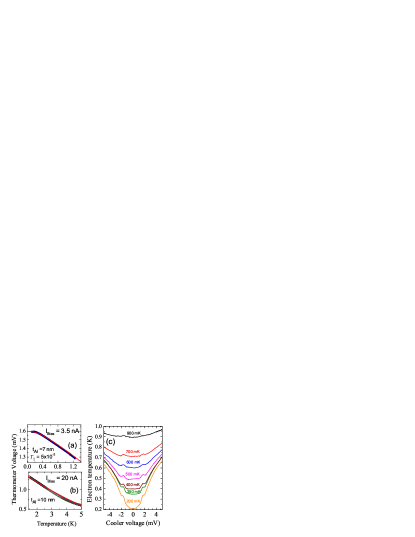
As can be seen from Fig. 2, the junctions can be used for thermometry by biasing with constant current above the excess sub-gap current level [ nA in Fig. 2 (a)], and by measuring the temperature dependent voltage. The response of two of the devices ( = 7 and 10 nm) to changes in bath temperature are shown in Figs. 3(a) and (b), along with the corresponding theoretical fits, assuming that the electron temperature is equal to the bath temperature (no self-cooling, heating and e-p coupling). Clearly, our devices have good responsivity 0.2-0.3 mV/K all the way from 200 mK to 5 K, and some responsivity left up to K (not shown). We also see that the fits are good for these bias points even without the thermal effects taken into account, so that we have full understanding of the temperature response of the devices. The responsivity is the same as in Al-based NIS thermometers as expected from the theory, but the major advantage of Nb-based NIS thermometry is that the operational range is extended to much higher temperatures.
In addition to thermometry, we have investigated the electronic cooling performance of the device with = 7 nm, shown in Figure 3(c), by measuring the temperature of the Cu island with one SINIS pair as a function of the bias voltage across a second (cooler) SINIS pair [the measurement circuit shown in Fig. 1 (a)]. A clear cooling dip is observable at all values of mK - 900 mK near the second gap edge at mV. Unfortunately, there is also observable heating in the subgap region (especially at low ), caused by the excess subgap currents, so that no cooling below the base temperature was obtained yet. However, the observed value of does not theoretically prevent reaching temperatures below , and as this was the first demonstration of Nb-based NIS cooling, we believe that there is room for improvement. For example, the junction size and geometry could be improved, the overspill could be reduced even further, and the normal metal volume could be reduced by at least an order of magnitude.
In conclusion, we have successfully fabricated submicron scale Nb-Al-AlOx-Cu based NIS tunnel junctions using e-beam lithography and angle evaporation, with a gap 1 mV and broadening parameter . The devices have good thermometric response in the temperature range between 200 mK to 5 K. Direct electronic cooling was observed at all bath temperatures between 200 mK and 900 mK, but not below the base temperature yet.
This research was supported by the Academy of Finland project number 128532.
References
- Muhonen, Meschke, and Pekola (2012) J. T. Muhonen, M. Meschke, and J. P. Pekola, Rep. Prog. Phys. 75, 046501 (2012).
- Giazotto et al. (2006) F. Giazotto, T. T. Heikkilä, A. Luukanen, A. M. Savin, and J. P. Pekola, Rev. Mod. Phys. 78, 217 (2006).
- Koppinen and Maasilta (2009) P. J. Koppinen and I. J. Maasilta, Phys. Rev. Lett. 102, 165502 (2009).
- Miller et al. (2008) N. A. Miller, G. C. O Neil, J. A. Beall, G. C. Hilton, K. D. Irwin, D. R. Schmidt, L. R. Vale, and J. N. Ullom, Appl. Phys. Lett. 92, 163501 (2008).
- Koppinen, Kühn, and Maasilta (2009) P. J. Koppinen, T. Kühn, and I. J. Maasilta, J. Low Temp. Phys. 154, 179 (2009).
- Schmidt et al. (2005) D. R. Schmidt, K. W. Lehnert, A. M. Clark, W. D. Duncan, K. D. Irwin, N. Miller, and J. N. Ullom, Appl. Phys. Lett. 86, 053505 (2005).
- Pekola et al. (2008) J. P. Pekola, J. J. Vartiainen, M. Möttönen, O.-P. Saira, M. Meschke, and D. V. Averin, Nat. Phys. 4, 120 (2008).
- Saira et al. (2012) O.-P. Saira, A. Kemppinen, V. F. Maisi, and J. P. Pekola, Phys. Rev. B 85, 012504 (2012).
- O’Neil et al. (2012) G. C. O’Neil, P. J. Lowell, J. M. Underwood, and J. N. Ullom, Phys. Rev. B 85, 134504 (2012).
- Quaranta et al. (2011) O. Quaranta, P. Spathis, F. Beltram, and F. Giazotto, Appl. Phys. Lett. 98, 032501 (2011).
- van Duzer and Turner (1999) T. van Duzer and C. W. Turner, Superconductive Devices and Circuits, 2nd Ed. (Prentice Hall, New Jersey, 1999).
- Gurvitch, Washington, and Huggins (1983) M. Gurvitch, M. A. Washington, and H. A. Huggins, Appl. Phys. Lett. 42, 472 (1983).
- Tolpygo et al. (2007) S. K. Tolpygo, D. Amparo, A. Kirichenko, and D. Yohannes, Supercond. Sci. Technol. 20, S341 (2007).
- Morohashi et al. (1985) S. Morohashi, F. Shinoki, A. Shoji, M. Aoyagi, and H. Hayakawa, Appl. Phys. Lett. 46, 1179 (1985).
- Dolata et al. (2005) R. Dolata, H. Scherer, A. B. Zorin, and J. Niemeyer, J. Appl. Phys. 97, 054501 (2005).
- Dolan and Dunsmuir (1988) G. J. Dolan and J. H. Dunsmuir, Physica B 152, 7 (1988).
- Kim et al. (2002) N. Kim, K. Hansen, J. Toppari, T. Suppula, and J. Pekola, J. Vac. Sci. Technol. B 20, 386 (2002).
- Pekola et al. (1999) J. Pekola, J. Kyynäräinen, M. Leivo, and A. Manninen, Cryogenics 39, 653 (1999).
- Dolata et al. (2003) R. Dolata, H. Scherer, A. B. Zorin, and J. Niemeyer, J. Vac. Sci. Technol. B 21, 775 (2003).
- Harada et al. (1994) Y. Harada, D. B. Haviland, P. Delsing, C. D. Chen, and T. Claeson, Appl. Phys. Lett. 65, 636 (1994).
- Dubos et al. (2000) P. Dubos, P. Charlat, T. Crozes, P. Paniez, and B. Pannetier, J. Vac. Sci. Technol. B 18, 122 (2000).
- Hoss, Strunk, and Schönenberger (1999) T. Hoss, C. Strunk, and C. Schönenberger, Microelectronic Engineering 46, 149 (1999).
- Castellano et al. (1997) M. G. Castellano, R. Leoni, G. Torrioli, P. Carelli, A. Gerardino, and F. Melchiorri, IEEE Trans. Appl. Supercond. 7, 3251 (1997).
- Leoni et al. (2003) R. Leoni, B. Buonomo, M. G. Castellano, F. Mattioli, D. Simeone, G. Torrioli, and P. Carelli, J. Appl. Phys. 93, 3572 (2003).
- (25) For the co-polymer layer, we have used commercially available P(MMA–MAA) resist diluted in acetic acid, while the top layer resist is PMMA diluted with anisole. The layer thicknesses were 500 and 450 nm, respectively, while the respective baking times were 15 and 5 minutes at a temperature of C. Before metal evaporation, the sample was cleaned in oxygen plasma for 30 seconds to get rid of organic impurities on the exposed substrate surfaces .
- Simon et al. (1992) W. Simon, E. K. Liebemann, M. Simon, and E. Bucher, J. Appl. Phys. 72, 4474 (1992).
- Bose et al. (2005) S. Bose, P. Raychaudhuri, R. Banerjee, P. Vasa, and P. Ayyub, Phys. Rev. Lett. 95, 147003 (2005).
- Park and Geballe (1986) S. I. Park and T. H. Geballe, Phys. Rev. Lett. 57, 901 (1986).
- Dynes et al. (1984) R. C. Dynes, J. P. Garno, G. B. Hertel, and T. P. Orlando, Phys. Rev. Lett. 53, 2437 (1984).
- Pekola et al. (2010) J. P. Pekola, V. F. Maisi, S. Kafanov, N. Chekurov, A. Kemppinen, Y. A. Pashkin, O.-P. Saira, M. Möttönen, and J. S. Tsai, Phys. Rev. Lett. 105, 026803 (2010).
- Greibe et al. (2011) T. Greibe, M. P. V. Stenberg, C. M. Wilson, T. Bauch, V. S. Shumeiko, and P. Delsing, Phys. Rev. Lett. 106, 097001 (2011).
- Proslier et al. (2008) T. Proslier, J. F. Zasadzinski, L. Cooley, C. Antoine, J. Moore, J. Norem, M. Pellin, and K. E. Gray, Appl. Phys. Lett. 92, 212505 (2008).
- Chaudhuri and Maasilta (2012) S. Chaudhuri and I. J. Maasilta, Phys. Rev. B 85, 014519 (2012).