All-Dielectric Optical Nanoantennas
Alexander E. Krasnok1,∗, Andrey E. Miroshnichenko2,∗∗,
Pavel A. Belov1,3, Yuri S. Kivshar1,2
1National Research University of Information Technologies, Mechanics and Optics, St. Petersburg 197101, Russia
2Nonlinear Physics Centre, Research School of Physics and Engineering, Australian National University, Canberra ACT 0200, Australia
3Queen Mary College, University of London, Mile End Road, London E1 4NS, United Kingdom
∗krasnokfiz@mail.ru, ∗∗aem124@physics.anu.edu.au
Abstract
We study in detail a novel type of optical nanoantennas made of high-permittivity low-loss dielectric particles. In addition to the electric resonances, the dielectric particles exhibit very strong magnetic resonances at the nanoscale, that can be employed in the Yagi-Uda geometry for creating highly efficient optical nanoantennas. By comparing plasmonic and dielectric nanoantennas, we demonstrate that all-dielectric nanoantennas may exhibit better radiation efficiency also allowing more compact design.
OCIS codes: (050.6624) Subwavelength structures; (250.5403) Plasmonics.
References and links
- [1] T. H. Taminiau, F. D. Stefani, and N. F. van Hulst, “Enhanced directional excitation and emission of single emitters by a nano-optical Yagi-Uda antenna,” Opt. Express 16, 10858–10866 (2008).
- [2] L. Novotny, “Optical antennas tuned to pitch,” Nature (London) 455, 887 (2008).
- [3] A. F. Koenderink, “Plasmon Nanoparticle Array Waveguides for Single Photon and Single Plasmon Sources,” Nano Lett. 9, 4228–4233 (2009).
- [4] T. Pakizeh, and M. Kall, “Unidirectional Ultracompact Optical Nanoantennas,” Nano Lett. 9, 2343–2349 (2009).
- [5] A. Devilez, B. Stout, and N. Bonod, “Compact Metallo-Dielectric Optical Antenna for Ultra Directional and Enhanced Radiative Emission,” ACS Nano 4, 3390–3396 (2010).
- [6] L. Novotny, and N. van Hulst, “Antennas for light,” Nat. Photon. 5, 83–90 (2010).
- [7] J. Dorfmuller, D. Dregely, M. Esslinger, W. Khunsin, R. Vogelgesang, K. Kern, and Harald Giessen, “Near-Field Dynamics of Optical Yagi-Uda Nanoantennas,” Nano Lett. 11, 2819–2824 (2011).
- [8] A. E. Miroshnichenko, I. S. Maksymov, A. R. Davoyan, C. Simovski, P. Belov and Y. S. Kivshar, “An arrayed nanoantenna for broadband light emission and detection,” Phys. Status Solidi RRL 5, 347–349 (2011).
- [9] C. Balanis, Antenna theory: Analysis and design (New York ; Brisbane: J. Wiley, 1982).
- [10] S. V. Boriskina, and B. M. Reinhard, “Adaptive on-chip control of nano-optical fields with optoplasmonic vortex nanogates,” Opt. Express 19, 22305–22315 (2011).
- [11] S. V. Boriskina, and B. M. Reinhard, “Spectrally and spatially configurable superlenses for optoplasmonic nanocircuits,” PNAS 108, 3147–3151 (2011).
- [12] A. B. Evlyukhin, C. Reinhardt, A. Seidel, B. S. Luk yanchuk, and B. N. Chichkov, “Optical response features of Si-nanoparticle arrays,” Phys. Rev. B 82, 045404 (2010).
- [13] A. E. Krasnok, A. E. Miroshnichenko, P. A. Belov, and Yu. S. Kivshar, “Huygens Optical Elements and Yagi Uda Nanoantennas Based on Dielectric Nanoparticles,” JETP Letters 94, 635 -640 (2011).
- [14] C.F. Bohren, and D.R. Huffman, Absorption and scattering of light by small particles (New York : Wiley, 1998).
- [15] A. E. Miroshnichenko, B. Luk’yanchuk, S. A. Maier, and Y. S. Kivshar, “Optically Induced Interaction of Magnetic Moments in Hybrid Metamaterials,” ACS Nano 6, 837-842 (2012).
- [16] E. Palik, Handbook of Optical Constant of Solids (San Diego, Academic, 1985).
- [17] O. Merchiers, F. Moreno, F. Gonzalez, and J. M. Saiz, “Light scattering by an ensemble of interacting dipolar particles with both electric and magnetic polarizabilities,” Phys. Rev. A 76, 043834 (2007).
- [18] M. Kerker, P. Scheiner, and D. D. Cooke, “The range of validity of the Rayleigh and Thomson limits for Lorenz-Mie scattering,” J. Opt. Soc. Am. 68, 135–137 (1978).
- [19] B. Rolly, B. Stout, S. Bidault, and N. Bonod, “Crucial role of the emitter particle distance on the directivity of optical antennas,” Opt. Lett. 36, 3368–3370 (2011).
- [20] L. Novotny, and B. Hecht, Principles of Nano-Optics (Cambridge University Press, New York, 2006).
- [21] H. Chew, “Transition rates of atoms near spherical surfaces,” J. Chem. Phys. 87, 1355–1360 (1987).
- [22] Yu-lin Xu, and Bo A. S. Gustafson, “A generalized multiparticle Mie-solution: further experimental verification,” J. Quant. Spectrosc. Radiat. Transfer 70, 395–419 (2001).
- [23] E. Dulkeith, M. Ringler, T. A. Klar, J. Feldmann, A. M. Javier, and W. J. Parak, “Gold Nanoparticles Quench Fluorescence by Phase Induced Radiative Rate Suppression,” Nano Lett. 5, 585-589 (2005).
- [24] B. Stout, A. Devilez, B. Rolly, and N. Bonod, “Multipole methods for nanoantennas design: applications to Yagi-Uda configurations,” J. Opt. Soc. Am. B 28, 1213–1223 (2011).
1 Introduction
The recently emerged field of optical nanoantennas is promising for its potential applications in various areas of nanotechnology. The ability to redirect propagating radiation and transfer it into localized subwavelength modes at the nanoscale [1, 2, 3, 4, 5, 6, 7, 8] makes the optical nanoantennas highly desirable for many applications. Originally, antennas were suggested as sources of electromagnetic (EM) radiation at radio frequencies (RF) and microwaves, emitting radiation via oscillating currents. Different types of antennas were suggested and demonstrated for the effective manipulation of the EM radiation [9]. Thus, conventional antennas perform a twofold function as a source and transformation of EM radiation, resulting in their sizes being comparable with the operational wavelength. Recent success in the fabrication of nanoscale elements allows to bring the concept of the RF antennas to optics, leading to the development of optical nanoantennas consisting of subwavelength elements [6].

One of the first fabricated optical nanoantennas was made of metallic nanorods mimicing the classical analogue of the Yagi-Uda design [1, 4, 6, 7]. It was demonstrated that properly arranged metallic nanoparticles can satisfy all the required RF antenna conditions, and they exhibit high directivity due to the excitation of localized surface plasmons and strong near-field interaction. Various types of optical nanoantennas have been discussed in the literature, including a hybrid design of metallic nanoparticles coupled to dielectric optical microcavities where high-Q whispering gallery modes can be used for single-molecule sensors, resonant amplifiers, nanoconcentrators, energy converters, and dynamical switches [10, 11]. Similar design, consisting of a dielectric microsphere of with permittivity and two silver nanoparticles excited by a point-like source was also considered [5].
In this paper we suggest a novel type of optical nanoantennas made of all-dielectric elements. We argue that dielectric nanoantennas can be considered as the best alternative to their metallic counterparts. First, dielectric materials exhibit low loss at the optical frequencies. Second, as was suggested earlier [12], nanoparticles made of high-permittivity dielectrics may support both electric and magnetic resonant modes. This feature may greatly expand the applicability of optical nanoantennas for, e.g. detection of magnetic dipole transitions of molecules. Moreover, it is possible to realize optical Huygens source [13] consisting of a point-like electric dipole operating at the magnetic resonance of a dielectric nanosphere. Such a structure exhibits high directivity with vanishing backward scattering and polarization independence, being attractive for efficient and compact designs of optical nanoantennas.
2 Design principles for all-dielectric nanoantennas
We start our analysis by considering a radiation pattern of two ideal coupled electric and magnetic dipoles. A single point-like dipole source generates the electric far-field of the following form , where is the electric dipole, is the wavevector, is the scattered direction, and is the distance from the dipole source. The radiation pattern in the plane of the dipole is proportional to the standard figure-eight profile, , where is the scattered angle. In the plane orthogonal to the dipole () the radiation pattern remains constant and angle independent, . Thus, the total radiation pattern of a single dipole emitter is a torus which radiates equally in the opposite directions. If we now place, in addition to the electric dipole, an orthogonal magnetic dipole located at the same point, the situation changes dramatically. The magnetic dipole generates the electric far-field of the form . Thus, the total electric field is a sum of two contributions from both electric and magnetic dipoles . By assuming that the magnetic dipole is related to the electric dipole via the relation , which corresponds to an infinitesimally small wavefront of a plane wave often called a Huygens source [9], the radiation pattern becomes . This radiation pattern is quite different compared to that of a single electric dipole. It is highly asymmetric with the total suppression of the radiation in a particular direction, [], and a strong enhancement in the opposite direction, . The complete three-dimensional radiation pattern resembles a cardioid or apple-like shape, which is also azimuthally independent. Such a radiation pattern of the Huygens source is potentially very useful for various nanoantenna applications. However, while electric dipole sources are widely used in optics, magnetic dipoles are less common.

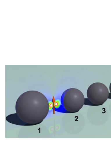
First, we consider an electric dipole source placed in a close proximity to a dielectric sphere [see Fig. 1(a)]. According to the Mie theory [14], it can be analytically shown that high permittivity dielectric nanoparticles exhibit strong magnetic resonance in the visible range when the wavelength inside the nanoparticle equals its diameter [15], where and are refractive index and radius of the nanoparticle, respectively. There are many dielectric materials with high enough real part of the permittivity and very low imaginary part, indicating low dissipative losses. To name just a few, silicon (Si, ), germanium (Ge, ), aluminum antimonide (AlSb, ), aluminum arsenide (AlAs, ), and other.
In our study we concentrate on the nanoparticles made of silicon, since it satisfies all the requirements being widely used in optics. The real part of the permittivity of the silicon is about [16], while the imaginary part is up to two orders of magnitude smaller than that of nobel metals (silver and gold). Silicon nanoparticles support strong magnetic resonance in the visible range for the radius varying from nm to nm [12].
For such a small radius compared to the wavelength , the radiation pattern of the silicon nanoparticle in the far field at the magnetic or electric resonances will resemble that of magnetic or electric point-like dipole, respectively. Moreover, it is even possible to introduce magnetic and electric polarisabilities [12, 14, 17] based on the Mie dipole scattering coefficients and : . Thus, the dielectric nanoparticle excited by the electric dipole source at the magnetic resonance may result in the total far field radiation pattern which is similar to that of the Huygens source. Similar radiation patterns can be achieve in light scattering by a magnetic particle when permeability equals permittivity [18]. Our result suggests that even a dielectric nonmagnetic nanoparticle can support two induced dipoles of equal strength resulting in suppression of the radiation in the backward direction. Thus, it can be considered as the simplest and efficient optical nanoantenna with very good directivity.
In general, both polarisabilities and are nonzero in the optical region [12]. It is known that for a dipole radiation in the far field the electric and magnetic components should oscillate in phase to have nonzero energy flow. In the near field the electric and magnetic components oscillate with phase difference, thus, the averaged Poynting vector vanishes, and a part of energy is stored in the vicinity of the source. In the intermediate region, the phase between two components varies form to 0. By placing a nanoparticle close to the dipole source will change the phase difference between two components, and, thus, affect the amount of radiation form the near field. In the case of plasmonic nanoparticles which exhibit electric polarizability only, there is an abrupt phase change from 0 to in the vicinity of the localized surface plasmon resonance, which makes it difficult to tune plasmonic nanoantennas for optimal performance. The dependence of the scattering diagram on the distance between the electric dipole source and metallic nanoparticle was studied in Ref. [19]. On contrary, in the case of nanoparticles with both electric and magnetic polarisabilities, it is possible to achieve more efficient radiation from the near to far field zone, due to subtle phase manipulation. This is exactly the case of the dielectric nanoparticles.
Any antenna is characterized by two specific properties, Directivity and Radiation Efficiency , defined as [6, 9]
| (1) |
where and are integrated radiated and absorbed powers, respectively, and are spherical angles, and is the radiated power in the given direction and/or .

The Directivity measures the power density of the antenna radiated in the direction of its strongest emission, while Radiation Efficiency measures the electrical losses that occur throughout the antenna at a given wavelength. To calculate these quantities numerically for the structures shown in Fig. 1, we employ the CST Microwave Studio. To get reliable results, we model the electric dipole source by a Discrete Port coupled to two PEC nanoparticles.
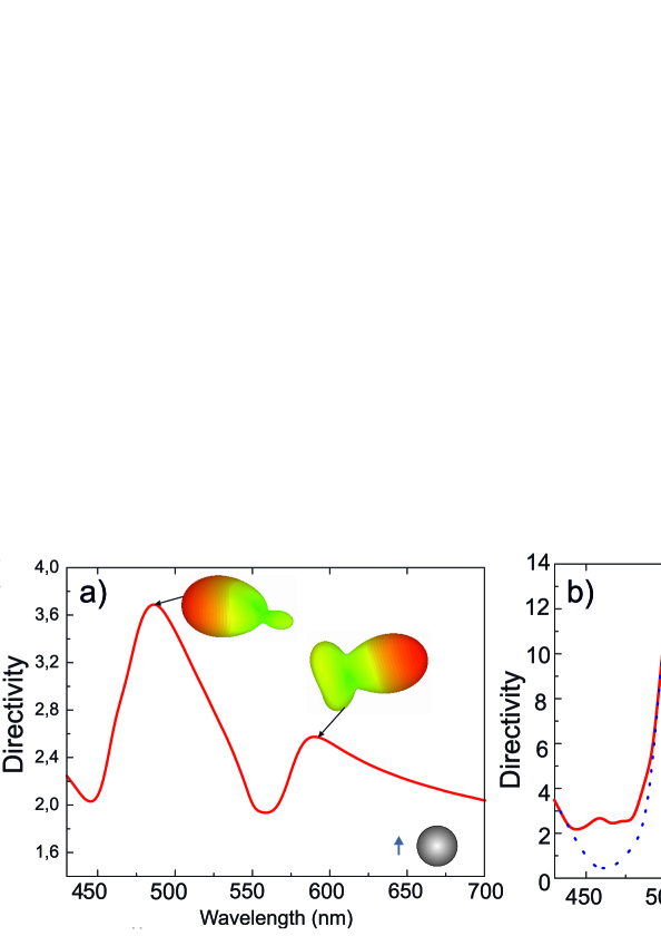
In Fig. 2(a) we show the dependence of the Directivity on wavelength for a single dielectric nanoparticle excited by a electric dipole source. Two inserts demonstrate 3D angular distribution of the radiated pattern corresponding to the local maxima. In this case, the system radiates predominantly to the forward direction at nm, while in another case, the radiation is predominantly in the backward direction at nm. In this case, the total electric dipole moment of the sphere and point-like source and the magnetic dipole moment of the sphere oscillate with the phase difference , resulting in the destructive interference in the forward direction. At the wavelength nm the total electric and magnetic dipole moments oscillate in phase and produce Huygens-source-like radiation pattern with the main lobe directed in the forward direction.
By adding more elements to the silicon nanoparticle, we can enhance the performance of all-dielectric nanoantennas. In particular, we consider a dielectric analogue of the Yagi-Uda design (see Fig.1) consisting of four directors and one reflector. The radii of the directors and the reflector are chosen to achieve the maximal constructive interference in the forward direction along the array. The optimal performance of the Yagi-Uda nanoantenna should be expected when the radii of the directors correspond to the magnetic resonance, and the radius of the reflector correspond to the electric resonance at a given frequency, with the coupling between the elements taken into account. Our particular design consists of the directors with radii nm and the reflector with the radius nm. In Fig. 2(b) we plot the directivity of all-dielectric Yagi-Uda nanoantenna vs. wavelength with the separation distance nm. Inserts demonstrate the 3D radiation patterns at particular wavelengths. We achieve a strong maximum at nm. The main lobe is extremely narrow with the beam-width about and negligible backscattering. The maximum does not correspond exactly to either magnetic or electric resonances of a single dielectric sphere, which implies the importance of the interaction between constitutive nanoparticles.

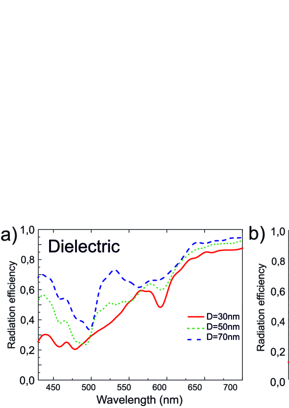
As the next step, we study the performance of the all-dielectric nanoantennas for different separation distances , and compare it with a plasmonic analogue of the similar geometric design made of silver nanoparticles. According to the results summarized in Fig. 3, the radiation efficiencies of both types of nanoantennas are nearly the same for larger separation of directors nm with the averaged value . Although dissipation losses of silicon are much smaller than those of silver, the dielectric particle absorbs the EM energy by the whole spherical volume, while the metallic particles absorb mostly at the surface. As a result, there is no big difference in the overall performance of these two types of nanoantennas for relatively large distances between the elements. However, the difference becomes very strong for smaller separations. The radiation efficiency of the all-dielectric nanoantenna is insensitive to the separation distance [see Fig. 3 (a)]. On contrary, the radiation efficiency drops significantly for metallic nanoantennas [see Fig. 3 (b)].
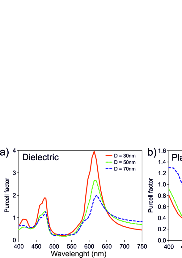
Finally, we investigate the modification of the transition rate of a quantum point-like source placed in the vicinity of dielectric particles. For electric-dipole transitions and in the weak-coupling regime, the normalised spontaneous decay rate , also known as Purcell factor, can be calculated classically as the ratio of energy dissipation rates of an electric dipole [20]. Here, and correspond to transition rate of the quantum emitter and energy dissipation rate of the electric dipole in free space [21]. In the limit of the intrinsic quantum yield of the emitter close to unity, both ratios become equal to each other , which allows us to calculate the Purcell factor in the classical regime [20]. We have calculated the Purcell factor by using both, numerical and analytical approaches. Numerically, by using the CST Microwave Studio we calculate the total radiated in the far-field and dissipated into the particles powers and take the ratio of their sum to the total power radiated by the electric dipole in free space. Analytically, we employed the generalised multiparticle Mie solution [22] adapted for the electric dipole excitation [23]. We verified that both approaches produce similar results. In Fig. 4 we show calculated Purcell factor of the all-dielectric Yagi-Uda nanoantenna vs. wavelength for various separation distances. We observe that, by decreasing the separation between the directors, the Purcell factor becomes stronger near the magnetic dipole resonance. Note here, that a plasmonic analogue of the same nanoantenna made of Ag exhibits low Purcell factor less than one, see, for example, Ref. [24]. Thus, such relatively high Purcell fcan be employed for efficient photon extraction from molecules placed near all-dielectric optical nanoantennas.
3 Conclusion
We have suggested a novel type of optical nanoantennas made of dielectric nanoparticles. Such all-dielectric nanoantennas demonstrate a number of key advantages over their metallic counterparts, including much lower dissipation losses and strong optically-induced magnetization. We have analyzed an all-dielectric analogue of the plasmonic Yagi-Uda nanoantenna consisting of an array of nanoelements, and have demonstrated very high directivity with a smaller number of directors. Moreover, lower dissipation losses and localization of the electromagnetic field inside the nanoparticles allows to reduce the distance between the adjacent elements even further, without compromising the performance.
4 Acknowledgments
The authors thank C.R. Simovski for useful discussions, and acknowledge a support from the Ministry of Education and Science in Russia and the Australian Research Council.