Semiconducting Monolayer Materials as a Tunable Platform for Excitonic Solar Cells
Abstract
The recent advent of two-dimensional monolayer materials with tunable optoelectronic properties and high carrier mobility offers renewed opportunities for efficient, ultra-thin excitonic solar cells alternative to those based on conjugated polymer and small molecule donors. Using first-principles density functional theory and many-body calculations, we demonstrate that monolayers of hexagonal BN and graphene (CBN) combined with commonly used acceptors such as PCBM fullerene or semiconducting carbon nanotubes can provide excitonic solar cells with tunable absorber gap, donor-acceptor interface band alignment, and power conversion efficiency, as well as novel device architectures. For the case of CBN-PCBM devices, we predict the limit of power conversion efficiencies to be in the % range depending on the CBN monolayer structure. Our results demonstrate the possibility of using monolayer materials in tunable, efficient, polymer-free thin-film solar cells in which unexplored exciton and carrier transport regimes are at play.
Solar cell devices converting energy radiated from the sun to electricity have developed into two main families: those based on bulk inorganic semiconductors such as Si, GaAs, CdTe, and CIGS Ginley et al. (2008), in which free charge carrier generation follows light absorption without intermediate steps,
and those based on conjugated polymers and small molecules Mayer et al. (2007); Nelson (2011) or other materials where following light absorption a complex of hole and electron carriers (exciton) is formed with a binding energy in large excess of .
The latter type, referred to as excitonic solar cell (XSC)Gregg (2005), realizes charge carrier generation by dissociating bound excitons at semiconductor heterointerfaces, owing to discontinuities across the interface in the electron affinity and ionization potential.
A typical solid state XSC 111
Our discussion here does not include dye-sensitized solar cells (DSSC), in which due to the presence of a liquid phase the carrier and exciton dynamics are different than in the solid state. For a recent review of DSSC, see M. K. Nazeeruddin et al., Solar Energy 85 (2011) 1172. employs a donor-acceptor blend of conjugated polymer or small molecule donors with high optical absorption in the visible, and fullerene derivative acceptors (e.g. , PCBM or similar fullerene molecules) Mayer et al. (2007); Wienk et al. (2003); Faist et al. (2011). In such devices, the polymer donor dominates (and limits) the key physical processes in the solar cell, including optical absorption and transport of excitons and charge carriers. In particular, exciton diffusion lengths of nm prevent the use of bilayer devices, and mobilities lower than 1 limit the thickness of bulk heterojunction devices to less than the absorption depth (typically m).
In addition, tuning the HOMO and LUMO levels of conjugated polymers is a challenging task, requiring trial and error chemical synthesis of a large number of compounds; band gaps of less than 1.5 eV are hard to achieve, and thus the absorption loss in the red part of the solar spectrum can be significant Nelson (2011). Carrier transport in conjugated molecules occurs via polarons in a regime of strong electron-phonon coupling, leading to ultrafast photoexcited carrier relaxation and consequent thermalization loss.
Despite such inherent material limitations and the related constraints they place on the device architecture, polymer and small molecule XSC technologies have progressed to impressive power conversion efficiencies, currently up to approximately 11% Hel ; Dou et al. .
Alternative XSC technologies have emerged in recent years, including efficient quantum dot based Sargent (2012) and more recently nanocarbon based XSC Bernardi et al. (2012a).
The key advantage of these novel excitonic devices is the possibility of altering the HOMO and LUMO levels, the band alignment and the optical absorption by using quantum confinement in nanomaterials rather than different chemistries as in the case of polymers and small molecules. Of great relevance is also the possibility of novel device architectures Sargent (2012), while retaining the inherent advantages of solution-based, low temperature manufacturing on flexible substrates typical of XSC.
In this context, the recent advent of two-dimensional (2D) monolayer materials with tunable optoelectronic properties and high carrier mobility e.g. monolayers of graphene Geim (2009), graphene-BN Ci et al. (2010); Bernardi et al. (2012b), Splendiani et al. (2010); Radisavljevic et al. (2011); Olsen et al. (2011), and other transition-metal oxides and dichalcogenides Ataca et al. (2012) offers renewed opportunities for thin-film XSC. Although graphene is a semimetal that can only be used in Schottky-type solar cells Miao et al. (2012), other monolayers are semiconductors with strong excitonic effects and form excellent candidates for XSC. Due to the peculiar nature of transport and electron-phonon coupling in monolayer materials Song et al. (2011); Gabor et al. (2011); Li et al. (2010), novel regimes for photovoltaic operation can be envisioned, such as hot carrier extraction, multiple exciton generation and coherent exciton transport.
Even ultra-thin devices may effectively capture sunlight due to the high optical absorption of 2D monolayers: for example, one layer of graphene absorbs 2.3% of the incident intensity in the visible Nair et al. (2008), with a van der Waals stacking thickness of only 3.3 Å in the direction normal to the layer.
Tunable optoelectronic properties can be achieved by either controlling the structure and quantum confinement within the layer, or by stacking different monolayers to create novel van der Waals structures. An example of the former strategy is the case of hybridized graphene-BN (CBN) monolayers Ci et al. (2010), whose electronic band gap, optical absorption and exciton binding energy can be varied by tuning the C domain size and shape, due to quantum confinement of excitons within the C domains.
The mobility in such CBN layers synthesized by CVD can be as high as 20 Ci et al. (2010); Bernardi et al. (2012b).
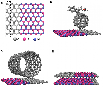
Here we show that interfaces between CBN monolayers and carbon-based acceptors such as PCBM and semiconducting single-walled carbon nanotubes (s-SWCNT) can form tunable type-II band alignments Franceschetti (2011), and are thus suitable to realize exciton dissociation in 2D monolayer based XSC. The power conversion efficiency limit resulting from such CBN interfaces is shown to be tunable, and is estimated to be in the % range. Our calculations further suggest that even just two stacked monolayers of CBN with the proper structure could constitute an ultra-thin solar cell with 3 Å thickness. We propose device architectures for the experimental study of transport, excited state dynamics and power conversion efficiency in XSC based on monolayer materials.
We employ ab initio density functional theory (DFT) calculations using the QUANTUM ESPRESSO code Giannozzi et al. (2009) on model CBN systems constituted by a monolayer with C and BN stripe domains arranged in a 2D superlattice and separated by an armchair edge. The CBN repeat unit consists of a layer with 8 atom rows and an overall composition of , where is the number of C rows in the structure, each 0.25 nm wide (Fig. 1(a)) 222
Though other geometries for C and BN domains are possible, such as quantum dots of BN in C (or viceversa), the results presented here refer to structures lacking confinement in one of the two directions within the monolayer. When confinement is introduced in both directions by forming dots (e.g. see J. Li and V. B. Shenoy, Appl. Phys. Lett. 98, 013105, 2011), the DFT band gaps are usually higher than those found here..
Interfaces containing CBN sheets (Fig. 1(b-d)) are formed by placing PCBM or s-SWCNT of chirality (10,0), (14,0), and (16,0), or a CBN layer at a Van der Waals distance of 3.3 Å from the CBN monolayer. An orthorhombic simulation cell was adopted, and all structures are fully relaxed within DFT to less than 30 meV/Å in the residual atomic forces. A 15 Å vacuum is placed in the direction normal to the sheet to avoid spurious interactions with the image system. The Perdew-Burke-Ernzerhof exchange-correlation functional Perdew et al. (1996) is adopted and ultrasoft psuedopotentials Vanderbilt (1990) are used to describe the core electrons. A kinetic energy cutoff of 35 Ry was used for the plane-wave basis set and of 200 Ry for the charge density, in combination with converged Monkhorst-Pack -point grids Monkhorst and Pack (1976) of up to . For the CBN bilayer calculations, the unit cells consisted of two layers with AB stacking in the BN domains (B atoms on top of N atoms) Liu et al. (2003), and the vdW-DF exchange-correlation functional Rydberg et al. (2003) was employed as implemented in QUANTUM ESPRESSO.
For all the interfaces studied here, the DFT derived HOMO and LUMO level offsets were estimated as differences in the peaks of the projected density of states (PDOS) for the two structures constituting the interface, similar to Ref. Kanai and Grossman (2008). Though this method is usually reliable to estimate valence band offsets Giantomassi et al. (2011), accurate conduction band offsets can only be obtained if the DFT error on the band gap is comparable for the two materials constituting the interface. In order to estimate the conduction band offsets with higher accuracy, for the CBN-PCBM interfaces we applied corrections Giantomassi et al. (2011) separately to the band gaps of both materials, and the +Bethe-Salpeter equation (+BSE) formalism to compute the optical gap of the CBN monolayers. For the CBN layers, both the corrections and the +BSE optical gaps for three compositions (, and ) were taken from our previous work Bernardi et al. (2012b). The corrections decrease linearly for increasing C domain size, so that corrections at intermediate compositions were derived by interpolation. The correction for the PCBM electronic gap was calculated here using the Yambo code Marini et al. (2009) within a update scheme, using a plasmon pole model for the dielectric function together with cutoffs of 35 Ry and 8 Ry for the exchange and correlation part of the self-energy, and up to 1500 empty bands. Further details of the many-body calculations are reported in the Supporting Material.
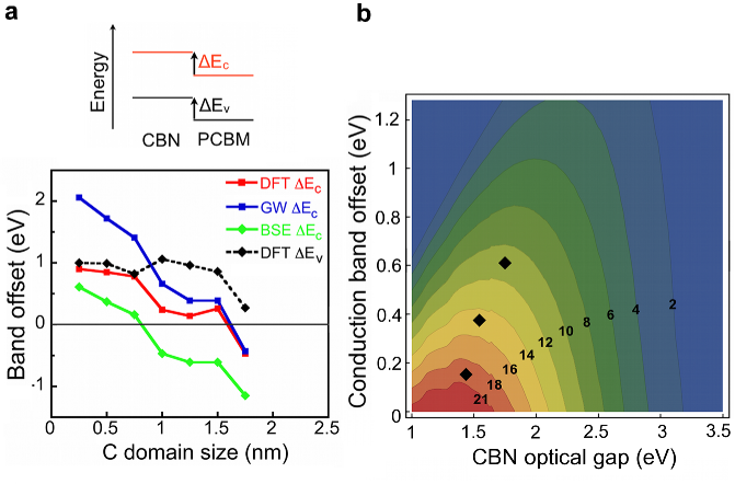
Fig. 2(a) shows the valence and conduction band offsets ( and , respectively) at different levels of theory for interfaces between PCBM and monolayers with different C domain sizes. Each consecutive point represents the addition of one C atom row in the unit cell (Fig. 1(a)), leading to a 0.25 nm increase of the C domain size. The DFT band alignment is found to be type-II for C domain sizes of up to nm, with the PCBM acting as the acceptor at the interface, as seen by the positive values of and using the convention shown in the figure. The trends in and show that the HOMO and LUMO energies of the donor can be tuned according to the C domain size, yielding unique control over the interface band offsets. This results in a tunable power conversion efficiency, as explained below.
To confirm the type-II alignment found within DFT, we apply the correction separately to the band gaps of CBN and PCBM (see Supporting Material). The corrected values 333
Note that in this work is the same at all levels of theory, since the corrections found here fall almost entirely on the LUMO level and were thus applied as a scissor correction, as further explained in the Supporting Material.
, shown in Fig. 2(a) ( curve) yield the same qualitative trends as the DFT results, with type-II alignment for C domain sizes of up to 1.5 nm.
Assuming that the CBN layer donor is also the main absorber in the XSC, the exciton binding energy in the CBN layer is the key quantity to determine the possibility to transfer a photoexcited electron to the PCBM. To address this point, we derived values as differences between the LUMO level derived from the optical gap of the CBN donor (using +BSE) and the LUMO level of the PCBM acceptor. This combined scheme utilizing the optical LUMO of the donor and the quasiparticle LUMO of the acceptor can correctly describe the minimum energy of the exciton formed after photoabsorption in the CBN donor, as well as the correct electronic quasiparticle level for the addition of the transferred electron to the acceptor. The values derived at this combined level of theory are shown in Fig. 2(a) (BSE curve), and are used below to calculate the power conversion efficiencies; within this approximation, the useful range for XSC operation is restricted to C domain sizes of up to approximately 1 nm, for which the condition is met
444Given the choice of working with superlattices instead of dots geometries, we remark that this is a lower bound of the C domain size for this effect to be observed in practice..
For the three CBN-PCBM cases satisfying this condition, we estimate a practical limit to the power conversion efficiency. The thermodynamic limit to the efficiency for thermalized carriers and in the absence of non-radiative recombination is set by the optical gap of the donor through the Schockley-Quisser limit Shockley and Queisser (1961). However, efficiency trends and practical limits are far more useful for XSC than ultimate thermodynamic limits Scharber et al. (2006); Lunt et al. (2011).
Following Scharber et al. Scharber et al. (2006), we estimate practical values of the maximum power conversion efficiency for CBN-PCBM devices with type-II alignment as:
| (1) |
where 0.65 is the fill factor (), is the AM1.5 solar energy flux (expressed in ) NRE at the photon energy , and is the optical band gap of the CBN donor.
In Eq. (1), the term is an estimate of the maximum open circuit voltage (, in eV), calculated as the effective interface gap taken between the HOMO level of the donor and the LUMO level of the acceptor, minus 0.3 eV, which accounts for energy conversion kinetics Scharber et al. (2006); Perez et al. (2009). The integral in the numerator is the short circuit current calculated using an external quantum efficiency () limit of 100%, while the denominator is the integrated AM1.5 solar energy flux, which amounts to 1000 .
The efficiency is thus estimated as the product normalized by the incident energy flux, in the limit of 100%
555
Ref. Scharber et al. (2006) uses 65% for both the and the . However, XSC with up to 75% of both values have been shown recently in the literature Lunt et al. (2011). The alternative choice of using this 75% limit for both and would lead to a decrease in the efficiency by a factor compared to the values reported here. In addition, we note that different from Ref. Scharber et al. (2006), in our work suffices to guarantee exciton dissociation at the interface, since the optical donor band gap is used instead of the electronic gap.
.
Fig. 2(b) shows the efficiency of the three CBN-PCBM interfaces with type-II alignment, as a function of the CBN donor optical gap and the interface , the latter computed as the difference between the CBN optical LUMO and the PCBM LUMO as explained above. For the , and monolayers, the efficiency values are, respectively, 11%, 15% and 20%. The striking efficiency tunability found here is achieved by changing the size of the C domain within a 1 nm range. Though such small C domains might seem challenging to achieve in practice, the immiscibility of C and BN in 2D leads to the formation of a large amount of sub-nm scale domains, to the point that the single C and BN domains cannot be resolved after the monolayer synthesis Ci et al. (2010). Strategies for controlling the domain size and shape at the atomistic scale in CBN are also being actively explored Sutter .
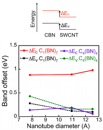
Next, we analyze the band alignment at CBN-SWCNT and CBN bilayer interfaces. Fig. 3 shows the DFT valence and conduction band offsets for interfaces between the two CBN systems and (with respectively 0.25 and 1 nm C domain size) and zig-zag s-SWCNT with three different diameters. Both and are found to be positive (with the convention shown in Fig. 3) for both CBN cases and regardless of the nanotube diameter, implying a type-II alignment for these interfaces. The band offsets show little variation with nanotube diameter, and becomes smaller for increasing C domain sizes, similar to the CBN-PCBM case. At the interface, the nanotube behaves as the acceptor, and should thus be n-doped in a real device for optimal performance.
Though we do not verify it explicitly, the type-II alignment would be retained at the and +BSE levels of theory. For the alignment type to be inverted, the correction to the nanotube band gap would need to be higher than the corresponding correction to the CBN layer band gap, which are, respectively, 3.25 eV and 1.72 eV for the and cases Bernardi et al. (2012b). However, only small corrections are predicted for s-SWCNT in this diameter range ( 10% of the band gap Miyake and Saito (2003)), and such corrections certainly cannot be as large as 1.7 eV.
Similar to the case of the CBN-PCBM interfaces, band offset values with a strong dependence on the C domain size in CBN are found, which could allow one to tune the solar cell performance by varying the structure of the CBN layer.
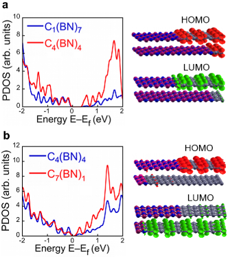
The electronic structure of bilayer systems, in which the two composing CBN monolayers have different atomic structures, is presented in Fig. 4. We show the PDOS and the HOMO and LUMO orbitals of two bilayer cases among those studied in this work. In both bilayer systems, the LUMO localizes within the layer with the smaller energy gap. For the bilayer (Fig. 4(a)), we observe a complete hybridization of the valence states, as seen by the perfect overlap of the valence PDOS, causing the HOMO to delocalize to both layers. In contrast, in the bilayer the HOMO is found to be localized on the layer, i.e. the layer with the larger band gap. In this case, the incomplete hybridization of the valence states is seen by the slight valence band offset in the PDOS. We found an analogous behavior in the system.
On this basis, we predict the interface to be a type-I heterojunction with ohmic character (due to the absence of barriers for the transport of holes), and the and interfaces to be type-II heterojunctions, in which exciton dissociation may be possible within the bilayer. In both cases, upon photoexcitation the orbitals are predicted to dramatically change their spatial distribution (Fig. 4), which may lead to opportunities for engineering the flow of photoabsorbed energy. We note that the alignment types found here for the bilayer systems are retained also beyond the DFT level of theory, since the and the +BSE corrections to the band gaps are higher for the CBN monolayer with the larger band gap Bernardi et al. (2012b).
Our results thus suggest that in principle it may be possible to fabricate a two atomic layers thick ( 3.3 Å) XSC in the form of a bilayer device, by stacking two CBN monolayers with the proper C domain structure. Alternatively, given the tunability of the CBN layer electronic structure, a Schottky junction solar cell may be formed between a monolayer of graphene and a monolayer of CBN. Considering a monolayer absorbance of approximately 2% similar to the case of graphene, a structure with as few as monolayers and a thickness of approximately 10 nm could suffice to absorb most of the incident sunlight with energy above the band gap.
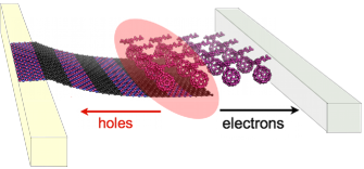
In addition to the potential technological innovation resulting from the tunability of the parameters of interest in photovoltaics, XSC based on 2D monolayer materials could constitute a new platform for the experimental study of quantum transport effects (characteristic of 2D monolayers) in photovoltaic devices. For example, while hot carrier and hot exciton transfer are possible at or near an interface Ross and Nozik (1982), in common XSC they’re hindered by the diffusion through the bulk of the absorber. However, if a solar cell is made with a single monolayer, no bulk diffusion is involved and the hot carrier regime could be enabled. In addition, the impact of coherent exciton transport on XSC performance is largely unexplored in photovoltaics, due to the fact that exciton transport operates in an incoherent regime in reasonably any m-thick bulk heterojunction solar cell fabricated using standard deposition techniques.
As a test bed for these fundamental effects, we propose in Fig. 5 an architecture whereby XSC based on 2D monolayer materials could be fabricated and characterized, for example using ultra-fast spectroscopy measurements Cabanillas-Gonzales et al. (2011) to ascertain the presence of hot exciton dissociation or hot carrier extraction.
We remark that while the tunability of the solar cell properties presented here originates from changes to the composition and domain structure of a single monolayer, additional tuning of physical quantities of interest in photovoltaics could be achieved by stacking sequences of different 2D semiconducting monolayers, an alternative approach we are currently investigating.
In summary, we present the idea of XSC based on semiconducting 2D monolayer materials with the potential to achieve % power conversion efficiencies in nm thick active layers, and show that combinations of CBN monolayers and PCBM or s-SWCNT are well-suited for the practical implementation of such devices. Even a photovoltaic device as thin as two atomic layers of CBN (with different C domain sizes, as shown here) or other monolayer materials with type-II band alignment holds the potential to achieve solar energy conversion at exceptionally small length and ultra-fast time scales. The unique tunability in 2D monolayer materials of the band gap, interface band alignment, exciton binding energy, optical absorption, carrier mobility, and electron-phonon coupling entails new opportunities for fundamental studies and practical implementation of excitonic solar cell devices.
I Acknowledgments
M.B. acknowledges funding from Intel through the Intel Ph.D. Fellowship. We wish to thank NERSC and Teragrid for providing computational resources.
II Supporting Information
Details of many-body calculations using the and BSE methods.
III References
References
- Ginley et al. (2008) D. Ginley, M. A. Green, and R. Collins, MRS Bull. 33, 355 (2008).
- Mayer et al. (2007) A. C. Mayer, S. R. Scully, B. E. Hardin, M. W. Rowell, and M. D. McGehee, Mater. Today 10, 28 (2007).
- Nelson (2011) J. Nelson, Mater. Today 14, 462 (2011).
- Gregg (2005) B. A. Gregg, MRS Bull. 30, 20 (2005).
- Note (1) Our discussion here does not include dye-sensitized solar cells (DSSC), in which due to the presence of a liquid phase the carrier and exciton dynamics are different than in the solid state. For a recent review of DSSC, see M. K. Nazeeruddin et al., Solar Energy 85 (2011) 1172.
- Wienk et al. (2003) M. M. Wienk, J. M. Kroon, W. J. H. Verhees, J. Knol, J. C. Hummelen, P. A. van Hal, and R. A. J. Janssen, Angew. Chem. Int. Ed. 42, 3371 (2003).
- Faist et al. (2011) M. A. Faist, P. E. Keivanidis, S. Foster, P. H. Wobkenberg, T. D. Anthopoulos, D. D. C. Bradley, J. Durrant, and J. Nelson, J. Polym. Sci, Part B: Polym. Phys. 49, 45 (2011).
-
(8)
The current efficiency record for small
molecule based solar cells is 10.7 % from the German company Heliatex.
See heliatex.com. - (9) L. Dou, J. You, J. Yang, C.-C. Chen, Y. He, S. Murase, T. Moriarty, K. Emery, G. Li, and Y. Yang, Nat. Photon. 6, 180 (2012). After reporting 8.6% efficient polymer tandem solar cells, the Yang’s group has realized NREL certified 10.6% efficient polymer tandem devices.
- Sargent (2012) E. H. Sargent, Nature Photon. 6, 133 (2012).
- Bernardi et al. (2012a) M. Bernardi, J. Lohrman, P. Kumar, A. Kirkeminde, N. Ferralis, J. C. Grossman, and S. Ren, Submitted. (2012a).
- Geim (2009) A. Geim, Science 323, 1530 (2009).
- Ci et al. (2010) L. Ci, L. Song, C. Jin, D. Jariwala, D. Wu, Y. Li, A. Srivastava, Z. F. Wang, K. Storr, L. Balicas, F. Liu, and P. M. Ajayan, Nature Mater. 9, 430 (2010).
- Bernardi et al. (2012b) M. Bernardi, M. Palummo, and J. C. Grossman, Phys. Rev. Lett. 108, 226805 (2012b).
- Splendiani et al. (2010) A. Splendiani, L. Sun, Y. Zhang, T. Li, J. Kim, C.-Y. Chim, G. Galli, and F. Wang, Nano Lett. 10, 1271 (2010).
- Radisavljevic et al. (2011) B. Radisavljevic, A. Radenovic, J. Brivio, V. Giacometti, and A. Kis, Nature Nanotech. 6, 147 (2011).
- Olsen et al. (2011) T. Olsen, K. W. Jacobsen, and K. S. Thygesen, e-print arXiv:1107.0600 (2011).
- Ataca et al. (2012) C. Ataca, H. Sahin, and S. Ciraci, J. Phys. Chem. C 116, 8983 (2012).
- Miao et al. (2012) X. Miao, S. Tongay, M. K. Petterson, K. Berke, A. G. Rinzler, B. R. Appleton, and A. F. Hebard, Nano Lett. (2012), dOI: 10.1021/nl204414u.
- Song et al. (2011) J. C. W. Song, M. S. Rudner, C. M. Marcus, and L. S. Levitov, Nano Lett. 11, 4688 (2011).
- Gabor et al. (2011) N. M. Gabor, J. C. W. Song, Q. Ma, N. L. Nair, T. Taychatanapat, K. Watanabe, T. Taniguchi, L. S. Levitov, and P. J. Herrero, Science 334, 648 (2011).
- Li et al. (2010) C. H. Li, K. F. Mak, J. Shan, J. Shan, and T. Heinz, Phys. Rev. Lett. 105, 127404 (2010).
- Nair et al. (2008) R. R. Nair, P. Blake, A. N. Grigorenko, K. S. Novoselov, T. J. Booth, T. Stauber, N. M. R. Peres, and A. K. Geim, Science 320, 1308 (2008).
- Franceschetti (2011) A. Franceschetti, MRS Bull. 36, 192 (2011).
- Giannozzi et al. (2009) P. Giannozzi, S. Baroni, N. Bonini, M. Calandra, R. Car, C. Cavazzoni, D. Ceresoli, G. L. Chiarotti, M. Cococcioni, I. Dabo, A. Dal Corso, S. de Gironcoli, S. Fabris, G. Fratesi, R. Gebauer, U. Gerstmann, C. Gougoussis, A. Kokalj, M. Lazzeri, L. Martin-Samos, N. Marzari, F. Mauri, R. Mazzarello, S. Paolini, A. Pasquarello, L. Paulatto, C. Sbraccia, S. Scandolo, G. Sclauzero, A. P. Seitsonen, A. Smogunov, P. Umari, and R. M. Wentzcovitch, Journal of Physics: Condensed Matter 21, 395502 (19pp) (2009).
- Note (2) Though other geometries for C and BN domains are possible, such as quantum dots of BN in C (or viceversa), the results presented here refer to structures lacking confinement in one of the two directions within the monolayer. When confinement is introduced in both directions by forming dots (e.g. see J. Li and V. B. Shenoy, Appl. Phys. Lett. 98, 013105, 2011), the DFT band gaps are usually higher than those found here.
- Perdew et al. (1996) J. Perdew, K. Burke, and M. Ernzerhof, Phys. Rev. Lett. 77, 3865 (1996).
- Vanderbilt (1990) D. Vanderbilt, Phys. Rev. B 41, 7892 (1990).
- Monkhorst and Pack (1976) H. J. Monkhorst and J. D. Pack, Phys. Rev. B 13, 5188 (1976).
- Liu et al. (2003) L. Liu, Y. P. Feng, and Z. X. Shen, (2003).
- Rydberg et al. (2003) H. Rydberg, M. Dion, N. Jacobson, E. Schroder, P. Hyldgaard, S. I. Simak, D. C. Langreth, and B. I. Lundqvist, Phys. Rev. Lett. 91, 126402 (2003).
- Kanai and Grossman (2008) Y. Kanai and J. C. Grossman, Nano Lett. 8, 908 (2008).
- Giantomassi et al. (2011) M. Giantomassi, M. Stankovski, R. Shaltaf, M. Gruning, F. Bruneval, P. Rinke, and G.-M. Rignanese, Phys. Status Solidi B 248, 275 (2011).
- Marini et al. (2009) A. Marini, C. Hogan, M. Gruning, and D. Varsano, Comp. Phys. Comm. 180, 1392 (2009).
- Note (3) Note that in this work is the same at all levels of theory, since the corrections found here fall almost entirely on the LUMO level and were thus applied as a scissor correction, as further explained in the Supporting Material.
- Note (4) Given the choice of working with superlattices instead of dots geometries, we remark that this is a lower bound of the C domain size for this effect to be observed in practice.
- Shockley and Queisser (1961) W. Shockley and H. J. Queisser, J. Appl. Phys. 32, 510 (1961).
- Scharber et al. (2006) M. C. Scharber, D. Muhlbacher, M. Koppe, P. Denk, C. Waldauf, A. J. Heeger, and C. J. Brabec, Adv. Mater. 18, 789 (2006).
- Lunt et al. (2011) R. R. Lunt, T. O. Osedach, P. R. Brown, J. A. Rowehl, and V. Bulovic, Adv. Mater. 23, 5712 (2011).
- (40) The AM1.5G spectrum was taken from the NREL website: http://rredc.nrel.gov/solar/spectra/am1.5 and integrated with the trapezoid rule.
- Perez et al. (2009) M. D. Perez, C. Borek, S. R. Forrest, and M. E. Thompson, J. Am. Chem. Soc. 131, 9281 (2009).
- Note (5) Ref. Scharber et al. (2006) uses 65% for both the and the . However, XSC with up to 75% of both values have been shown recently in the literature Lunt et al. (2011). The alternative choice of using this 75% limit for both and would lead to a decrease in the efficiency by a factor compared to the values reported here. In addition, we note that different from Ref. Scharber et al. (2006), in our work suffices to guarantee exciton dissociation at the interface, since the optical donor band gap is used instead of the electronic gap.
- (43) P. Sutter, March meeting of the American Physical Society of 2012. Abstract available at http://meetings.aps.org/link/BAPS.2012.MAR.X12.5.
- Miyake and Saito (2003) T. Miyake and S. Saito, Phys. Rev. B 68, 155424 (2003).
- Ross and Nozik (1982) R. T. Ross and A. J. Nozik, J. Appl. Phys. 53, 3813 (1982).
- Cabanillas-Gonzales et al. (2011) J. Cabanillas-Gonzales, G. Grancini, and G. Lanzani, Adv. Mater. 23, 5468 (2011).