Self-consistent Hartree theory of the role of electron-electron interactions in the electronic structure and conductance quantization of graphene nanoconstrictions
Abstract
We present self-consistent calculations of electron transport in graphene nanoconstrictions within the Hartree approximation. We consider suspended armchair ribbons with V-shaped constrictions having perfect armchair or zigzag edges as well as mesoscopically smooth but atomically stepped constrictions with cosine profiles. Our calculations are based on a tight-binding model of the graphene and account for electron-electron interactions in both the constriction and the semi-infinite leads explicitly. We find that electron interactions result in (i) Electrons accumulating along edges of the uniform ribbon and along zigzag and cosine constriction edges but not along armchair constriction edges. (ii) The first subband showing almost perfect transmittance due to localization at the uniform graphene boundary except at low energies for the cases of zigzag and cosine constrictions where Bloch stop-bands form in related periodic structures. (iii) The second subband being almost perfectly blocked by the constriction. (iv) Electron interactions favor intra-subband scattering while the non-interacting electron theory predicts predominance of inter-subband scattering. (v) Conductance quantization for the first few conductance steps being more pronounced for armchair constrictions but less so for zigzag constrictions. (vi) A much more prominent conductance plateau for the cosine constriction than is found in the absence of electron interactions. Possible implications for recent experiments are briefly discussed.
pacs:
72.10.Fk,73.23.Ad,81.05.UwI Introduction
Graphene nanoribbons are strips of graphene several nanometers wide and of arbitrary length. Their unique electronic structure and transport properties that arise from the linear, massless Dirac-like spectrum of the underlying honeycomb lattice of graphene are attracting a great deal of interest at the present time.review In experimental studies of graphene nanoribbons the electronic charge density in the ribbon is usually varied by the application of a variable voltage to a gate electrode located near the ribbon.Han07 ; Chen07 ; Lin08 ; Li08sonif ; Wang08 ; Molitor09 ; Stampfer09 ; Jiao09 ; Todd09 If, due to the application of the gate voltage, there is a net charge on the ribbon, the electronic charge density in the ribbon ceases to be uniform, and there is a strong redistribution of the charge towards the edges of the ribbon. This charge redistribution and its effects on the electronic structure and transport have been examined theoretically by several authors for ribbons of uniform width separated from the gate electrode by a dielectric film.FR07 ; Silvestrov08 ; Shylau09 ; others_ee It has been predicted that the charge redistribution results in a charge singularitySilvestrov08 at the edge of the ribbon (here is the coordinate normal to the ribbon boundary) and modification of the electron dispersion relation.Shylau09 Electron transport in graphene nanoribbons with constrictions (GNCs) is also attracting theoreticalMunozRojas06 ; MunozRojas08 ; Guimaraes12 ; constriction12 and experimentalTombros11 attention at the present time. However, the effects of charge redistribution in GNCs have not as yet been discussed in the literature. In this paper we explore this topic theoretically.
The present theory accounts for the effects of the Coulomb repulsion that gives rise to the charge redistribution within the self-consistent Hartree approximation that has been used previously to study charge redistribution in uniform ribbons.FR07 ; Silvestrov08 ; Shylau09 ; others_ee We consider infinite ribbons with armchair edges and V-shaped or cosine shaped constrictions and treat the effects of electron-electron interactions at the Hartree level throughout these entire structures. The ribbons that we consider are suspended above a dielectric layer which covers a gate electrode as in a recent experiment.Tombros11 We treat the effects of the dielectric and gate within an image charge model. We describe the charged nanoribbon by fixing the chemical potential, and obtaining a self-consistent solution where all electronic states with lower energies than the Fermi energy are filled. From this calculation we obtain the Hartree electronic energy bands and charge densities, and compute the conductance. Our model considers only -orbitals of the graphene within the tight-binding approximation. The structures studied below include more than 10000 carbon atoms inside the computational area.
We find that strong charge accumulation along the constriction boundary occurs or does not occur depending on the type of constriction that is considered. As more electron subbands become populated the lowest subbands gradually localize near the graphene boundary. We find that, in the Hartree model, electrons in the first subband of the ribbon are transmitted almost perfectly through the constriction with little intersubband scattering, except at the small Fermi energies where they can be resonantly reflected by a constiction having zizgag edges. By contrast, in the non-interacting electron model strong intersubband scattering occurs at the constriction. Depending on the type of constriction conductance quantization is predicted to be more or less pronounced in the Hartree approximation than in the non-interacting approximation, a finding that may be relevant to recent experimental observations.
II Model
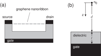
We consider a graphene nanoribbon (GN) suspended in a way similar to that in the experimental setup of Tombros etal.Tombros11 The GN is separated from the back gate by layers of a dielectric and air, see Fig. 1(a). For the dielectric material we choose SiO2 with relative permittivity . The NR is attached at its two ends to semiinfinite leads represented by ideal ribbons having the same width as the NR. Four different types of devices are considered in the following: an ideal uniform ribbon, and ribbons having V-shaped armchair and zigzag and constrictions or constrictions with cosine profiles imposed on one side. We disregard any defects other than the atomic steps at the boundary of the cosine-shaped constriction in the present study. The host configuration is taken as armchair as are the edge configurations of the semiinfinite leads.
As representative devices we consider GNs of width nm and length nm, Fig. 1(a). There are 92 carbon atoms in the cross-section making the ribbon semiconducting. The constrictions, if imposed, are V-shaped or cosine-shaped trenches 5 nm deep inside the ribbon thus leaving half of the width of the ribbon in the narrowest part of the constriction for electron propagation. The length is taken long enough to include part of the leads near the constriction and therefore to treat the leads accurately. Because for the V-shaped constrictions we consider atomically ideal boundaries, the apex angles of these constrictions are 60 and 120 degrees for armchair and zigzag cases, respectively. The SiO2 and air layers are both 50 nm thick. Thus the back gate is 100 nm from the nanoribbon. We performed simulations for different ribbon widths for these constriction geometries and all of the results showed similar features.
The system shown in Fig. 1 is described by the Hamiltonian
| (1) |
where eV is the matrix element between nearest-neighbor atoms; is the Hartree potential at atom which results from the Coulomb interaction with the uncompensated charge density in the system (including the image charges). In coordinate space the Hartree potential can be written as
| (2) |
where is the electron or image charge placed at distance from the graphene layer. The image charges included in the model keep the back-gate electrode at zero potential.Shylau09 ; Silvestrov08 ; FR07 ; Peres09 The potential due to a charge density located a distance above a dielectric (with dielectric constant and thickness ) that is over a metal gate, as shown in Fig. 1(b), can be described by an infinite number of image charge densities. The first few image charge densities and their -coordinates (measured from the position of the electron charge) and also the electron charge density itself are given in Table 1. The first row () describes the direct Coulomb interaction between electrons in the graphene layer. Because the contributions from the image charges decrease rapidly as grows and in order to facilitate computation the results presented below were obtained keeping only the terms.
| coordinate, | charge density, | |
| 0 | 0 | |
| 1 | ||
| 2 | ||
| 3 | ||
| 4 | ||
| … | … | … |
The integration in (2) was performed over the whole device including the semiinfinite leads. In order to include electron-electron interactions over the whole system, we partition the system into three parts, the internal computational region and two semi-infinite leads.qpc ; opendot The internal region incorporates not only the constriction but also segments of uniform ribbon on both sides of it, including part of the leads. The semi-infinite leads themselves begin far enough from the constriction to ensure that the total self-consistent potential and the electron density do not change appreciably along the leads, i.e., the electron density and the potential in the leads are not affected by the internal region. Thus the leads can be considered as uniform graphene ribbons.
Starting from the Hamiltonian Eq. (1), we evaluate the Green’s function numerically using the technique described by Xu et al.Xu08 . The Green’s function in the real-space representation, , provides information about the local density of states at site ,
| (3) |
where factor 2 takes account of the spin degeneracy and is the area corresponding to one carbon atom. The density of states is . The LDOS can be used to calculate the electronic density at site
| (4) |
where is Fermi energy and is the Fermi-Dirac distribution function. All the calculations reported in this paper correspond to the temperature K. A zero temperature version of Eq. 4 has been used previously in Ref. Shylau09, . In general at non-zero temperatures the lower limit of integration in Eq. 4 is . However, in the present work the LDOS is zero in a range of energies of width much larger than below the charge neutrality point and therefore Eq. 4 is a good approximation. The position of the charge neutrality point at a given Fermi energy is determined numerically from solution of the Schrodinger equation
| (5) |
with being the Hamiltonian (1) and the wave function obeying the Bloch theorem
| (6) |
where is the Bloch wave vector and is the Bloch wave function at coordinate ; is unit cell length of the armchair ribbon.Xu08 ; corrugation09 ; zigzag_localization Having calculated the Bloch states and constructed the band diagram one can readily obtain the number of the Bloch states for a given Fermi energy that in turn serves as a basis for analysis of transport properties of GNCs.corrugation09 Because the projections of the two Dirac points in the armchair ribbon coincide at we solve (5) at zero wave vector and find from eigenvalues .
The integration path in (4) goes along the real axis and a fine integration grid is used to capture the locations of the subband edges and quasibound states if any are present.
Since the Hartree potential given by Eq. (2) depends on the electron density which is a solution of the Schrödinger equation with the Hamiltonian (1), these equations need to be solved iteratively. The iteration process is executed until the convergence criterion is met, where and are the input and output average values of the electron density at the -th iteration. In the cases where a constriction is present in the GN the above computation proceeds in two stages. At the first stage, self-consistency is achieved for the uniform ribbon. Then constriction is imposed on the ribbon and self-consistency is achieved again.
Having calculated the electron density and the position of the Dirac point numerically, we are in a position to find the conductance
| (7) |
as a function of the Fermi energy. Here is the transmission coefficient from subband in the left lead to the subband in the right lead, at energy . is calculated by the recursive Green’s function method, see Ref. Xu08, for details.
The Fermi energy and charge neutrality point are related to a value of the gate voltage measured in experimental setup as .FR07 ; Shylau09 In a real device, it is the gate voltage that results in a change of carrier density in the graphene ribbon. We define as the chemical potential difference between the metallic gate and the ribbon, necessary to accommodate extra carriers in the graphene and remove them from the metallic gate. Knowledge of both and thus allows one to estimate the value of used in an experiment. Note that in the non-interacting approach.
III Results
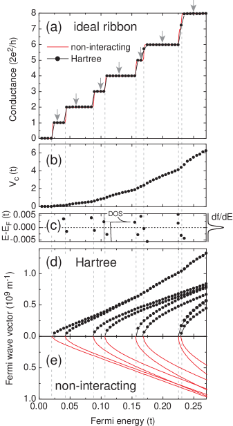
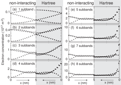
Figure 2 shows results for uniform GNs: (a) the conductance, (b) the charge neutrality point, (c) the positions of the bottoms of the subbands that are near the Fermi energy, and (d) and (e) the wavevectors at the Fermi energy calculated within the Hartree and non-interacting models, respectively. The conductance values for the two models for the same values of the Fermi energy are very close to each other. In both cases the conductance increases by the quantum each time a new subband opens for propagation. The opening of a new electron subband also results in an increase in the slope of the charge neutrality point vs. Fermi energy as is seen in Fig. 2(b); increases monotonically with increasing Fermi energy because the electron density on the ribbon increases. The slope change is caused by the additional contribution to the electrostatic potential on the ribbon due to the charges populating a new subband. Assuming a parabolic dispersion near the subband edge yields an divergence of the DOS that leads to an additional electron density where E is measured from the subband edge. The associated charge contributes to the Hartree potential that in turn leads to the rise in .
The subband energy position shown in Fig. 2(c) reveals a linear drop of the energy levels relative to as increases. Each time an energy level crosses electrons start populating the GN and contribute to the electrical conductance. Note that the bottoms of the subbands in the GN do not show any pinning to the Fermi level such as that observed in conventional quantum wiresHirose01 and open quantum dotsopendot . As can be seen in Fig. 2(d), the electron interactions modify the band structure of the GN: The results for the Hartree model show avoided crossings and the two lowest subbands having smaller velocities. The reason for these modifications of the band structure due to electron-electron interactions can be understood from the analysis of the charge distribution in the GN that is shown in Fig. 3: The electron interactions in the Hartree model result in strong redistribution of the charges towards the edges of the ribbon when the Fermi energy is increased. The larger the Fermi energy, the stronger redistribution of the electron density. Note that the charge accumulation along the boundaries of uniform graphene strips was also discussed in Refs. FR07, ; Silvestrov08, ; Shylau09, ; others_ee, .
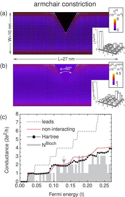
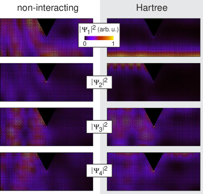
Figure 4(c) shows the conductance as a function of the Fermi energy for a GN with an armchair constriction. The non-interacting electron calculation predicts conductance quantization in steps of over the whole range of values shown in Fig. 4(c). However, the results of the Hartree calculation show only first two conductance plateaus to be well defined. The transition between these plateaus appears sharper than that predicted by the non-interacting calculation. In order to understand the reason for the better quantization for the first few conductance steps in the Hartree approach let’s inspect the electron concentration distributions and transmission coefficients for shown in Fig. 4 (a) and (b). The charge density is enhanced along the bottom straight boundary in Fig. 4 (a) and (b) in a similar way to that in the uniform GN discussed above. However the enhancement that occurs along the armchair constriction is very non-uniform: Much less charge accumulates near the apex at the narrowest part of the constriction; see Figs. 4(a) and (b), respectively, for the electron concentration distribution in the Hatree calculation and the difference between the Hartree and non-interacting electron concentrations . The partial transmission in the Hartree model reveals nearly perfect transmittance for the first state, see inset in Fig. 4(a). Note that for all of the conductance steps in the Hartree theory. However, the transmittance due to the second state was found to be strongly suppressed. for the non-interacting approach shows a fairly uniform distribution over all states, see inset in Fig. 4(b). To understand this phenomenon, let’s consider the square moduli of the wave functions shown in Fig. 5. The first state in the Hartree approach transmits nearly perfectly because of its localization near the straight bottom boundary. By contrast, the second state is mostly localized near the top boundary, where the constriction is located and transmission is therefore blocked. Note that localization develops gradually as increases and the first and second states propagating along opposite boundaries reveal very similar dispersion for the uniform ribbon for , see Fig. 2(d). These two states become mostly trapped within triangular wells at the straight ribbon boundaries. It is also worth noting that this phenomenon holds true for all of the constriction shapes studied below. It does not occur in the non-interacting electron model because of the absence of change accumulation near the boundaries. In general, we find electron interactions to favor intra-subband scattering whereas in the non-interacting approximation inter-subband scattering predominates. The conductance step degradation in the Hartree model for in Fig. 4(c) is related to the overall poor transmittance of the highest states, where the charge accumulation along the ribbon’s edges but not in the constriction itself is further increased. When this happens the constriction becomes a more effective obstacle to electron propagation through the ribbon in the Hartree theory than in the non-interacting electron approximation.
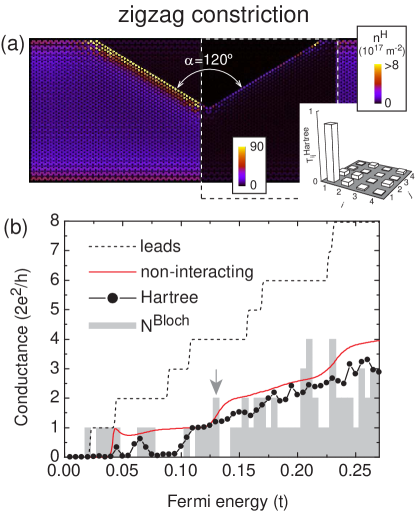
The conductance as a function of and a representative electron concentration distribution for a zigzag constriction are shown in Figures 6(b) and (a). The charge density along the zigzag constriction edge is strongly enhanced by values up to an order of magnitude larger than for the armchair constriction; see the density scales in the inset in Fig. 6(a). One reason for this is the electron localization at zigzag edges previously predicted in both non-interacting and interacting electron theories; see, for example, Refs. corrugation09, ; zigzag_localization, ; Brey06, . This is a topological property of zigzag-terminated ribbons. Another reason is the effect of electron interactions that increases the charge density along the edge further. The electrons occupy only one graphene sublattice along the zigzag edge while they occupy both sublattices along the armchair edge. We find the crossover between these charge occupations to occur over a distance of about 10 carbon atoms at the armchair-to-zigzag junction. The partial transmission for the first subband is similarly to the case of the armchair constriction although it is suppressed at and due to resonant backscattering by strongly localized states at the zigzag edge. It is worth noting that in modulated ribbons consisting of periodically repeated identical constrictions stop-bands form at these energies. These stop-bands, where the number of propagating Bloch states (the grey shading in Fig. 6(b)) in the periodic structure is zero, are similar to those predicted in edge-corrugated graphene ribbons.corrugation09 However, here the stop-bands form due to electron interactions. The mismatch between the electronic structures of the armchair host and zigzag constriction also contributes to less pronounced conductance quantization being seen in Fig. 6(b) for the zigzag constriction than in Fig. 4(c) for the armchair constriction.
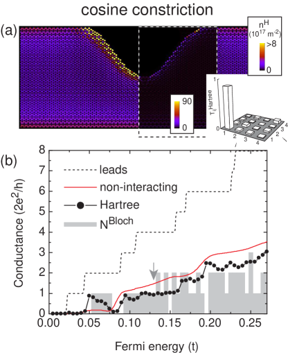
Figure 7 shows a representative electron concentration distribution and the conductance for a constriction with a cosine profile. We found strong accumulation of the charge density along the boundary of the constriction itself, similar to that for the zigzag constriction. Note that even though the overall shape of the cosine constriction is smooth there are multiple pieces of the zigzag terminated edges connected to each other by atomic steps along the constriction boundary. The conductance dip at is correlated to the absence of propagating Bloch states at this energy in the corresponding modulated ribbon with periodically repeated constrictions, as is the case for the similar features in Fig. 6(b) for the zigzag constriction. Interestingly, although in Fig. 7(b) only hints of conductance plateaus can be seen in the results for the non-interacting electron model (red solid curve), a very pronounced first conductance plateau is found when electron interactions are included in the Hartree model (dots), although only hints of higher plateaus can be discerned in this case as well. We find the first conductance plateau to remain robust for GNCs with the cosine shape of length 7-16 nm (not shown). It may be relevant that in their experimental study of a constriction with an overall smooth profile (albeit for a much larger structure than those studied here) Tombros et al.Tombros11 observed a very pronounced first integer conductance plateau but only very weak higher plateaus or only hints of higher plateaus. In such a scenario, a well defined first plateau may be caused by the lowest state being adiabatically transmitted along one of the graphene boundaries in an asymmetric constriction with curvature of one boundary being much smaller than that of the other. Because no image of the constriction on which the transport measurements were carried out was presentedTombros11 , the degree of asymmetry is not known. Note also that the experimental device in Ref. Tombros11, was fabricated by current annealing that substantially reduces edge disorder at both boundaries.
IV Summary
In conclusion, we have presented a self-consistent model of electron quantum transport in graphene ribbons and constrictions. The latter are represented as trenches of depth 5 nm and length range 7-17 nm and having different shapes. The model is based on the Green’s function formalism and accounts for electron-electron interaction within the Hartree approach. The Hartree model predicts several features not found in the non-interacting model. The electron charge density gradually accumulates along straight boundaries of uniform ribbons as the Fermi energy increases. However, accumulation at the constriction depends strongly on the details of the constriction geometry. There is little if any charge accumulation along a V-shaped armchair constriction boundary but strong accumulation along a V-shaped zigzag boundary or a boundary with an overall smooth cosine profile. For each of these constriction types imposed on a ribbon with armchair boundaries, except near isolated reflection resonances, we find almost perfect transmission of electrons in the first subband (with little inter-subband scattering) and almost perfect reflection of electrons in the second subband of the ribbon in the Hartree model. By contrast, we find the constriction to induce strong intersubband scattering of electrons for every subband in the non-interacting electron model. For the constriction with the cosine profile, the first integer conductance plateau is much more pronounced in the Hartree model than in the non-interacting model, a finding that may be relevant to the recent experiment of Tombros et al.Tombros11 . The transport properties of two lowest subbands are the result of by electron localization near the opposite boundaries of the ribbon. An analogy can be drawn between perfect transmission along a uniform graphene boundary and the edge state transport in the quantum Hall effect, where both are immune to defects in interior of a device.
Acknowledgements.
This research was supported by CIFAR, NSERC, Compute Canada and Westgrid.References
- (1) For a recent review see G. Kirczenow and S. Ihnatsenka, “Exploring Quantum Transport in Graphene Ribbons With Lattice Defects and Adsorbates,” in Graphene Nanoelectronics: Metrology, Synthesis, Properties and Applications edited by H. Raza (Springer, Berlin Heidelberg New York, 2012)
- (2) M. Y. Han, B. Özyilmaz, Y. Zhang, and P. Kim, Phys. Rev. Lett. 98, 206805 (2007);
- (3) Z. Chen, Y.-M. Lin, M. J. Rooks, Ph. Avouris, Physica E 40, 228 (2007)
- (4) Yu-Ming Lin, V. Perebeinos, Zhihong Chen, and Ph. Avouris, Phys. Rev. B 78, 161409(R) (2008)
- (5) X. Li, X. Wang, L. Zhang, S. Lee, H. Dai, Science 319, 1229 (2008)
- (6) X. Wang, Y. Ouyang, X. Li, H. Wang, J. Guo and H. Dai, Phys. Rev. Lett. 100, 206803 (2008)
- (7) F. Molitor, A. Jacobsen, C. Stampfer, J. Güttinger, T. Ihn, and K. Ensslin, Phys. Rev. B 79, 075426 (2009)
- (8) C. Stampfer, J. Güttinger, S. Hellmüller, F. Molitor, K. Ensslin, and T. Ihn, Phys. Rev. Lett. 102, 056403 (2009)
- (9) L. Jiao, L. Zhang, X. Wang, G. Diankov and H. Dai, Nature 458, 87 (2009)
- (10) K. Todd, H.-T. Chou, S. Amasha, and D. Goldhaber-Gordon, Nano Lett. 9, 416 (2009)
- (11) J. Fernández-Rossier, J. J. Palacios, L. Brey, Phys. Rev. B 75, 205441 (2007).
- (12) P. G. Silvestrov and K. B. Efetov, Phys. Rev. B 77, 155436 (2008).
- (13) A. A. Shylau, J. W. Klos, and I.V. Zozoulenko, Phys. Rev. B 80, 205402 (2009).
- (14) D. I. Odili, Y. Wu, P. A. Childs, and D. C. Herbert, J. Appl. Phys. 106, 024509 (2009); D. A. Areshkin and Branislav K. Nikolić, Phys. Rev. B 81, 155450 (2010); J. J. Palacios, J. Fernández-Rossier, L Brey and H A Fertig, Semicond. Sci. Technol. 25, 033003 (2010); A. A. Shylau, I. V. Zozoulenko, H. Xu and T. Heinzel, Phys. Rev. B 82, 121410(R) (2010); F. T. Vasko and I. V. Zozoulenko, Appl. Phys. Lett. 97, 092115 (2010); Z. Wang and R. W. Scharstein, Chem. Phys. Lett. 489, 229 (2010); M. V. Medvedyeva and Ya. M. Blanter, Phys. Rev. B 83, 045426 (2011) A. A. Shylau and I. V. Zozoulenko, Phys. Rev. B 84, 075407 (2011).
- (15) F. Muñoz-Rojas, D. Jacob, J. Fernández-Rossier and J. J. Palacios, Phys. Rev. B 74, 195417 (2006).
- (16) F. Muñoz-Rojas, J. Fernández-Rossier, L. Brey and J. J. Palacios, Phys. Rev. B 77, 045301 (2008).
- (17) M. H. D. Guimarães, O. Shevtsov, X. Waintal and B. J. van Wees, Phys. Rev. B 85, 075424 (2012).
- (18) S. Ihnatsenka and G. Kirczenow, Phys. Rev. B 85, 121407(R) (2012).
- (19) N. Tombros, A. Veligura, J. Junesch, M. H. D. Guimaraes, I. J. Vera-Marun, H. T. Jonkman and B. J. van Wees, Nature Physics 7, 697 (2011).
- (20) N. M. R. Peres, J. N. B. Rodrigues, T. Stauber and J. M. B. Lopes dos Santos, J. Phys.: Condens. Matter 21, 344202 (2009).
- (21) S. Ihnatsenka and I.V. Zozoulenko, Phys. Rev. B 76, 045338 (2007).
- (22) S. Ihnatsenka, I. V. Zozoulenko, and M. Willander, Phys. Rev. B 75, 235307 (2007).
- (23) H. Xu, T. Heinzel, M. Evaldsson, and I. V. Zozoulenko, Phys. Rev. B 77, 245401 (2008).
- (24) S. Ihnatsenka, I. V. Zozoulenko and G. Kirczenow, Phys. Rev. B 80, 155415 (2009).
- (25) K. Nakada, M. Fujita, G. Dresselhaus and M. S. Dresselhaus, Phys. Rev. B 54, 17954 (1996).
- (26) L. Brey and H. A. Fertig, Phys. Rev. B 73, 235411 (2006).
- (27) K. Hirose, S.-S. Li, and N. S. Wingreen, Phys. Rev. B 63, 033315 (2001).