Elastic transport through dangling-bond silicon wires on H passivated Si(100)
Abstract
We evaluate the electron transmission through a dangling-bond wire on Si(100)-H (2). Finite wires are modelled by decoupling semi-infinite Si electrodes from the dangling-bond wire with passivating H atoms. The calculations are performed using density functional theory in a non-periodic geometry along the conduction direction. We also use Wannier functions to analyze our results and to build an effective tight-binding Hamiltonian that gives us enhanced insight in the electron scattering processes. We evaluate the transmission to the different solutions that are possible for the dangling-bond wires: Jahn-Teller distorted ones, as well as antiferromagnetic and ferromagnetic ones. The discretization of the electronic structure of the wires due to their finite size leads to interesting transmission properties that are fingerprints of the wire nature.
pacs:
73.63.Nm,73.20.-r,75.70.-iI Introduction
The development of information technology has been pursued at a tremendous pace. Larger capacity memories and faster processors are obtained from the miniaturization of electronic devices. Nevertheless, this technological explosion that started in the second half of the 20th century will reach a limit when facing the nanometer scale. Indeed, at this size, the bulk properties of semiconductors are not accessible any more. Thus, the operating principles will vanish along their miniaturisation process. muller1999a ; meindl2001a In the mid-1970s, an alternative was proposed that single molecules could perform the same basic functions of electronics devices that are traditionaly silicon-based fabricated. aviram1974a ; joachim2000a For this purpose, organic molecules are candidates with great potential given the control on molecular design rending possible by chemical synthesis. In particular, one can conceive and experiment on single molecules that switch from one state to another under the application of some external stimulus kahn1988a or even amplify a signal. joachim2000a Binary data can also be encoded in a single molecule to build up complex circuit. Then, logic operations, either basic (AND, NOT, OR) or more elaborated can be performed at the molecular level, giving rise to molecular logic gates. raymo2002a ; liu2010a ; puntoriero2011a ; renaud2011b
One interesting problem is to design the atomic scale circuit where a number of these molecular logic gates will be (i) assessed and (ii) interconnected to obtain more complex circuits. Well designed atomic scale circuits can also perform logic functions by themselves without the need of molecular logic gates. kawai2012a It has been shown that such atomic scale structures can be constructed using the scanning tunneling microscope (STM). It can for example selectively remove H atoms on the surface of H-passivated semiconductors to construct dangling bonds (DBs)lines. shen1995a ; hosaka1995a ; hitosugi1999a ; soukiassian2003a ; hallam2007a ; haider2009a ; pitters2011a Those DBs are introducing electronic states in the surface band gap of the passivated semiconductor surface. An important example of such construction is the DB wire produced by the selective removal of hydrogen atoms from an H-passivated Si(001) surface along the Si dimer row (see Fig. 1). This DB wire has a single dangling bond per Si atom, intuitively offering a 1D metallic band within the gap. The transport electronic properties of such a wire has been previously inspected by Extended Hückel calculations and explained using a tight-binding model. doumergue1999a ; kawai2010a Unfortunately, the later configuration is not stable and a Peierls distortion takes place, involving a metal-insulator transition. The unstable DB wire, referred to as the ideal wire in the following, can also relax in two magnetic forms resulting from the antiferromagnetic and ferromagnetic coupling of adjacent DBs, respectively. The description of these different states has been the subject of intense activity thanks to density functional theory (DFT) based calculations. watanabe1996a ; watanabe1997a ; cho2002a ; bird2003 ; cakmak2003a ; lee2008a ; lee2009a ; lee2011a ; nous2011a In particular, when dealing with finite-size wires, the magnetic solutions appear to be more stable than the distorted surface structure, referred to as the non-magnetic (NM) wire. bird2003 ; lee2009a ; nous2011a Although these relaxed periodic structures break the metallicity of the DB wire by opening a gap, it does not dispose of the possibility to find a pseudo ballistic or a tunnel transport regime through a finite length DB wire.
In the present work we inspect the transport properties of finite-size DB wires (ideal, NM, AFM and FM) using the non-equilibrium Green’s Function (NEGF) approach combined with ab initio DFT. In order to complete the first model proposed by Kawai et al., kawai2010a this study is preceded by a thorough analysis of the infinite ideal wire by means of DFT-based calculations and Maximally Localized Wannier Functions (MLWFs). marzari1997a
II Computational Details
First-principles calculations are based on density functional theory (DFT) as implemented in Siesta. soler2002a ; artacho2008a Calculations have been carried out with the GGA functional in the PBE form, perdew1996a Troullier-Martins pseudopotentials, troullier1991a and a basis set of finite-range numerical pseudoatomic orbitals for the valence wave functions. artacho1999a Structures have been relaxed using a double- polarized basis sets, artacho1999a while the conductance has been computed from first-principles, using a single- polarized basis set, by means of the TranSiesta method, brandbyge2002a within the non-equilibrium Green’s function (NEGF) formalism. In all cases, an energy cutoff of 200 Ry for real-space mesh size has been used.
In order to reach a better understanding of the transport properties of the DB silicon wires, subsequent transformation of the Kohn-Sham orbitals to Maximally Localized Wannier Functions (MLWFs) marzari1997a has been applied. This scheme allows one to obtain a localized orthogonal basis sets. As a consequence MLWFs offer an extremely convenient way to translate the problem in terms of an orthogonal tight-binding approach. Plus, an ab initio evaluation of the on-site energies and hopping integrals becomes available. The numerical calculations of MLWF have been run with the Wannier90 code, mostofi2008a used as a post-processing tool of Siesta. The interface between both codes has been developed earlier by R. Korytár et al.. korytar2010a ; korytar2011a
III Ideal wire and H-junctions
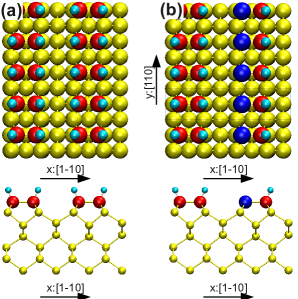
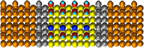
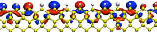
The fully hydrogenated Si(100) surface presents a (2x1) reconstruction with dimer rows formed along the (i.e. [110]) direction (see Fig. 1 (a)). Starting from this fully passivated surface, one can construct a DB wire by removing H atoms along the dimer rows direction (see Fig. 1 (b)). Before its relaxation, this DB wire presents a metallic character. Although this ideal DB wire relaxes in either a distorted wire (NM wire) or a magnetic phase (AFM and FM wires), the understanding of its electronic transmission properties remains a capital point as other cases will be regarded with respect to this reference.
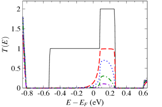
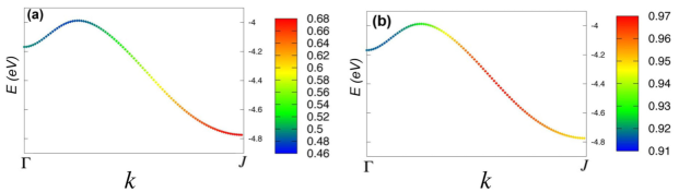
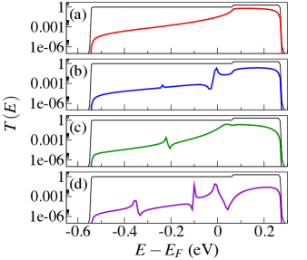
Figure 2 shows the transmission of an infinite ideal wire. As expected from its band structure, the transmission exhibits clear steps featuring the existence of two channels between 0.08 eV and 0.26 eV above the Fermi energy (), with only one remaining channel for taken between and eV. This result slightly differs from the one previously obtained by Kawai et al. kawai2010a from Extended Hückel calculations, where the energy range of the one-channel location is as large as the two-channel one ( eV), the total no zero transmission in the surface gap being the same in both calculations.
The intuitive picture is that a transmission through such these non-relaxed DB wire arises from the direct through space coupling between DBs. However, the substrate is thought to play an important role in the transport, kawai2010a and a convenient way to get rid of the direct coupling is to insert an H-passivated dimer in between two semi-infinite ideal DB wires (see Fig. 3). This peculiar structure will be considered in section V to get a better understanding of the transport and scattering mechanisms in these systems. More passivated dimers can be added in between the two ideal DB wires to track the tunnel decay through such an atomic scale surface tunnel junction.
The transmission through different length H-junctions is presented Figure 2. In the case of H-junctions longer than one passivated dimer, a tunneling regime is observed in the middle of the gap with a transmission decreasing exponentially with the length of the H-junction. For a chosen energy, the transmission can be described as:
where is the distance between semi-infinite ideal DB wires in angstrom and the inverse tunnel decay length (Å-1). At the Fermi energy, the inverse decay length is found to be Å-1 ; a value comparable to the one 0.22 Å-1 calculated with the Extended Hückel semi-empirical approximation. kawai2010a
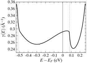
can be monitored with respect to the energy (see Fig. 4). It lies between 0.24 and 0.37 Å-1, and exhibits two local minima (maxima for the decay length Fig. 4 curve) corresponding each to the center of the one channel and two channels energy range of the ideal DB wire transmission spectrum (see Fig. 2).
The situation is qualitatively different for a single H-passivated dimer inserted between the semi-infinite wires. Indeed, this specific junction removes only one of the channels and does not affect the second channel (active between 0.08 and 0.26 eV).
At this point, the ab initio DFT-treatment, although powerful, is too global to give a clear picture of the transport mechanism through surface DB wires and H-junctions. In this regard, the parametrized tight-binding method constitutes an elegant way to model the physics of transport. Thus, one would like to take the best of both worlds and associate the accuracy of DFT-based calculations with the clarity of a simple tight-binding basis set. This is made possible by the use of Wannier functions, which allows one to (i) identify the main couplings, (ii) extract ab initio evaluations of on-site energies and hoping integrals, and (iii) use them in a tight-binding calculation.
IV Wannier functions’ analysis
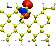
There is a large freedom in the choice of the Wannier functions used to describe the DB wire, in the sense that they are built to describe a certain energy interval of the band structure of the DB wire, and, also, the points in space around which they will be localized have to be specified as an input for the algorithm. In a first step, we choose to assign one MLWF at each bond and one function per DB along the wire. The chosen energy interval was eV. A subset of the MLWFs obtained for the ideal DB wire is depicted on Figure 5.
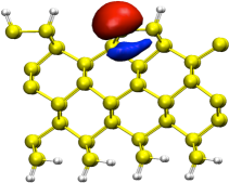
With the corresponding Hamiltonian (written in this MLWF basis set), we can study the main electronic couplings in order to rationalize the electronic properties of the DB wire. One important feature is that the direct through space electronic coupling between nearest neighbour DBs is extremely low: eV, as compared to the coupling between a DB and its subsurface functions that can reach eV. Hence, one cannot think of transport as occurring only through direct hoping between DBs since the substrate dominates transport along the wire.
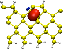
From these functions, one can interpolate the band structure. The agreement with the ab initio DFT-based band structure is excellent. As for the transport properties, we are mainly interested in the metallic band that appears at the Fermi energy resulting from the presence of the DBs. Projections of the metallic band on different sets of MLWFs are depicted in Figure 6. Here, the metallic band is correctly described when including a large set of subsurface basis functions. This indicates that the price to pay for using bond-like orbitals is that a larger number of them is required in order to properly model the transport properties of non relaxed DBs chain, i.e. to describe the metallic band accurately.
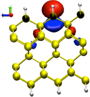
Alternatively, one can obtain a 1D tight-binding description of the system using only one basis function by considering the MLWF using only the metallic band. This leads to the calculation of an ‘effective’ orbital (see Fig. 7) that is also delocalized over the substrate.
The metallic band can then be computed from the MLWF Hamiltonian, improving the calculations by including couplings to 2, 3 or more neighbors. We found that the coupling with the fifth neighbor had to be included in the calculation in order to obtain a quantitative agreement with the DFT-based result. In the next section, the model based on this description of the wire will provide an interpretation of the scattering of electrons on a single H-junction.
V Modeling the scattering on a single H-junction
As presented earlier (see Fig. 2), the single H-junction has a transmission of in the energy window where it used to be without any H atom. Furthermore, it quickly drops to values close to zero for lower energies. To model the presence of a saturated DB which acts as a scattering center, the scattering states paulsson2007a ; frederiksen2007a will be studied where the asymptotic states are the Bloch states of a periodic DB wire. We will compare the ab initio transmission eigenchannels with the solutions found when modeling the DB wire as a one-dimensional chain with one orbital per DB site.
We start by characterizing the available asymptotic (Bloch) states at each energy. The Figure 8 shows the band structure with the corresponding right and left-going states. They are labeled channel 1 and 2 respectively in the following. It can be seen that depending on the energy window, there are two or just one channel. When visualizing these states, the change of the phase for the effective orbital, at each site, is determined by the corresponding value of the channel.
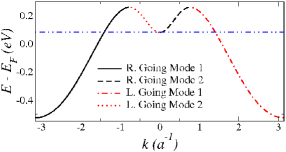
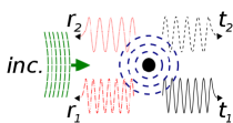
We move on now to the scattering states. For ideal wires without any scattering center, the scattering states will correspond to the Bloch states at each energy (see Fig. 9). Both channels 1 and 2 show the expected phase modulation corresponding to vectors with values of and (where is the distance between two DBs).
In the presence of an H atom (saturated DB), the incoming states will be scattered as shown in Figure 10. For energies values with just one channel and for a left incoming state, the resulting scattering state will be a superposition of the incoming wave (characterized by a certain ) and the reflected wave (with ) weighed by the (complex) coefficient ; and, to the right of the scatterer, the transmitted wave will have , and will be weighed by the transmission coefficient . As an example, in the case of the scattering state at (see Fig. 9 (c)), for a right-going state coming from the left, and . It can be seen that the transmitted wave corresponds to an outgoing wave with an associated . Since the transmission is low, with , the imaginary parts of the incoming and reflected waves cancel, leaving only the real parts of the amplitudes.
The visualization process gets more complicated in the energy window where there are two channels, since now the scattering can couple the two channels (see Fig. 10). Although the transmission and reflection coefficients could be explicitly obtained from first-principles, we can now use the one-dimensional character of the problem and model the system as a one dimensional chain, as explained above, using the parameters extracted from the MLWF transformation. This strategy allows us to: (i) explicitly obtain the transmission and reflection coefficients and hence the total transmission coefficient T(E) (that depends also on the group velocities); (ii) obtain the transmission function in less than a second – instead of hours, the typical time it takes to obtain the T(E) from first-principles for the geometries considered here. This latter aspect is particularly important if one wants to model more complex arrangements involving more than one saturated DB in extended tunnel H-junctions.
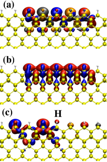
The saturated DB is modeled as a defect, in the sense that, at the saturated site, there is no available orbital for the electrons to be transfered through, as depicted in Figure 11. Different strategies can be used in order to solve the transport problem. Here we have used the Multiband Quantum Transmitting Boundary Method, proposed by Liang et al. liang1998a
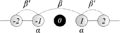
When modeling the changes in the tight-binding matrix elements due to the presence of the H atom, one can expect that the most affected matrix elements are the electronic couplings between the two DBs separated by the saturated DB, in the sense of having their effective through bond interaction reduced. Figure 11 shows a scheme of the one-dimensional model chain with one saturated DB (sites 1 and -1 are separated by a saturated DB). The matrix elements indicated in Fig. 11, are obtained from a MLWF treatment similar to the one applied on an ideal DB wire, and given in Table 1. The corresponding transmission curve is computed and shows an excellent agreement with the ab initio result. Also, for the energy window where there are two channels, the decomposition of the transmission function in terms of the contribution of the scattering of each channel into each other shows that they tend to be equally scattered.
The effect of the passivation of one DB is then to create a scattering defect that effectively mixes the two incoming Bloch waves of different values. This first inspection of the scattering properties leaves us with a physical picture for the electronic transport in these systems. Bloch waves made up by the effective orbital, that are scattered by a saturated DB as a defect in a linear chain. Due the long range electronic interactions through the substrate, this one-dimensional chain has a somehow unusual band structure, such that there can be two channels for certain energies that correspond to two Bloch states associated to two different values. This degeneracy gives rise to interesting scattering properties.
| Chain type | |||
|---|---|---|---|
| ideal | -0.053 | -4.333 | 0.190 |
| 1H | -0.041 | -4.298 | 0.182 |
VI Dangling-bond wires
As previously stated, an ideal finite DB wire is relaxing by performing either a Jahn-Teller distortion (the NM wire) or a spin polarization with the DBs coupled ferro- or antiferromagnetically (FM and AFM wires). The structures and the energetics of these different atomic surface structures have been previously described. lee2009a ; nous2011a In the case of short DB-wires, the AFM state is the most stable. But the calculated energy difference with other solutions remains too small to ignore them. lee2009a ; nous2011a Therefore, in this section, the transport properties of the three NM, AFM and NM DB wires configurations are discussed.
The system is divided into left and a right leads and a central scattering region, in our case the different possible wires (Ideal, NM, AFM and FM). brandbyge2002a ; datta_book The self-consistent density matrix is converged in the scattering region, using the open boundary conditions imposed by the leads through their self energies, using the now standard Green’s functions-based method. brandbyge2002a In order to avoid the sensitive problem of the description of the interface between realistic electrodes and the DB-wires, we choose to take advantage of the metallic behavior of the ideal wire (see section III) and use them as the source for electrons to be transferred through the scattering region. Thus, in our calculations, the role of right and left leads are performed by semi-infinite ideal wires.
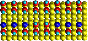
Notice that the central scattering region include (i) a finite DB-wire with a length going from 2 to 5 DBs and (ii) two H-passivated dimers placed at each end of this DB wire (see Fig. 12). Those H-junctions are used here to decouple the central DB wire from the leads. As a result, one can converge the different solutions corresponding to the different states of the DB-wire, while the leads remain as ideal DB wires.
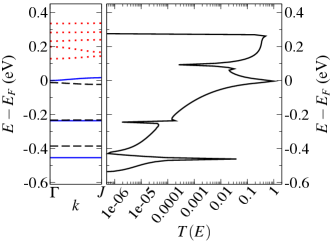
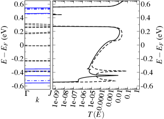
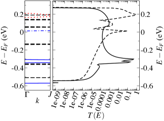
As one can then expect, the effect of the two H-passivated dimers is to lead to a confinement of the DB-wire states, thus a particle in a box-like behavior. If instead of using the open boundary conditions, one uses periodic conditions, these confined states will appear as essentially flat bands within the bulk gap as can be seen on Figure 13 on the example of a 5 DB ideal wire (blue solid lines). The corresponding transmission exhibits peaks and dips that can be understood by examining the confined states.
The three first states of an ideal 5-DB wire give clear resonance peaks in the transmission spectrum. They are within the energy range of the one-channel energy range of the ideal DB wire lead, i.e. for ( eV eV). On the other hand, the states located in the two-channel energy range result from a mixing between the states of the DB wire and the ones from the leads. As a result, the transmission spectrum does not display resonance peaks but an overall enhancement in the high energy range of the two-channel band.
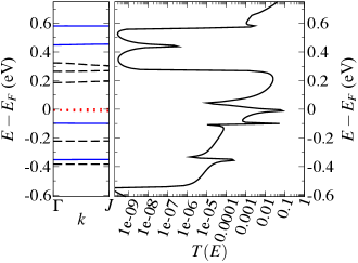
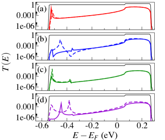
The T(E) spectral behavior is similar for a NM wire (see Fig. 14). In the case a 5-DB NM wire, the DB wire’s states give also rise to T(E) resonances. The larger transmission is obtained for a DB-wire state coupled with a state of the leads (see Fig. 15). In the two-channel energy range, the T(E) spectrum is the one observed in the case of H-junctions (see Fig. 2). Indeed, as opposed to the 5-DB ideal wire, the transmission is not perturbed by wire’s states that are shifted and give resonance peaks at higher energies. When going from a 2 to a 5-DB NM wire, the overall shape of the transmission
spectrum remains the same but with a larger number of resonance peaks corresponding to an increasing number of DB in the wire (see Fig. 16). 111Let us note that some resonance peaks are pushed outside of the energy range defined by the leads and, thus, do not show up on Figure 16 T(E) spectra.
In the same manner, the transmission through a 5-DB AFM wire exhibits resonances corresponding to states localized within the wire (see Fig. 17). Nevertheless, these states are confined below eV and above 0.3 eV, leaving the transmission largely undisturbed. The situation is the same whatever the length of the wire (see Fig. 18).
Let us stress that the difference between the transmission of both spins states in the case of odd finite length DB wires is due to the monoreferencial nature of the DFT approach that cannot deliver proper spin states. We observe an exponential decay of the transmission away from the resonances. Thus, one can define and evaluate, as in the H-junction case, an inverse decay length for the AFM wire. The calculated value Å-1 at eV is over three times larger than the one of the H-junctions at the same energy.
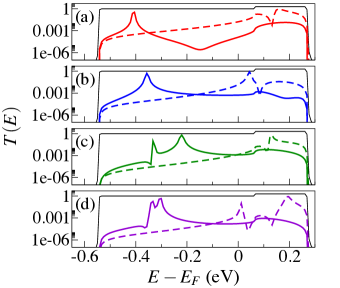
The case of the 5-DB FM wire is extremely similar to the previous one (see Fig. 19). The main difference lies in the energy distribution of the DB wire’s states depending on their spin. Indeed, as expected, the majority spin states occupy a lower range of energy, whereas the minority spin states are found near the two-channel energy range. As a consequence, the transmission spectra are extremely different for both spins, whatever the length of the finite central DB wire (see Fig. 20). The energy localization of the resonances is proper to the spin, featuring a spin filter behavior.
This systematic inspection reveals a common feature in the transmission of finite size DB wires due to an overall general behavior of . It is due to the original shape of the ideal DB wire, used here as electrode. This smooth transmission function is then perturbed by multiple resonances arising from states of the wire confined in between passivated dimers. The positions of these peaks and dips is specific to the nature of the wire as we have just seen.
Figures 16, 18 and 20 show the electron transmission coming from an ideal DB wire, transmitting into another ideal DB wire at a given electron energy . As such, it is not easy to deduce the actual electron current in the studied systems. We have then computed the electron current using the Landauer-Büttiker formula: datta_book
| (1) |
Where, is the transmission function for an electron of energy when the bias between the two DB electrodes is , and () is the right- (left-) electrode Fermi occupation function. We further simplify the current calculation using the zero-bias tansmissions of Fig. 16, 18 and 20.
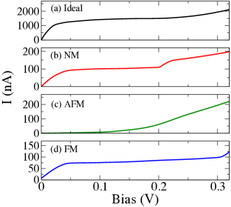
Figure 21 shows the computed I-V curves for 5-DB wires in the ideal, NM, AFM and FM configuration. As we can see, the electronic currents of actual physical wires are very reduced as compared to the current of the ideally undistorted non-magnetic wire.
Our recent study of total energy and stability of DB wires nous2011a shows that the AFM and NM solutions are thermodynamically coexisting, however their very different I-V characteristics would permit to identify the type of obtained DB wire.
VII Polaronic effects in transport
The above study only considers elastic transport. However, the large electron-vibration coupling leading the DB wires to Jahn-Teller distortions would modify transport from our above description. Indeed, a DFT-based tight-binding study suggested that transport in infinite DB wires would take place in the form of small-polaron diffusion. bowler2001a ; todorovic2002a Hole polarons are extended over 3-DB sites, bowler2001a while electron polarons present a similar confinement. bowler2001a We have estimated the extension of the induced electron polaron, by including an extra charge in the NM 5-DB wire. The most noticeable effect is that the distortion reverts sign: DB sites moving away from the surface when before they were moving against the surface and viceversa. But the degree of distortion remains the same. More importantly, the electron is not localized to only three sites, but it extends over the full wire, giving rise to no confinement except for the finite size of the DB wire. Hence, the existence of small polarons may be due to the actual extension of the DB wire implying that transport will take place by polaron hopping only in long wires. todorovic2002a
The study of the electronic ground state of the negatively charged 5-DB wire further shows that there is little difference in the electronic states of the neutral and charged wires. Indeed, one can recover the other wire’s electronic structure just by shifting the Fermi level. In this way, the new Highest Occupied Molecular Orbital (HOMO) is basically the former Lowest Unoccupied Molecular Orbital (LUMO) of the neutral 5-DB wire. Therefore, despite the need of including electron-vibration coupling in the quantitative description of DB wire transport, futuro our present results are qualitative transport descriptions because the electonic current is largely tunneled via electronic states closely resembling the neutral DB-wire states.
VIII Conclusion
In this study, we investigated the electronic transport properties of dangling-bond (DB) silicon wires on H passivated Si(100). Thanks to DFT calculations and its analysis by maximally localized Wannier functions, we have been able to rationalize the transport properties of these DB wires. As an example, we have shown the effect of a Hydrogen impurity as a source of electron scattering in the wire. This study shows that transport mainly proceeds via subsurface atoms because the direct DB interaction is negligible. A Hydrogen impurity is then efficient in interrupting the subsurface transport because it decouples the subsurface states from the surrounding DB. In this way, a Hydrogen impurity mixes and scatters the channels of the otherwise unperturbed wire.
Different finite-size dangling-bond wires have been studied. We have considered unperturbed, Jahn-Teller distorted, antiferromagnetic and ferromagnetic wires containing 2, 3, 4 and 5 DB’s. Each wire displays typical and unique trends in the transmission, allowing us to characterize the nature of the wire from its transport properties. The size of the studied wires are in the order of the small-polaron extension of DB wires, bowler2001a producing a shifting of the electronic structure but qualitative similar features. Hence, we expect polaronic effects mainly to be important in long wires. The transport properties revealed in this study will permit to characterize the DB wires experimentally accessible. hitosugi1999a
Acknowledgments
This work has been supported by the European Union Integrated Project AtMol (http://www.atmol.eu). We acknowledge CESGA for computational resources. The authors thank F. Ortmann for fruitful discussions.
References
- (1) D. A. Muller, T. Sorsch, S. Moccio, F. H. Baumann, K. Evans-Lutterodt, and G. Timp, Nature 399, 758 (1999)
- (2) J. D. Meindl, Q. Chen, and J. A. Davis, Science 293, 2044 (2001)
- (3) A. Aviram and M. A. Ratner, Chem. Phys. Lett. 29, 277 (1974)
- (4) C. Joachim, J. K. Gimzewski, and A. Aviram, Nature 408, 541 (2000)
- (5) O. Kahn and J. P. Launay, Chemtronics 3, 140 (1988)
- (6) F. M. Raymo, Adv. Mater. 14, 401 (2002)
- (7) Y. Liu, A. Offenhäusser, and D. Mayer, Angew. Chem. Int. Ed. 49, 2595 (2010)
- (8) F. Puntoriero, F. Nastasi, T. Bura, R. Ziessel, S. Campagna, and A. Giannetto, New J. Chem. 35, 948 (2011)
- (9) N. Renaud, M. Hliwa, and C. Joachim, Phys. Chem. Chem. Phys. 13, 14404 (2011)
- (10) H. Kawai, F. Ample, Q. Wang, Y. K. Yeo, M. Saeys, and C. Joachim, J. Phys.: Condens. Matter 24, 095011 (2012)
- (11) T.-C. Shen, C. Wang, G. C. Abeln, J. R. Tucker, J. W. Lyding, P. Avouris, and R. E. Walkup, Science 268, 1590 (1995)
- (12) S. Hosaka, S. Hosoki, T. Hasegawa, H. Koyanagi, T. Shintani, and M. Miyamoto, J. Vac. Sci. Technol. B 13, 2813 (1995)
- (13) T. Hitosugi, S. Heike, T. Onogi, T. Hashizume, S. Watanabe, Z.-Q. Li, K. Ohno, Y. Kawazoe, T. Hasegawa, and K. Kitazawa, Phys. Rev. Lett. 82, 4034 (1999)
- (14) L. Soukiassian, A. J. Mayne, M. Carbone, and G. Dujardin, Surf. Sci. 528, 121 (2003)
- (15) T. Hallam, T. C. G. Reusch, L. Oberbeck, N. J. Curson, and M. Y. Simmons, J. Appl. Phys. 101, 034305 (2007)
- (16) M. B. Haider, J. L. Pitters, G. A. DiLabio, L. Livadaru, J. Y. Mutus, and R. A. Wolkow, Phys. Rev. Lett. 102, 046805 (2009)
- (17) J. L. Pitters, L. Livadaru, M. B. Haider, and R. A. Wolkow, J. Chem. Phys. 134, 064712 (2011)
- (18) P. Doumergue, L. Pizzagalli, C. Joachim, A. Altibelli, and A. Baratoff, Phys. Rev. B 59, 15910 (1999)
- (19) H. Kawai, Y. K. Yeo, M. Saeys, and C. Joachim, Phys. Rev. B 81, 195316 (2010)
- (20) S. Watanabe, Y. A. Ono, T. Hashizume, and Y. Wada, Phys. Rev. B 54, R17308 (1996)
- (21) S. Watanabe, Y. A. Ono, T. Hashizume, and Y. Wada, Surf. Sci. 386, 340 (1997)
- (22) J.-H. Cho and L. Kleinman, Phys. Rev. B 66, 235405 (2002)
- (23) C. F. Bird and D. R. Bowler, Surf. Sci. 531, L351 (2003)
- (24) M. Çakmak and G. P. Srivastava, Surf. Sci. 532-535, 556 (2003)
- (25) J. Y. Lee, J.-H. Choi, and J.-H. Cho, Phys. Rev. B 78, 081303 (2008)
- (26) J. Y. Lee, J.-H. Cho, and Z. Zhang, Phys. Rev. B 80, 155329 (2009)
- (27) J.-H. Lee and J.-H. Cho, Surf. Sci. 605, L13 (2011)
- (28) R. Robles, M. Kepenekian, S. Monturet, C. Joachim, and N. Lorente, ArXiv:1203.2548v1
- (29) N. Marzari and D. Vanderbilt, Phys. Rev. B 56, 12847 (1997)
- (30) J. M. Soler, E. Artacho, J. D. Gale, A. García, J. Junquera, P. Ordejón, and D. Sánchez-Portal, J. Phys.: Condens. Matter 14, 2745 (2002)
- (31) E. Artacho, E. Anglada, O. Diéguez, J. D. Gale, A. García, J. Junquera, R. M. Martin, P. Ordejón, J. M. Pruneda, D. Sánchez-Portal, and J. M. Soler, J. Phys.: Condens. Matter 20, 064208 (2008)
- (32) J. P. Perdew, K. Burke, and M. Ernzerhof, Phys. Rev. Lett. 77, 3865 (1996)
- (33) N. Troullier and J. L. Martins, Phys. Rev. B 43, 1993 (1991)
- (34) E. Artacho, D. Sánchez-Portal, P. Ordejón, A. García, and J. M. Soler, phys. stat. sol. (b) 215, 809 (1999)
- (35) M. Brandbyge, J.-L. Mozos, P. Ordejón, J. Taylor, and K. Stokbro, Phys. Rev. B 65, 165401 (2002)
- (36) A. A. Mostofi, J. R. Yates, Y.-S. Lee, I. Souza, D. Vanderbilt, and N. Marzari, Comput. Phys. Commun. 178, 685 (2008)
- (37) R. Korytár, J. M. Pruneda, J. Junquera, P. Ordejón, and N. Lorente, J. Phys.: Condens. Matter 22, 385601 (2010)
- (38) R. Korytár and N. Lorente, J. Phys.: Condens. Matter 23, 355009 (2011)
- (39) M. Paulsson and M. Brandbyge, Physical Review B 76, 115117 (2007)
- (40) T. Frederiksen, M. Paulsson, M. Brandbyge, and A.P. Jauho, Physical Review B 75, 205413 (2007)
- (41) G. Liang, Y. A. Lin, D. Z. Ting, and Y. Chang, VLSI Design 8, 507 (1998), ISSN 1065-514X, 1563-5171
- (42) S. Datta, Electronic Transport in Mesoscopic Systems (Cambridge University Press, 2007)
- (43) D. R. Bowler and A. J. Fisher, Phys. Rev. B 63, 035310 (2000)
- (44) M. Todorovic, A. J. Fisher, and D. R. Bowler, J. Phys.: Condens. Matter 14, L749–L755 (2002)
- (45) S. Monturet, M. Kepenekian, R. Robles, N. Lorente, and C. Joachim, unpublished