Epitaxial graphene morphologies probed by weak (anti)-localization
Abstract
We show how the weak field magneto-conductance can be used as a tool to characterize epitaxial graphene samples grown from the C or the Si face of Silicon Carbide, with mobilities ranging from 120 to 12000 cm2/(V.s). Depending on the growth conditions, we observe anti-localization and/or localization which can be understood in term of weak-localization related to quantum interferences. The inferred characteristic diffusion lengths are in agreement with the scanning tunneling microscopy and the theoretical model which describe the “pure” mono-layer and bilayer of graphene [MacCann et al,. Phys. Rev. Lett. 97, 146805 (2006)].
I Introduction
Considerable progress has been achieved in the synthesis of two-dimensional graphene. Since the seminal works Novoselov et al. (2005); Zhang et al. (2005) which used exfoliated graphite flakes transferred onto SiO2 substrates, full wafers of epitaxial graphene can now be grown by high temperature graphitization of Silicon Carbide (SiC) crystals starting either from their Carbon or Silicon face Berger et al. (2004). More recently, MBE growth on SiC substrate have been achieved Moreau et al. (2010) and CVD synthesis of large area graphene films have also been carried out on the surface of transition metals in high vacuum Coraux et al. (2008) or at ambient pressure Kim et al. (2009); Li et al. (2009). The subsequent transfer of such CVD graphene films to a large variety of substrates is now controlled. These synthesis methods are scalable and offer some real perspectives for micro-electronic applications. A number of characterization techniques are available for the grown layers: STM, AFM, Raman, TEM/SEM and photo-emission have proven their usefulness. On the other hand, the relationship between the growth conditions, the film morphologies and the electronic properties have not yet been systematically investigated Robinson et al. (2009); Low et al. (2012); Tanabe et al. (2010); Ji et al. (2011); Lin et al. (2010); Lee et al. (2011); Jobst et al. (2010); Creeth et al. (2011); Lara-Avila et al. (2011). This correlation is important since epitaxial graphene presents characteristic defaults which differentiates it from the “pure” free graphene.
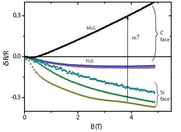
In this paper, low field magneto-resistance is used to correlate the transport properties, the growth conditions and the morphologies of epitaxially-grown graphene films elaborated from the different surfaces of 6H-SiC. The films studied have been grown with different graphene layer numbers, both from the Si and C terminated faces, some in ultra-high vacuum other in inert atmospheres. Depending on the SiC polytype and on the growth conditions, distinct surface morphologies can be observed which lead to very different magnetoresistance behaviors (see figure 1). Exploiting the unique features of interference phenomena present in magneto-transport, electronic properties can be related to the surface morphologies.
II Localization and anti-localization in graphene
Low field magneto-resistance is a sensitive probe for electronic transport as it measures the effect of quantum interferences along closed paths Bergmann (1982, 1984); Altshuler et al. (1980). Depending on the closed loop size, the interferences can be constructive or destructive. For very small loops, it has been demonstrated both theoretically McCann et al. (2006); Kechedzhi et al. (2007) and experimentally Wu et al. (2007); Tikhonenko et al. (2009) that interferences between identical time reversed paths are destructive in graphene leading to a negative magnetoconductance (positive magnetoresistance), which is characteristic of anti-localization of electron waves. For graphene, electron wavefunctions have four components and may be characterized by two additional quantum numbers: the isospin and the pseudospin. The isospin measures the relative wavefunction amplitude on the equivalent sites (A-B) in graphene unit cell, while the pseudospin measures to which band valley or the quantum states belong Castro Neto et al. (2009). Antilocalization is a characteristic feature of graphene as the isospin (collinear to momentum) undergoes a full rotation on a closed loop, changing the wavefunction sign and so forbidding the backscattering. As the loop size increases, scattering mechanisms lead to additional rotations of the isospin, as well as to the scattering between different valley states, such that the pseudospin need not be preserved on long paths. Two lengthscales characterize this diffusion: the pseudospin is controlled by the intervalley diffusion length , and the intravalley diffusion length controls the isospin random diffusion. The “overall” effect of these processes on the interferences along time-reversed paths is to change their sign back to the “normal” positive magneto-conductance due to coherent backscattering McCann et al. (2006); Kechedzhi et al. (2007) observed in other two-dimensional systems. Eventually, for extremely long paths (of length greater then , the phase coherence length) and/or high temperatures, inelastic scattering kills interferences. The beauty of quantum interference is that a characteristic magnetic field can be associated to every loop size, when half a flux quantum is threaded within the loop area: hence the magnetic fields can be associated to the lengthscales respectively.
| Face | growth | layer # | (m2/(Vs) | D(m2/s) | (4K) | ||
|---|---|---|---|---|---|---|---|
| C | UHV | 0.018 | 0.0025 | 72 nm | 40 nm | 26 nm | |
| C | Ar | 1.2 | 0.159 | 740 nm | |||
| Si | UHV | 2 | 0.012 | 0.0022 | 140 nm | 30 nm | 18 nm |
It is useful to recall some of the general features of epitaxial graphene on SiC. Graphene layers can be grown by Si sublimation at high temperature Hass et al. (2008a). Electrical conduction is known to be dominated by the completed layers closest to the interface Berger et al. (2006). When growing from the SiC C-face, there is a rotation between successive layers which effectively decouples the layers Hass et al. (2008b); Faugeras et al. (2008). This is to be contrasted from graphene layers grown from the Si face, where Bernal stacking breaks the symmetry between the two (A-B) carbon sites Hass et al. (2008a). In both cases, completed layers are continuous and ripples cover the SiC vicinal steps. Depending on the growth condition, folds are also observed. On ripples or folds, there is a local stretching of the graphene bonds. The other types of known defects arise at the graphene/SiC interface. Defects far from the graphene layer (at distance , where is graphene lattice constant) do not break the A-B symmetry and contribute only to intravalley elastic scattering. Sharp potential variations (), may break the graphene A-B symmetry locally. This scattering potential is time-reversal even and affects simultaneously the isospin and pseudospin and contribute both to the inter and intravalley scattering McCann et al. (2006); Kechedzhi et al. (2007). Ripples and folds stretch bonds and contribute equally to inter and intra valley scattering. Finally, trigonal warping contributes only to intravalley scattering McCann et al. (2006); Kechedzhi et al. (2007).
These scattering processes govern the crossover from localization at low field to anti-localization at high field. The quantum correction McCann et al. (2006); Kechedzhi et al. (2007) to the magneto-conductance of a single graphene layer can be split between the intervalley
| (1) |
and the intravalley contributions
| (2) |
where the function , and is the digamma function.
When the A-B symmetry is fully broken (for a bilayer on Si face, the two sublattices A and B are no more equivalent) the intravalley contributions have the opposite sign : the magnetoconductance increases monotonously with field and antilocalization disappears McCann et al. (2006); Kechedzhi et al. (2007).
III Results and discussion
Figure 1 gives an overview of all the magnetoresistance behaviors observed at 4K over a broader range of magnetic field. The transport properties have been measured using contacts pads evaporated through a mask with a Van der Paw geometry (surface of ). Four points DC measurements were performed down to . Films grown from the SiC C-face have larger mobilities and positive magnetoresistance at high fields. Thick films grown from the C-face (top trace) show a linear magnetoresistance at larger fields. The positive magnetoresistance observed at high field for SiC C-face samples can be contrasted with the SiC Si-face graphene which have lower mobilities and a negative magnetoresistance at all fields.
These differences can be understood in terms of weak localization and anti-localization in graphene. Using the appropriate weak-localization formulae, the intervalley, intravalley and phase coherence length can be obtained by fitting the magnetoconductance curves. All the results are summarized in table 1 and are discussed in the rest of this article.
III.1 Magneto-conductance on the Si-face of 6H-SiC
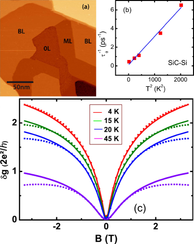
We first consider samples grown by graphitization of the SiC Si-face. The growth dynamics is slow and the average number of graphene layers can be controlled. When the number of layers exceeds one, the layers stack as in graphite (Bernal) and break the A-B symmetry. In the STM topographical image shown in Figure 2-a, the domains with different number of layers can be precisely identified and labelled. On average, this sample has layers and a mobility of 120 cm2/(V.s). STM studies have shown that the bilayers cover around of the surface of our sample. The upper graphene layer is continuous over the monolayer-bilayer junction Ji et al. (2011). The electron transmission between monolayer and bilayer graphene has been theoretically studied for zigzag and armchair boundaries. Due to the presence of an evanescent wave in the bilayer graphene, traveling modes are well connected to each other. The transmission through the boundary is strongly dependent on the incident angle Nakanishi et al. (2010). Nevertheless, the experimental measurements at the atomic scale have shown a poor transmission factor of and such junctions of monolayer-bilayer will reduce the macroscopic conductivity Ji et al. (2011). In our sample ,strong intervalley scattering was not observed at the single/bilayer edges in STM studies due to the smooth scattering potential in the continuous surface layer Mahmood et al. (2012). The magnetoconductance traces plotted in units of for different temperatures are shown in Figure 2-c: the continuous increase observed as a function of field saturates on the scale of . All curves can be fitted with the weak-localization formulae McCann et al. (2006); Kechedzhi et al. (2007) appropriate for bilayers, assuming that the phase coherence length is the only temperature dependent parameter. Despite the fact that the sample is inhomogeneous, we assume that the signal from the majority bilayer areas dominates the weak localization correction 111The weak localization of an inhomogeneous sample of mono- and bi-layer can be written as with and . Due to the fact that the diffusion constant is smaller for the monlayer the amplitude of is smaller than the amplitude of . which gives the magnetic field of the maximum of is larger than and the effect of is roughly to enlarge the magnetoresistance. Nevertheless the numerical results of the fits using the bilayer formulae seems correct.. The characteristic field T obtained from the fits is close to twice T. This ratio has been observed in most samples studied. Using , the intervalley and intravalley diffusion lengths are found to be comparable to the size of the flat terraces. This suggests that intervalley and intravalley scattering are dominated by the boundaries between domains. The time-reversed loops thus concern homogeneous domains. The corresponding timescales are set by the diffusion coefficient D for this 2D-sample. Using the fits, the dependence of the phase breaking rate on temperature, is shown in Figure 2-b. The behavior observed should be contrasted with the linear dependence observed for the C-face Wu et al. (2007). A quadratic increase of has also been observed at high temperatures by Tikhonenko et al. Tikhonenko et al. (2009). The linear contribution due to electron-electron dephasing appears to be quenched by the gap induced by Bernal stacking, leaving another scattering mechanism, probably associated with phonons, as the dominant one. For semiconductor 2D electronic systems, the electron-phonon scattering rate is known both from theory and experiments to increase as . For isolated graphene planes, different regimes Hwang and Das Sarma (2008) have been identified depending on the relative value of the temperature compared to the Bloch-Grüneisen temperature ( for this sample): below , the rate grows as , while it is linear above Stauber et al. (2007). How the SiC substrate affects this behavior is not known. While the fits (Figure 2-c) are quite accurate at low fields, deviations can be observed at high temperature and high fields: a negative component in the magnetoresistance traces grows at large fields as the temperature is raised. The origin of this classical-like behavior is not clear, but it is concomitant with the appearance of the quadratic dephasing rate.
III.2 Magneto-conductance on the C-face of 6H-SiC

Samples grown from SiC C-face have notably different morphologies when grown in high vacuum or in an inert atmosphere. When grown in ultra-high vacuum, flat terraces are relatively small as shown on the topographic STM image (Figure 3-a top-left), typically of order 60 nm with folds and ripples at their boundaries. When grown in an inert atmosphere, the domains (and mobilities) are much larger (see figure 4).
As long as the number of layers is small (), it is possible to analyze the magneto-conductance in term of the weak localization-antilocalization effects discussed above, in agrement with earlier studies Wu et al. (2007); Tikhonenko et al. (2009); Creeth et al. (2011). This is illustrated in the bottom panel of Figure 3-c, where the magnetoconductance traces of a UHV grown sample, scaled in units of , are plotted for different temperatures. All traces can be fitted to the weak localization correction discussed in equations 1 and 2. In particular, the weak localization dip observed at low field (i.e. for the longest coherent retrodiffusion loops) turns into a negative magnetoconductance at higher fields (anti-localization for small retrodiffusion loops). The characteristic field T is found to be nearly twice T as for the Si-face grown samples. The corresponding intervalley and intravalley diffusion length are also of the order of the size of the flat terraces (see the table 1). All traces can be fitted assuming that only varies with temperature. The dependence of the dephasing rate with is shown in Figure 3-b. The linear temperature dependence, also observed in Wu et al. Wu et al. (2007) is consistent with Altshuler-Aronov prediction for electron-electron interactions Altshuler and Aronov (1985); Aleiner et al. (1999) with is the quantum resitance and is the square resistance. The measured slope (s-1K-1) is an order of magnitude larger than the expected value. Similar discrepancies are not uncommon in other semiconducting 2DEG systems. Among the other sources of dephasing, the Coulomb scattering of electrons in different layers have been shown theoretically to be relevant Darancet et al. (2008). Electron-phonon scattering may also contribute Stauber et al. (2007); Hwang and Das Sarma (2008).
III.3 Thick graphene sample
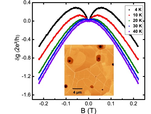
We now turn to samples graphitized from the SiC C-face in an inert atmosphere which have significantly different morphologies and transport behaviors. When graphitizing from the SiC C-face, the number of layers increases rapidly and a larger number of graphene layers (of order of 30-50 for the sample studied) is reached in a 10 minutes period. After annealing at high temperature, the sample morphology (as shown in the AFM image 4-inset) shows very large (several m) domains separated by fold or ripples. The magnetoconductance traces measured at different temperatures are shown in Figure 4. A narrow weak localization dip close to zero field is clearly seen: its width is controlled by the phase coherence length (of the order of 750 nm at 4 K). The diffusion coefficient (1600 cm2/s) and mobilities (cm2/(V.s)) are also found to be much larger than in the UHV grown samples.
Within this thick sample, the conduction is no longer limited to the layer closest to the interface with the SiC. From the measured value of the diffusion coefficient, we infer a large mean free path which comparable to . For the semi-classical theory, the curvature of electron trajectories usually results in a positive quadratic magneto-resistance and so a negative magneto-conductance : with the conductivity without magnetic field and the relativistic graphene cyclotron frequency. A fit to the magnetoconductance shown in Fig. 4 gives a scattering time ps shorter than the mean-free time ps suggesting other scattering processes are at play in a magnetic field (Coulomb scattering between layers Darancet et al. (2008), tunneling between graphene plane) which contribute to the broadening of Landau levels and shorten the effective scattering times. The amplitude of the negative magnetoconductance above 0.05 T shown in Fig. 4 also exceeds and cannot be attributed to quantum interference alone. Assuming relativistic electron dynamics, the cyclotron radius becomes smaller than the mean free path for fields exceeding ( T). As seen in Fig. 4, the magnetoconductance turns negative above T (). At larger field(), a linear magnetoresistance regime is observed (the top curve in Fig. 1), which is consistent with previous transport measurements on epitaxial graphene Friedman et al. (2010). Several routes to linear magnetoconductance have been previously considered. For inhomogeneous and disordered materials, a classical resistor network model Parish and Littlewood (2003, 2005) accounts for the linear magnetoresistance observed in silver chalcogenides. Another mechanism leading to a linear magnetoconductance has been considered by AbrikosovAbrikosov (1999, 2000) for layered materials and small (and zero) gap 3d-semiconductors: in the quantum limit, when the temperature and Fermi energy are smaller than the Landau band splitting, the magnetoresistance becomes linear. For a pure 2d system, the requirements for quantum linear magnetoresistance coincide with the quantum Hall regime. On these samples, the onset of the linear regime (0.5 T) which coincides approximatively to occurs well before the Shubnikov-de Haas oscillations are observed 222For the sample obtained in UHV, the poor mobility imply that the quantum hall regime is obtained at higher magnetic fields. Thus the linear magnetoresistance regim cannot be reached for the range of magnetic field values used in this study. This indicates that tunneling between layers is larger in these thick graphene samples compared to the few layer samples (number of layers . This makes the Abrikosov mechanism the most probable explanation for the linear magnetoresitance, in agreement with Ref.Friedman et al. (2010). From a device point of view, the transport characteristics of such thick graphene stack are good. Gating effects measured on such thick graphene stacks have however been found to be small.
III.4 Discussion of the intravalley versus intervalley scattering length
The quasiparticles of graphene can be described in the space of four-component wave functions, basis describing electronic amplitude on and sites and in the valleys and . In order to describe the microscopic scattering potentials, we introduce two sets of hermitian matrices : the isospin () and the pseudospin () McCann et al. (2006); Kechedzhi et al. (2007). Then the electron hamiltonian in weakly disorder graphene can be parameterized as
| (3) |
For each scattering potential , there is a microscopic scattering rate . Since and are equivalent (), there are only four microscopic scattering rates, and . If the sample is sufficiently disordered, it is plausible to assume that all the potential and scattering rates are comparable. In this limit, the inter and intravalley scattering rates Kechedzhi et al. (2007) and since . is found to be twice in agreement with our experimental results, and the weak localization correction depends only on as : there is a universal scaling of the magnetoconductance in and all samples-magnetoconductances collapse on this curve at low temperatures.
IV Conclusions
In this paper, an overview of weak localization properties on a variety of epitaxially grown samples has been presented. For all types of few-layers graphene samples, the measured characteristic lengthscales for iso and pseudo-spin diffusion (intra/intervalley scattering) coincide with the terrace and or domain sizes identified on the samples by STM or AFM images. For most samples, the magnitude of the intervalley and intravalley scattering rates have a ratio of . Such a ratio is found when all scattering rates induced by the scattering potentials (cf. Eq. 3) () are of similar magnitude. The propagation through a domain is ballistic and most of the diffusion occurs at the edge of the terraces where all types of scattering processes are present. In the case of thick samples grown in furnace, the elastic mean free path is smaller than the domains’ size and the propagation through a domain is no more ballistic but diffusive. Other scattering processes are involved like coulomb scattering between layers or tunneling between graphene plane.
Acknowledgements.
We acknowledge L. Magaud for her critical reading of this article. This work is supported by the French National Research Agency (GraphSiC and XPgraphene projects) and the Nanosciences Foundation (DISPOGRAPH project).References
- Novoselov et al. (2005) K. S. Novoselov, A. K. Geim, S. V. Morozov, D. Jiang, M. I. Katsnelson, I. V. Grigorieva, S. V. Dubonos, and A. A. Firsov, Nature 438, 197 (2005).
- Zhang et al. (2005) Y. B. Zhang, Y. W. Tan, H. L. Stormer, and P. Kim, Nature 438, 201 (2005).
- Berger et al. (2004) C. Berger, Z. M. Song, T. B. Li, X. B. Li, A. Y. Ogbazghi, R. Feng, Z. T. Dai, A. N. Marchenkov, E. H. Conrad, P. N. First, and W. A. de Heer, Journal of Physical Chemistry B 108, 19912 (2004).
- Moreau et al. (2010) E. Moreau, F. J. Ferrer, D. Vignaud, S. Godey, and X. Wallart, Physica Status Solidi a-Applications and Materials Science 207, 300 (2010).
- Coraux et al. (2008) J. Coraux, A. T. N’Diaye, C. Busse, and T. Michely, Nano Letters 8, 565 (2008).
- Kim et al. (2009) K. S. Kim, Y. Zhao, H. Jang, S. Y. Lee, J. M. Kim, K. S. Kim, J. H. Ahn, P. Kim, J. Y. Choi, and B. H. Hong, Nature 457, 706 (2009).
- Li et al. (2009) X. S. Li, W. W. Cai, J. H. An, S. Kim, J. Nah, D. X. Yang, R. Piner, A. Velamakanni, I. Jung, E. Tutuc, S. K. Banerjee, L. Colombo, and R. S. Ruoff, Science 324, 1312 (2009).
- Robinson et al. (2009) J. A. Robinson, M. Wetherington, J. L. Tedesco, P. M. Campbell, X. Weng, J. Stitt, M. A. Fanton, E. Frantz, D. Snyder, B. L. VanMil, G. G. Jernigan, R. L. Myers-Ward, C. R. Eddy, and D. K. Gaskill, Nano Letters 9, 2873 (2009).
- Low et al. (2012) T. Low, V. Perebeinos, J. Tersoff, and P. Avouris, Phys. Rev. Lett. 108, 096601 (2012).
- Tanabe et al. (2010) S. Tanabe, Y. Sekine, H. Kageshima, M. Nagase, and H. Hibino, Applied Physics Express 3, 075102 (2010).
- Ji et al. (2011) S.-H. Ji, J. B. Hannon, V. Tromp, R. M .and Perebeinos, J. Tersoff, and F. M. Ross, Nature Materials 11, 114 (2011).
- Lin et al. (2010) Y.-M. Lin, C. Dimitrakopoulos, D. B. Farmer, S.-J. Han, Y. Wu, W. Zhu, D. D. Kurt Gaskill, J. L. Tedesco, R. L. Myers-Ward, C. R. Eddy, A. Gril, and P. Avouris, Applied Physics Letters 97, 112107 (2010).
- Lee et al. (2011) K. Lee, S. Kim, M. S. Points, T. E. Beechem, T. Oht, and E. Tutuc, NanoLetters 11, 3624 (2011).
- Jobst et al. (2010) J. Jobst, D. Waldmann, F. Speck, R. Hirner, D. K. Maude, T. Seyller, and H. B. Weber, Phys. Rev. B 81, 195434 (2010).
- Creeth et al. (2011) G. L. Creeth, A. J. Strudwick, J. T. Sadowski, and C. H. Marrows, Phys. Rev. B 83, 195440 (2011).
- Lara-Avila et al. (2011) S. Lara-Avila, A. Tzalenchuk, S. Kubatkin, R. Yakimova, T. J. B. M. Janssen, K. Cedergren, T. Bergsten, and V. Fal’ko, Phys. Rev. Lett. 107, 166602 (2011).
- Bergmann (1982) G. Bergmann, Solid State Communications 42, 815 (1982).
- Bergmann (1984) G. Bergmann, Physics Reports-Review Section of Physics Letters 107, 1 (1984).
- Altshuler et al. (1980) B. L. Altshuler, D. Khmel’nitzkii, A. I. Larkin, and P. A. Lee, Physical Review B 22, 5142 (1980).
- McCann et al. (2006) E. McCann, K. Kechedzhi, V. I. Fal’ko, H. Suzuura, T. Ando, and B. L. Altshuler, Physical Review Letters 97, 146805 (2006).
- Kechedzhi et al. (2007) K. Kechedzhi, E. McCann, V. I. Fal’ko, H. Suzuura, T. Ando, and B. L. Altshuler, European Physical Journal-Special Topics 148, 39 (2007).
- Wu et al. (2007) X. S. Wu, X. B. Li, Z. M. Song, C. Berger, and W. A. de Heer, Physical Review Letters 98, 136801 (2007).
- Tikhonenko et al. (2009) F. V. Tikhonenko, A. A. Kozikov, A. K. Savchenko, and R. V. Gorbachev, Physical Review Letters 103, 226801 (2009).
- Castro Neto et al. (2009) A. H. Castro Neto, F. Guinea, N. M. R. Peres, K. S. Novoselov, and A. K. Geim, Reviews of Modern Physics 81, 109 (2009).
- Hass et al. (2008a) J. Hass, W. A. de Heer, and E. H. Conrad, Journal of Physics-Condensed Matter 20, 323202 (2008a).
- Berger et al. (2006) C. Berger, Z. M. Song, X. B. Li, X. S. Wu, N. Brown, C. Naud, D. Mayou, T. B. Li, J. Hass, A. N. Marchenkov, E. H. Conrad, P. N. First, and W. A. de Heer, Science 312, 1191 (2006).
- Hass et al. (2008b) J. Hass, F. Varchon, J. E. Millan-Otoya, M. Sprinkle, N. Sharma, W. A. De Heer, C. Berger, P. N. First, L. Magaud, and E. H. Conrad, Physical Review Letters 100, 125504 (2008b).
- Faugeras et al. (2008) C. Faugeras, A. Nerriere, M. Potemski, A. Mahmood, E. Dujardin, C. Berger, and W. A. de Heer, Applied Physics Letters 92, 0119214 (2008).
- Lauffer et al. (2008) P. Lauffer, K. V. Emtsev, R. Graupner, T. Seyller, L. Ley, S. A. Reshanov, and H. B. Weber, Physical Review B 77, 155426 (2008).
- Nakanishi et al. (2010) T. Nakanishi, M. Koshino, and T. Ando, Phys. Rev. B 82, 125428 (2010).
- Mahmood et al. (2012) A. Mahmood, P. Mallet, and J.-Y. Veuillen, Nanotechnology 23, 055706 (2012).
- Hwang and Das Sarma (2008) E. H. Hwang and S. Das Sarma, Physical Review B 77, 115449 (2008).
- Stauber et al. (2007) T. Stauber, N. M. R. Peres, and F. Guinea, Physical Review B 76, 205423 (2007).
- Altshuler and Aronov (1985) B. L. Altshuler and A. Aronov, in Electron-Electron Interactions in Disordered Systems, Modern problems in condensed matter science, Vol. 10, edited by A. L. P. M. Efros (North-Holland, Amsterdam, 1985) pp. 1–150.
- Aleiner et al. (1999) I. L. Aleiner, B. L. Altshuler, and M. E. Gershenson, Waves in Random Media 9, 201 (1999).
- Darancet et al. (2008) P. Darancet, N. Wipf, C. Berger, W. A. de Heer, and D. Mayou, Physical Review Letters 101, 116806 (2008).
- Friedman et al. (2010) A. L. Friedman, J. L. Tedesco, P. M. Campbell, J. C. Culbertson, E. Aifer, F. K. Perkins, R. L. Myers-Ward, J. K. Hite, C. R. Eddy, G. G. Jernigan, and D. K. Gaskill, Nano Letters 10, 3962–3965 (2010).
- Parish and Littlewood (2003) M. M. Parish and P. B. Littlewood, Nature 426, 162 (2003).
- Parish and Littlewood (2005) M. M. Parish and P. B. Littlewood, Physical Review B 72, 094417 (2005).
- Abrikosov (1999) A. A. Abrikosov, Physical Review B 60, 4231 (1999).
- Abrikosov (2000) A. A. Abrikosov, Europhysics Letters 49, 789 (2000).