Note: Cryogenic microstripline-on-Kapton microwave interconnects
Abstract
Simple broadband microwave interconnects are needed for increasing the size of focal plane heterodyne radiometer arrays. We have measured loss and cross-talk for arrays of microstrip transmission lines in flex circuit technology at 297 and 77 K, finding good performance to at least 20 GHz. The dielectric constant of Kapton substrates changes very little from 297 to 77 K, and the electrical loss drops. The small cross-sectional area of metal in a printed circuit structure yields overall thermal conductivities similar to stainless steel coaxial cable. Operationally, the main performance tradeoffs are between crosstalk and thermal conductivity. We tested a patterned ground plane to reduce heat flux.
pacs:
07.57.-c, 84.40.Az, 44.10.+iI Introduction
Simple broadband microwave interconnects are key components for arrays of focal plane heterodyne radiometers. Here we report on an investigation of transmission line arrays printed on flexible circuit board substrates, part of a program to develop and assess components for a scalable millimeter-wave focal plane radiometerSieth et al. (2012). For tens of focal plane elements, microwave intermediate frequency signals can be routed on individual semi-rigid coaxial cables, but this approach becomes cumbersome for large focal plane arrays. Here we report on an alternative interconnect: microstripline on a polyimide (KaptonTrademark of DuPont Electronic Technologies, Research Triangle Park, NC ) flex circuit substrate. A number of papersOliver (2009, 2010); McGibney et al. (2011), among others, report microwave characterization of flex substrates, but none that we are aware of report cryogenic properties.
Of the well-developed planar transmission line structures, we choose microstripline because of its mechanical simplicity, its relatively low electrical loss, and because it requires the least metal of common planar transmission lines. The last item is an important consideration for transmission lines between components at different temperatures. In spite of copper’s high thermal conductivity, the small metallic cross-section of planar lines results in a total heat flow along a flex circuit comparable to that through the much larger cross-sections of stainless steel and steel in standard cryogenic coaxial cable. With strength carried by the Kapton substrate, and high-frequency fields confined to a thin layer near the conductor surfaces by the skin effect, very thin conductors are practical for the lines. The thinnest standard copper cladding on Kapton is 0.5 oz. per square foot, or 0.7 mil (0.0007 in, m) thick. Calculated microstrip/coax heat flow ratios for typical thermal conductivitiesScott (1959) along an 8-circuit evaluation structure (8 parallel 11 mil strips on an 850 mil wide ground plane) divided by that along 8 stainless-steel 085 coaxial cables are 0.66 for 297 K–77 K end temperatures, and 2.9 for 77 K–20 K. For microstriplines most of the thermal path is in the ground plane, so we investigated a patterned ground plane that reduced the amount of metal.
We report measurements on two test structures. The first included microwave resonators to evaluate materials properties at 297 and 77 K (room temperature and liquid nitrogen). The second was a set of 8 parallel microstrip lines to evaluate multiple-line performance over two ground plane patterns. Both structures were on DuPont Pyralux AP-8555R stock, which has 0.5 oz/ft2 rolledOliver (2009) copper bonded to both sides of 5 mil thick polyimide substrate material. Although thinner substrates are available, we chose 5 mil mostly because of fabrication tolerances: with this thickness, the microstrip lines are 11 mils wide, and a 10% width fabrication error still produces a line with an impedance close to . As secondary considerations, electrical loss drops with increasing strip width, and an 11 mil width is suitable for solder contact between SMA connector pins and the strip. Most flex circuits have a thin dielectric coverlay to protect the traces, but the adhesive has high electrical loss at microwave frequenciesOliver (2009), so the test structures had no coverlays.
II Tee resonator measurements at 297 and 77 K
A commercial firm fabricated transmission line test structures on a 1.5 inch by 4.1 in substrate with a full ground plane on one side and three microstrip transmission lines across the short dimension on the other side. Two of the lines had perpendicular shunt open stubs to make tee resonators, with stub lengths 3.000 and 0.550 inch long. Johnson 142-0701-851 edge connectors with 10 mil diameter pins made contact with the lines and ground pads to either side of the line. Gold plating (5 in of gold on 100 in nickel) kept the traces from oxidizing while allowing wire bond and solder connections.
The substrate shrinks little between room temperature and 77 K while remaining flexible. There was no apparent bending or other thermally induced stress between the substrate and fully metalized ground plane when the test structure was immersed in liquid nitrogen. We corrected for resonator length change with cooling by measuring the length of the test substrate at room temperature and when immersed with a stainless steel scale in a shallow tray filled with liquid nitrogen; the length change on cooling was only 5 mil on the scale. After correcting for the scale’s own fractional length contraction from 293–77 Khttp://cryogenics.nist.gov/MPropsMAY/materialproperties.htm we derived a substrate fractional length contraction of between 297 and 77 K. At 77 K, the 3 inch resonator was shorter by 13 mils.
All resonator measurements were in vacuum with the substrate attached to the cold plate of a small liquid nitrogen cryostat. A copper radiation shield attached to the cold plate and lined with microwave absorber covered the substrate to block infrared radiation that would otherwise heat the substrate. Comparison of warm transmission with and without the copper cover showed that the cover did not affect microwave transmission. Conformable 085 coaxial cables, 8 in long, connected the test structure to hermetic SMA feedthroughs passing through the cryostat wall; 3 dB attenuators between the cables and feedthroughs helped reduce residual standing waves. We made measurements of the resonators and the through on the test structure at 297 and 77 K with an Agilent 8722D vector network analyzer, sampling 201 points from 50 MHz to 20 GHz.
Dividing the test structure’s resonator transmission () by that of the through line removed cable, attenuator, and connector losses, giving a clean measurement of the tee resonator alone. We used Microwave OfficeMicrowave Office, AWR Corp., El Segundo, CA (MWO) for this division and to fit for substrate dielectric constant and loss tangent by comparing the derived values of to those from MWO’s parametric models (which include finite-element electromagnetic calculations for the discontinuities at the tee) and optimization function. The topmost lines in Figure 1 display the cold measurement and the MWO model fit for the 3 in resonator. Plots of the residuals between the two, as well as the residual for the warm measurements, shows that the models are good representations at both temperatures. Structure at higher frequencies is common to both warm and cold resonators and is probably due to different connector mismatches in the resonator and through lines. The overall agreement between measurement and theory indicates that the materials parameters we derive are valid to at least 20 GHz.
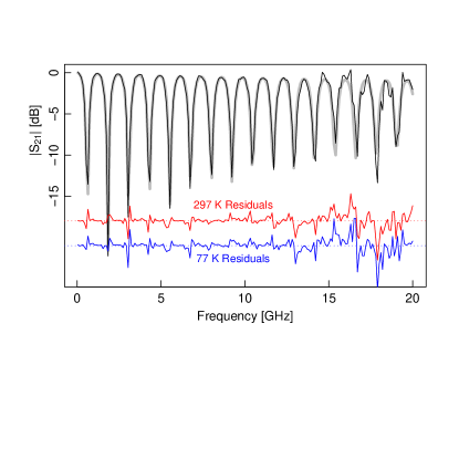
Table 1 summarizes derived electrical properties. The dielectric constant changed by a negligible amount between room temperature and 77 K; a representative value for microwave frequencies is . There is a weak dependence on the fit frequency range, 0.05 GHz to , for , which is just visible in plots for different frequencies. Both dielectric and metalization losses contribute to overall loss, but the fits were insensitive to losses in the metal, parametrized by conductivity relative to gold, and we used a value of . Loss in the dielectric drops by a factor of approximately two on cooling, from to 0.007.
| GHz | ||||
|---|---|---|---|---|
| 3 | 3.378 | 3.377 | 0.008 | 0.000 |
| 6 | 3.372 | 3.370 | 0.012 | 0.006 |
| 12 | 3.348 | 3.350 | 0.013 | 0.007 |
III Loss and cross-talk with parallel lines at 297 K
We directly assessed the performance of microwave interconnects with a structure with eight parallel microstrip transmission lines with strip widths of 11 mil on 100 mil centers (gaps between lines equal to 8.1 times the strip widths). The minimum line length was 8.5 in, and the maximum was 11.7 in. As shown in Figure 2, four of the lines were over a solid ground plane, and the other four were over a patterned ground plane with reduced thermal conductivity. The patterning was a solid plane 55 mils wide below each 11 mil-wide line, providing termination for most of the field lines, with 10 mil-wide cross-strips on 80 mil centers tying the grounds together across the width of the structure. The cross-strips must have spacing with distance well below a quarter of the shortest wavelength to avoid resonances between the lines, and or closer to reduce structure in . With a pattern of relatively narrow ground planes under the lines, joined by thin cross-connects, the calculated heat flow along the structure is a factor of three lower than a solid ground plane. Broader ground strips under the lines would reduce cross talk at the cost of higher thermal conductivity. Reducing line widths on a thinner substrate is an additional attractive solution at low temperatures, where the electrical loss is lower, although fabrication tolerances may become critical.
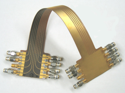
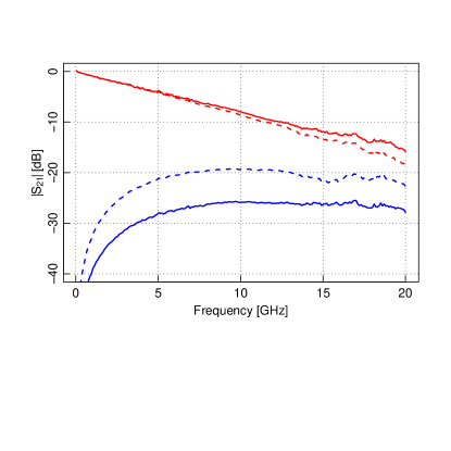
Figure 3 shows the transmission loss and cross-coupling for the 10.6 inch lines over the two ground planes. Cross-coupling in this plot is to a nearest-neighbor line with 8.2 inches of parallel run; the nearest neighbor on the other side has 8.8 inches of parallel run. The transmission loss is only slightly higher for the patterned ground plane, but the cross talk is substantially higher: the far-out field lines carry little power but are responsible for cross-coupling, and are poorly terminated on the strips between the transmission lines.
Transmission loss for this structure with a solid ground plane is closely 0.076 dB/GHz/in. A model fit over 0.05 GHz–12 GHz gives , slightly higher than the fit to the room-temperature resonator data, . Loss from cross-coupling between lines is present and is accurately predicted by coupled-line microstrip theory. Modeling for other spacings shows cross-talk decreases with increasing spacing and frequency, but has periodic maxima with line length, as expected for a forward-coupled pair of linesIkalainen and Matthaei (1987): MWO calculations yield 20 dB maxima for gaps of 6.5 time the strip widths, and 30 dB for 12 times the strip widths. For comparison, standard 085 semi-rigid cryogenic coaxial cable (stainless steel outer jacket, Teflon insulation, silver-plated steel wire center conductor) has a loss of about 0.0125 dB/GHz/in and essentially infinite isolation, but with little possibility for mass connection.
Acknowledgements.
This work was supported by NSF grant ATI-0905855 (ARRA). We thank AWR for providing access to Microwave Office under its University Program. We benefited from conversations with Dr. M. Morgan of the National Radio Astronomy Observatory.References
- Sieth et al. (2012) M. Sieth, S. Church, J. M. Lau, P. Voll, T. Gaier, P. Kangaslahti, L. Samoska, M. Soria, K. Cleary, R. Gawande, A. C. S. Readhead, R. Reeves, A. Harris, J. Neilson, S. Tantawi, and D. Van Winkle, ArXiv e-prints 1204.3125 (2012).
- (2) Trademark of DuPont Electronic Technologies, Research Triangle Park, NC, .
- Oliver (2009) G. Oliver, “High speed material considerations for flex and rigid-flex circuit designs,” Tech. Rep. (DuPont Electronic Technologies, 2009) presentation at IPC Flex Show, Minneapolis, MN.
- Oliver (2010) G. Oliver, “Electrical characterization of flexible circuit materials at high frequency,” Tech. Rep. (DuPont Electronic Technologies, 2010) presentation at DesignCon 2010.
- McGibney et al. (2011) E. McGibney, J. Barton, L. Floyd, P. Tassie, and J. Barrett, Components, Packaging and Manufacturing Technology, IEEE Transactions on 1, 4 (2011).
- Scott (1959) R. B. Scott, Cryogenic Engineering (van Nostrand Co., Inc., New York, 1959).
- (7) http://cryogenics.nist.gov/MPropsMAY/materialproperties.htm, .
- (8) Microwave Office, AWR Corp., El Segundo, CA, .
- Ikalainen and Matthaei (1987) P. Ikalainen and G. Matthaei, Microwave Theory and Techniques, IEEE Transactions on 35, 719 (1987).