Effect of transport-induced charge inhomogeneity on point-contact Andreev reflection spectra at ferromagnet-superconductor interfaces
Abstract
We investigate the transport properties of a ferromagnet-superconductor interface within the framework of a modified three-dimensional Blonder-Tinkham-Klapwijk formalism. In particular, we propose that charge inhomogeneity forms via two unique transport mechanisms, namely, evanescent Andreev reflection and evanescent quasiparticle transmission. Furthermore, we take into account the influence of charge inhomogeneity on the interfacial barrier potential and calculate the conductance as a function of bias voltage. Point-contact Andreev reflection (PCAR) spectra often show dip structures, large zero-bias conductance enhancement, and additional zero-bias conductance peak. Our results indicate that transport-induced charge inhomogeneity could be a source of all these anomalous characteristics of the PCAR spectra.
I Introduction
Measurement of spin polarization is an important subject in spintronics. The point-contact Andreev reflection (PCAR) technique has been widely used as a simple and powerful method in the determination of conduction electron spin polarization in a broad range of ferromagnetsUpadhyay ; Soulen ; Ji01 . The principle behind the spin polarization measurement by the PCAR spectroscopy is based on the fact that the Andreev reflectionAndreev probability at a ferromagnet-superconductor interface is limited by the minority spin carrier density at the Fermi level in the ferromagnet. In the limit of a clean ballistic ferromagnet-superconductor contact, the spin polarization is simply determined by the ratio of the conductances and at zero and high bias voltage, respectively, which was obtained by decomposing the current into a fully polarized part and a fully unpolarized part.Upadhyay ; Soulen However, for real ferromagnet-superconductor contacts, which are generally not in the clean limit, accurate determination of is nontrivial and usually requires a careful analysis of the complete conductance-voltage () curve.Ji01 Blonder et al. Blonder developed a theory (known as the BTK model) that takes into account the Andreev reflection, for the experimental curves of normal metal-superconductor contacts with different behaviors ranging from metallic to tunnel junction. Later, Strijkers et al. Strijkers extended the BTK model to a ferromagnet-superconductor contact by including the effects of the spin polarization in the ferromagnet. The extended BTK model of Strijkers et al. has been applied to analyze the curves of many ferromagnet-superconductor contacts and also to determine the spin polarization in the ferromagnets in the contacts.Ji01 ; Strijkers In addition to the original one-dimensional (1-D) BTK modelBlonder and the extended 1-D BTK modelStrijkers , several extended three-dimensional (3-D) BTK models for both ballistic and diffusive regimes have also been proposed.Golubov ; Chalsani ; Mortensen ; Mazin
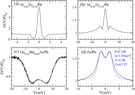
Interestingly, anomalous phenomena such as the dip structures Soulen ; Nowack ; Srikanth ; DeWilde1 ; DeWilde2 ; Walti ; Laube ; Mao ; Gourgy ; Daghero , the zero-bias conductance peak (ZBCP) Srikanth ; Kastalsky ; Magnee ; Quirion , and the large zero-bias enhancement Mao , may appear in the PCAR spectra of a wide variety of point contact systems. For example, Fig. 1(a) shows that unexpected dips emerge when the bias voltage approaches the superconducting energy gap . In addition, a narrow peak occurs at (known as the ZBCP), as shown in Fig. 1(b) and (c). The large zero-bias enhancement may result in the normalized zero-bias conductance being larger than 2.0 [see Fig. 1(a)]. These characteristics cannot be explained by the above-mentioned extended BTK models Blonder ; Strijkers ; Soulen ; Golubov ; Chalsani ; Mortensen ; Mazin and thus other effects must be taken into account.
The physical origins of the dips, ZBCP, and large zero-bias enhancement have been studied before. For example, Strijkers et al.Strijkers investigated the dip structures by introducing an additional proximity-induced superconducting energy gap. On the other hand, intergrain Josephson effectShan and Maxwell resistanceSheet were also regarded as possible sources of both dips and large zero-bias enhancement. Schmidt et al.Schmidt proposed formation of superconductor-insulator-superconductor (SIS) junctions that would result in the ZBCP. Indeed, the geometry of a point contact may lead to the formation of a SIS junction. However, the ZBCP also appears in planar superconductor-insulator-normal metal (SIN) junctionsMao . In ref. Geresdi , the ZBCP was explained by multiple phase-coherent reflections and proximity-induced Josephson effect. However, this explanation is inapplicable for the material with large exchange splitting. Furthermore, the authors did not provide any model to fit their experimental data. Interestingly, the Andreev bound statesTanakaKashiwaya have also been considered as a source of the ZPCP. A recent theoretical work further showed that an Andreev bound state could be viewed as a topological edge stateTanaka . However, an Andreev bound state stems from the unconventional pairing symmetry and thus would not occur in s-wave superconductors. Therefore, the origins of the dip structures, zero-bias enhancement, and ZBCP are still not fully understood.
In addition to the above-mentioned anomalous features, for some experimental data, the value of the fitted model parameters for the extended BTK model of Strijkers et al.Strijkers , e.g., , is much larger than the well-known value. For example, in Fig. 1(d), the energy gap of Pb is 1.35 meV, whereas the fitted value is 1.93 meV. Such PCAR spectra which exhibit a broadened energy gap, are called broadened spectra. However, two plausible mechanisms: thermal effectsKant ; Auth ; Bugoslavsky ; Baltz and a spreading resistanceWoods ; Chiang ; Chen2 , have been proposed to explain the broadened spectra.
In this paper, we investigate the transport mechanism of a ferromagnet-superconductor interface and develop a modified BTK model to better describe the physics at the interface and account for anomalous PCAR spectra. We solve a 3-D Bogolubov de-Gennes equations, assuming no scattering along the transverse direction. We find that evanescent waves form for the large-angle incidence. We point out that these evanescent waves might lead to charge inhomogeneity and an electric dipole layer occurs at the interface. Furthermore, we take the effect of charge inhomogeneity into account by modifying the barrier strength . Interestingly, by doing that, we establish a new 3-D BTK model which can describe the anomalous conductance spectra with dip structures, a zero-bias conductance peak, and large zero-bias enhancement. In other words, we show that all anomalous conductance spectra have the same origin: transport induced charge inhomogeneity. We also discuss the temperature-dependence of the dip structures. Futhermore, we fit the experimental results using this new model including the effect of spreading resistance. We find that not only the ZBCP spectra but also unsual spectra could be fitted well by our model.
II Theoretical model
We begin with the 3-D Bogolubov de-Gennes Hamiltonian.
| (5) | |||
| (8) | |||
| (9) |
Here, exchange potential and pair potential , the -axis is normal to the interface. The ferromagnet and superconductor are on the left and right side of the interface, respectively (see Fig. 2). denotes up (down) spin and () is 1 (-1). Like other BTK formalisms, we model the interface scattering by a delta-function potential . In addition, we define the spin polarization
| (10) |
where () and () are density of states and Fermi velocity for spin-up (down) electrons, respectively. We obtain . Furthermore, we assume the and terms are negligible and hence obtain the wave vectors for electrons, holes, and quasiparticles in superconductor , , , respectively. Here, .
II.1 Incident angle and Andreev reflection
We consider all possible incident angles which vary from to Mortensen ; Chalsani and assume no scattering parallel to the interface (i.e. the transverse component of wave vector is the same in the ferromagnet and superconductor) Mortensen . We then derive the eigenstates of the Bogolubov de-Gennes Hamiltonian.
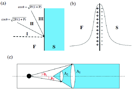
By matching the transverse components of wave vectors at the boundary, we find that with for the spin-up incident electrons, the forms of wave functions could be separated into three distinct regions, as shown in Fig. 2(a). When the angle of incidence is less than , wave functions do not decay. Conversely, when the incident angle is larger than , the Andreev reflected hole becomes evanescent. Increasing the incident angle above , the transmitted states in the superconductor (i.e. electron-like and hole-like states) start to decay and cannot propagate. Therefore, we use the two boundary conditions: and to match the wave functions for the three regions, separately. Here, is the barrier strength. Following the original BTK modelBlonder , is defined by .
In region I (i.e. ), the wave functions in the ferromagnet and superconductor read as follows.
| (11) |
In region II (i.e. ), unlike region I, we take into account the evanescent hole state and hence is written as
| (12) |
However, is the same as in region I.
In region III (i.e. ), in addition to the evanescent Andreev reflected hole, the transmitted waves decay exponentially and hence we have to rewrite as,
| (13) |
where and have the same definition as in ref. Blonder . The wave vectors in the -direction are , , and . The decay parameters , and . denotes the Fermi wave vector.
As to the spin-down incident electron, the wave functions never decay regardless of how large the incident angle is. Therefore, the forms of wave functions are the same as that in region I except the wave vectors are different. The wave vectors in the -direction for the spin-down incident electron are , , and .
The wave vectors of the incident electron and the Andreev reflected hole are not equal. This indicates that the reflected hole does not retrace the path of the incident electron, as in the usual Andreev reflection process. As pointed out in ref. Kashiwaya , for the 3-D model, in the presence of the exchange interaction, the retro-reflectivity of Andreev reflection would be broken. Recently, it was shown that specular Andreev reflection may happen in graphene metal-superconductor structuresBeenakker1 ; Hsu . As to the decaying waves at larger incident angle, they stand for the states localized near the interfaceKatsnelson . After matching wave functions at the interface, we can obtain the amplitudes of the Andreev reflection , normal reflection , electron-like transmission , and hole-like transmission and hence the probabilities for each region.
In addition, it should be noted that evanescent Andreev reflection and evanescent quasiparticles transimission would also happen for a normal metal-superconductor interface. The evanescent Andreev reflection and quasiparticle transmission occur when and . When (), [] for any incident angle. Therefore, the inequality of wave vector is a necessary condition for the formation of the evanescent states. For higher spin polarization (ferromagnet), the inequality of wavectors is mainly caused by the exchange splitting. Hence, it is reasonable to neglect the terms of and for mathematical simplication. However, when the spin polarization is close to zero, and are not negligible compared to the exchange splitting. For , if we keep and in wave vectors, the wavectors of the incident electron and Andreev reflected hole are given by , , , and . Here, and are the wave vectors of electron-like and hole-like states, respectively. In the presence of and , therefore, the evanescent Andreev reflection and quasiparticle transmission would appear in the normal metal-superconductor point contacts as well. Our mathematical formulae presented in this paper are applicable for the ferromagnet-superconductor interfaces only. In the future, we will study the evanescent transport at normal metal-superconductor interfaces.
II.2 Modification of barrier strength
| 0 | ||
In the original BTK theoryBlonder , it was assumed that the applied bias voltage has no effect on the barrier potential or . However, this assumption was not based on any physical argument and may be invalid. From the above calculation, we find that evanescent waves form for the large-angle incidence. Therefore, the likely influence of evanescent states on the barrier potential of the interface should be considered. The evanescent wave represents the spatially inhomogeneous distribution of particles. Hole and quasiparticles carry charges. This implies that charge may not spread uniformly and could be localized near the interface instead. This charge inhomogeneity would affect the transport of other incident electrons via electrostatic interaction.
In the evanescent Andreev reflection process, the incident electron near the interface would take another electron away from the ferromagnet to the superconductor, and an evanescent hole is therefore left in the ferromagnet. The movement of a hole in one direction implies the movement of an electron in the opposite direction. The evanescent Andreev reflected hole does not carry any current. That is, the removed electron does not travel either after it is transferred into the superconductor. Therefore, via the evanescent Andreev reflection, positive charges would prefer to reside on the ferromagnetic side of interface. Conversely, negative charges would be localized on the superconducting side of the interface. Hence, an electric dipole layer forms, as shown in Fig. 2(b). Similarly, electric dipole layer could also occur via the evanescent quasiparticle transmission because the charges of incident electrons are transferred into the superconductor via the formation of decaying quasiparticles and localized positive charges appear in the ferromagnet near the interface. The related study on dipole layer at metal-superconductor interface was conducted in ref. Nikolic . In addition, as shown in Fig. 2(a), evanescent transport happens at larger incident angles. Furthermore, in Fig. 2(c), an electron at the black circle may be incident at the ferromagnet-superconductor interface along various directions. However, the maximum possible incident angle is limited by contact area. For example, the contact area is larger than and hence the maximum possible incident angle . The maximum possible incident angle increases with contact area. Therefore, we can infer that the effect of electric dipole layer would be more striking when the contact area is larger.
The electrostatic potential due to an electric dipole layer may be written in the formJackson
| (14) |
Here, is the surface dipole moment density and is the direction of dipole moment of the layer. Obviously, the electrostatic potential decreases with the distance between the observer and dipole layer, and becomes quite strong when the observer is very close to the dipole layer. The electric dipole layer due to charge transfer at the ferromagnet-superconductor interface should display the similar behavior and hence has a maximum in the vicinity of the interface. Furthermore, taking into account screening effect, the range of the potential could be finite. In metals, the screening length is about a few Angstroms. Therefore, it would be reasonable to model the screened short-range electrostatic potential as a -function. Using the definition of the charge density in ref. Blonder , we find that the charge density of an evanescent hole is proportional to . Therefore, the barrier potential due to the contribution of an evanescent Andreev reflection is linear in . However, the strength of barrier potential is difficult to determine, because the -function is unphysical in realityKant and merely for the purpose of mathematical simplification. Therefore, we set the strength of barrier potential equal to , where is an undetermined constant. We use the similar method to model the barrier potential due to evanescent quasiparticles transmission. Furthermore, using Eq. (6), we can find that the electrostatic potential energy for incident electrons due to these evanescent states is negative. Because in the region III is found to be , the barrier potential is modified as .
We can derive the modified barrier strength
| (15) |
Here, is related to the scattering due to the contact potential, impurity, and tunneling barrier at the interface, as the previous BTK defined. is the barrier strength that the evanescent Andreev reflection contributes. is caused by the Coulomb potential due to the evanescent quasiparticles transmission. We assume that the localized charges affect only the transport of the incident spin-up electrons in region I and the incident spin-down electrons. In other words, we neglect the influence the localized states in regions II and III on the transport of each other. The barrier potential for the spin-up incident electrons in regions II and III is not altered by the charge inhomogeneity. Therefore, we use this modified for the incident spin-up electrons in region I and the incident spin-down electrons. For the spin-up incident electrons in regions II and III, the barrier strength is equal to . The and are shown in Table. I.
II.3 Calculation of conductance
Finally, by averaging over incident angles between 0 and , as in ref. Chalsani , we obtain the average Andreev reflection () and normal reflection () probabilities for the spin-up (down) electron. Using these probability coefficients, we can calculate the conductance of a point contact as in the BTK modelBlonder . The conductance is given by
| (16) |
Here, both and are equal to . Furthermore, we normalize the conductance by , which is equal to .
In order to explain the spectra broadening effect, we also take into account the extra resistance factor , which results from the spreading resistance. In the presence of spreading resistance, the normalized conductance is modified as
| (17) |
where represents the resistance at large bias voltage, while denotes the spreading resistance. We use this formalism to fit the experimental data and the results are presented in Sec. IV.
III Experiments
We fabricated some permalloy () thin films on Si substrates by DC magnetron sputter system. The thickness of samples are about nm. The bulk resistivity is 287 (nm). To perform the PCAR measurements, a differential screw was used to bring a fine tip onto the sample surface. Fine Pb tips fabricated by mechanical grinding were pressed onto the sample repeatedly to ensure good contact between the tips and the samples. To minimize thermal fluctuation, conductance-voltage curves were taken by the differential techniqueKeithley in a helium cryostat for 4.2 K measurements. The conductance curves were normalized by the high bias values. Each sample was measured 50 times on different contact condition.
The contact size was estimated from the quasiclassical formula of contact resistance, applicable to both ballistic and diffusive transportGeresdi ; Branislav
| (18) |
where is the diameter of the contact, is the resistivity of the material, is a factor in the order of unity. From this contact resistance formula we can calculate the contact diameter in the range of about nm. Selected PCAR spectra with dip structures and ZBCP from our permalloy thin films are displayed in Fig. 1(a) and (b), respectively. Some of the previously measured dilute magnetic semiconductor samplesChiang (Fig.1 (c)), which have much larger resistivities, can also be analyzed with this model.
IV Results and discussion
IV.1 Effects of barrier strengths
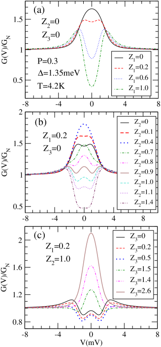
In Fig. 3, the calculated conductance spectra under three different barrier strengths are displayed in order to examine the influence of the barrier strength. We find from Fig. 3(a) that when the effect of charge inhomogeneity are not taken into account (i.e., and ), the normalized conductance at low bias decreases with increasing barrier strength and two peaks appear symmetrically about zero bias, like the previous BTK modelsBlonder ; Strijkers . This was already attributed to the suppression of Andreev reflection by the barrier strengthBlonder . In Fig. 3(b), it is shown how the evanescent Andreev reflection [through barrier strength (i.e. )] affect the conductance spectra. Clearly, the low-bias conductance would increase initially, with increasing , as shown by the curves with and , but, however, would decrease upon further increasing . From Eq. (7), we can infer that would reduce the effective barrier strength and hence increases the low-bias conductance. However, if is large, the effective barrier strength becomes negative. The negative potential barrier implies a potential well rather than a potential barrier. When the effective barrier strength becomes negative, the depth of the well increases with increasing and hence the conductance would be reduced by . Moreover, when the conductance increases with (i.e. the curves for and ), the dip at the zero-bias would diminish gradually and eventually a single peak occurs at zero bias (see the curve for ). The shape of conductance spectra for is similar to that of the curve in the clean regime (i.e. the curve for , shown in Fig. 3(a)). However, in comparison with the curves with no barrier, the height of the peak for is higher. The heights of peaks for and for no barrier are 1.81 and 1.67, respectively. In addition, we find that the peak for is sharper. We also notice that can generate double dips, like the curves for and .
In Fig. 3(c), the effect of the evanescent-quasiparticle-induced barrier strength is shown. In contrast with , would reduce the low-bias conductance first and then raise it. It is clear from Table I that the coefficient for and the approaches zero at high energy. Therefore, is insensitive to but may be influenced by . Similar to , for smaller , reduces the height of the barrier at high bias and hence increases and the low-bias normalized conductance decreases. For sufficiently large , a barrier is transformed into a well and decreases with . Hence, the normalized conductance could be enhanced by increasing . Furthermore, could raise zero-bias conductance above 2 (see the curve for ).
It is worth mentioning that, under the effect of charge inhomogeneity, the zero-bias normalized conductance does not reach its maximum in the clean limit. Indeed, the transmission of electrons into the superconductor should be obstructed by a barrier (or a well) especially upon Andreev reflection, as shown in Fig. 5 of ref. Blonder . Furthermore, at high bias, electrons propagate into the superconductor mainly through electron- and hole- like transmission and hence is independent of Andreev reflection probability. Therefore, the zero-bias conductance must decrease if is a constant. When and are included, the total barrier strength varies with voltage. Electrons may feel a higher barrier or a deeper well at high bias and therefore normalized conductance could increase in the presence of a barrier or a well.
IV.2 Anomalous spectra
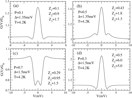
From the preceding section, we may conclude that the evanescent-hole-induced barrier strength could lead to zero-bias enhancement, sharp central peak, occurrence of dips while the evanescent-quasiparticle-induced barrier strength could substantially enhance the zero-bias conductance. By applying and , we can create the anomalous PCAR spectra for different spin polarizations, which are very similar to experimental observations, as shown in Fig. 4. In other words, all the observed anomalous characteristics can be reproduced in our model with suitable values of the various barrier strength parameters.
Fig. 4(a) shows the anomalous spectra with the dip structures. In experiments, the dips are usually located at Strijkers ; Sheet . The dips occur at mV in the present case. In the presence of the spreading resistance, the dips would move farther away from the central peak. This is consistent with the experimental observations. Fig. 4(b) and (c) show two different types of the ZBCP spectra. In Fig. 4(b), a higher conductance peak is located at zero bias and two small peaks appear symmetrically on both side of it, similar to the experimental results in ref. Geresdi . In Fig. 4(c), a zero-bias shallow hump appears at tunneling-like Andreev reflection spectra, similar to the experimental results in refs. Srikanth ; Kastalsky ; Magnee ; Quirion . The two ZBCP characteristics can both be obtained by adjusting , as shown in the curves for and of Fig. 3(b). Our results indicate that both dip structures and a ZBCP are due to the evanescent Andreev reflection. In ref. Srikanth , it was showed that the dip structures in the Andreev spectra [like Fig. 4(a)] could be transformed into the ZBCP [like Fig. 4(b)] by varying contact area, which is consistent with our results. Adjusting contact area could alter the properties of interface, , , , and and hence different types of the PCAR spectra would occur.
Fig. 4(d) shows both the dip structures and large zero-bias enhancement. In experiments, the dip structures are often accompanied by the large zero-bias enhancementShan ; Sheet . Our model can reproduce both the dip structures and large zero-bias enhancement. In addition, we find from Fig. 3(b) that the dips appear when reduces the zero-bias conductance. This indicates that the unusual zero-bias enhancement results from . In experiments, the dip structures, a ZBCP, and large zero-bias enhancement usually happen at large contact area (i.e. low resistance). Charge inhomgeneity is also pronounced for large contact area, as seen in Fig. 3(c). This supports the validity of our model. However, it should be noted that the increase of conductance with contact area is due to the increase of electron-transport channels instead of or . In the preceding subsection, it was illustrated how reduces and under the assumption of constant electron-transport channels. In principle, the charge inhomogeneity could also happen for the planar geometry. Therefore, our model could also be extended to the planar junctions.
IV.3 Temperature dependence of dip structures
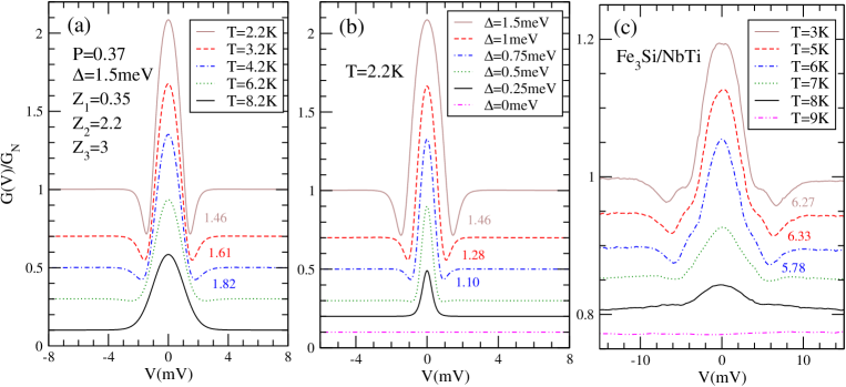
Let us now examine how the dip structures vary with temperature. The superconducting energy gap decreases with increasing temperatureTinkham . We plot the normalized conductance for different values of temperature and energy gap in Fig. 5(a) and Fig. 5(b), respectively. Fig. 5(a) indicates that the dips would be reduced gradually and also move away from the central peak as increases. Fig. 5(b) shows that, with decreasing , the dips would diminish gradually, too, but move towards the central peak. We can infer that the dips would disappear eventually when the temperature is raised. Moreover, from Fig. 2-2 in ref. Tinkham , near , the energy gap is almost insensitive to . If is larger, would decrease with more rapidly. When is increased up to the critical temperature , drops to zero. In other words, we predict that, with the temperature rising, the position of a dip should increase if temperature is low enough. Conversely, at higher temperatures, due to the rapid decrease of , the position of a dip could decrease with increasing temperature. Fig. 5(c) shows the measured temperature dependence of the dips for a Fe/Nb point contactSheet , which should correspond to the theoretical results in Fig. 5(b). Many other experimental works have shown the same temperature dependence of dip structures for a wide variety of combinations between metals and superconductorsNowack ; Mao ; Shan ; Gourgy ; Daghero . Furthermore, it was pointed out in the preceding subsection that dip structures and the ZBCP have the same physical origin. Therefore, indeed, the two local minima in the ZBCP spectra would be equivalent to the dip structures. Kastalsky et al. Kastalsky observed ZBCP spectra in the temperature range of K. Their data showed the two local minima in the conductance spectra moved to higher bias as temperature increased. Therefore, we infer that the dips may also move away from the central peak, as shown in Fig. 5(a).
IV.4 Fitting experimental spectra
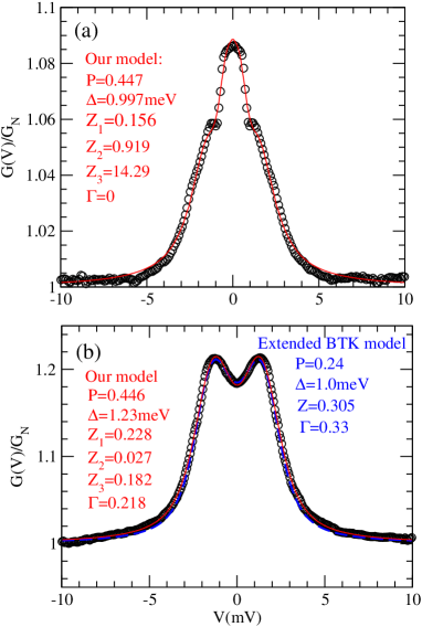
We performed the least squared fit to selected experimental data using our model and compared with the extended BTK model.Strijkers In addition to the , , , and , which are necessary in our model, , , and the extra resistance factor in Eq. (9) can also be used as fitting parameters to the experimental spectra. To minimize the fitting parameters, we chose to fit the measurements obtained from samples immersed in liquid Helium and fixed the temperature K. At first, superconducting energy gap for Pb was fixed at 1.23 meV and the was fixed at zero. If the fitting result was not satisfactory, we would turn on and/or as fitting parameters.
We find that, for small contact resistance ( ), a zero-bias conductance peak could appear in the experimental curve [Fig. 6(a)]. However, for large contact resistance ( ), we do not observe the ZBCP and an ordinary PCAR spectrum occurs, as shown in Fig. 6(b). We also find from Fig. 6(a) that, in contrast to the extended BTK modelStrijkers which could not reproduce the shoulder structures, our model could fit the ZBCP spectrum very well. Fig. 6(b) shows that our model also fits usual spectra well. Although the usual spectra could be fitted by the extended BTK modelStrijkers well, the resultant parameter is significantly smaller than that from the previous measurementsSoulen ; Nadgorny ; Paraskevopoulos ; Veerdonk . The spin polarization of permalloy has been determined by both PCARSoulen ; Nadgorny and spin-polarized tunnelingParaskevopoulos ; Veerdonk experiments, and was found to be in the range of 0.3-0.5. In our model, the fitted value of agrees well with these previous measurements. This indicates that, in our measurements, charge inhomogeneity may happen and, therefore, the extended BTK model could not explain the experimental data in Fig. 6(b).
V Conclusions
In conclusion, we have developed a modified 3-D BTK model by taking into account the effect of transport induced charge inhomogeneity on the barrier potential at ferromagnet-superconductor interfaces. To this end, we add two new parameters, namely, the evanescent hole-induced barrier strength and evanescent quasiparticle-induced barrier strength to describe the modified barrier strength. We find that would give rise to the dip structures and zero-bias conductance peak, while, on the other hand, would enhance the zero-bias conductance by decreasing the normal-state conductance . We have, therefore, offered a possible explanation for the anomalous conductance spectra which have been long standing problems in the field of PCAR spectroscopy. Furthermore, the results of our model fits to the experimental data have a good agreement with the measured ZBCP spectra as well as normal conductance spectra. Nevertheless, the standard -function form adopted here for the barrier potential at point contacts could be an oversimplication. Further theoretical and experimental works are certainly needed to fully understand these important issues in the PCAR spectroscopy.
Acknowledgments
The authors thank Hao-Chun Lee for valuable discussion. The authors also acknowledge financial supports from the National Science Council, Academia Sinica, and National Center for Theoretical Sciences of Taiwan as well as Center for Quantum Science and Engineering, National Taiwan University (CQSE-10R1004021).
References
- (1) S. K. Upadhyay, A. Palanisami, R. N. Louie, and R. A. Buhrman, Phys. Rev. Lett. 81, 3247 (1998).
- (2) R. J. Soulen, Jr., J. M. Byers, M. S. Osofsky, B. Nadgorny, T.Ambrose, S. F. Cheng, P. R. Broussard, C. T. Tanaka, J. Nowak, J. S. Moodera, A. Barry, and J. M. D. Coey, Science 282, 85 (1998).
- (3) Y. Ji, G. J. Strijkers, F. Y. Yang, J. M. Byers, A. Anguelouch, G. Xiao and C. L. Chien, Phys. Rev. Lett. 86, 5585 (2001).
- (4) A. F. Andreev, Sov. Phys. JETP 19, 1228 (1964).
- (5) G. E. Blonder, M. Tinkham, and T. M. Klapwijk, Phys. Rev. B 25, 4515 (1982).
- (6) G. J. Strijkers, Y. Ji, F. Y. Yang, C. L. Chien, and J. M. Byers, Phys. Rev. B 63, 104510 (2001).
- (7) A.A. Golubov, physica C 326-327,46 (1999).
- (8) P. Chalsani, S. K. Upadhyay, O. Ozatay, and R. A. Buhrman, Phys. Rev. B 75, 094417 (2007).
- (9) N. A. Mortensen, K. Flensberg, and A. P. Jauho, Phys. Rev. B 59, 10176 (1999).
- (10) I. I. Mazin, A. A. Golubov, and B. Nadgorny, J. Appl. Phys. 89, 7576 (2001).
- (11) A. Nowack, A. Heinz, F. Oster, D. Wohlleben, and G. Güntherodt, Phys. Rev. B 36, 2436 (1987).
- (12) H. Srikanth and A. K. Raychaudhuri, Phys. Rev. B 45, 383 (1992).
- (13) Y. DeWilde, J. Heil, A. G. M. Jansen, P. Wyder, R. Deltour, W. Assmus, A. Menovsky, W. Sun, and L. Taillefer, Phys. Rev. Lett. 72, 2278 (1994).
- (14) Y. DeWilde, N. Miyakawa, P. Guptasarma, M. Iavarone, L. Ozyuzer, J. F. Zasadzinski, P. Romano, D. G. Hinks, C. Kendziora, G. W. Crabtree, and K. E. Gray, Phys. Rev. Lett. 80, 153 (1998).
- (15) Ch. Wälti, H. R. Ott, Z. Fisk, and J. L. Smith, Phys. Rev. Lett. 84, 5616 (2000).
- (16) F. Laube, G. Goll, H. v. Lohneysen, M. Fogelstrom, and F. Lichtenberg, Phys. Rev. Lett. 84, 1595 (2000).
- (17) Z. Q. Mao, M. M. Rosario, K. D. Nelson, K. Wu, I. G. Deac, P. Schiffer, Y. Liu, T. He, K. A. Regan, and R. J. Cava, Phys. Rev. B 67, 094502 (2003).
- (18) S. Hacohen-Gourgy, B. Almog, and G. Deutscher, Appl. Phys. Lett. 92, 152502 (2008).
- (19) D. Daghero and R. S. Gonnelli, Supercond. Sci. Technol. 23, 043001 (2010).
- (20) A. Kastalsky, A. W. Kleinsasser, L. H. Greene, R. Bhat, F. P. Milliken, and J. P. Harbison, Phys. Rev. Lett. 67, 3026 (1991).
- (21) P. H. C. Magnée, N. van der Post, P. H. M. Kooistra, B. J. van Wees, and T. M. Klapwijk, Phys. Rev. B 50, 4594 (1994).
- (22) D. Quirion, C. Hoffmann, F. Lefloch, and M. Sanquer, Phy. Rev. B 65, 100508(R) (2002).
- (23) L. Shan, H. J. Tao, H. Gao, Z. A. Ren, G. C. Che, and H. H. Wen, Phy. Rev. B 68, 144510 (2003).
- (24) G. Sheet, S. Mukhopadhyay, and P. Raychaudhuri, Phy. Rev. B 69, 134507 (2004).
- (25) H. Schmidt, J. F. Zasadzinski, K. E. Gray, and D. G. Hinks, Phys. Rev. Lett. 88, 127002 (2002).
- (26) A. Geresdi, A. Halbritter, M. Csontos, Sz. Csonka, G. Mihály, T. Wojtowicz, X. Liu, B. Janko, and J. K. Furdyna, Phys. Rev. B 77, 233304 (2008); A. Geresdi, A. Halbritter, and G. Mihály, Phys. Rev. B 82, 212501 (2010).
- (27) Y. Tanaka and S. Kashiwaya, Phys. Rev. Lett. 24, 3451 (1995); S. Kashiwaya, Y. Tanaka, M. Koyanagi, H. Takashima, and K. Kajimura, Phys. Rev. B 51, 1350 (1995); S. Kashiwaya and Y. Tanaka, Rep. Prog. Phys. 63, 1641 (2000).
- (28) Y. Tanaka, M. Sato, and N. Nagosa, J. Phys. Soc. Jpn. 81, 011013 (2010).
- (29) C. H. Kant, O. Kurnosikov, A. T. Filip, P. LeClair, H. J. M. Swagten, and W. J. M.de Jonge, Phys. Rev. B 66, 212403 (2002).
- (30) N. Auth, G. Jakob, T. Block, and C. Felser, Phys. Rev. B 68, 024403 (2003).
- (31) Y. Bugoslavsky, Y. Miyoshi, S. K. Clowes, W. R. Branford, M. Lake, I. Brown, A. D. Caplin, and L. F. Cohen, Phys. Rev. B 71, 104523 (2005).
- (32) V. Baltz, A D Naylor, K. M. Seemann, W. Elder, S. Sheen, K. Westerholt, H. Zabel, G. Burnell, C. H. Marrows and B J Hickey, J. Phys.: Condens. Matter 21, 095701 (2009).
- (33) G. T. Woods, R. J. Soulen, Jr., I. I. Mazin, B. Nadgorny, M. S. Osofsky, J. Sanders, H. Srikanth, W. F. Egelhoff, and R. Datla, Phys. Rev. B 70, 054416 (2004).
- (34) T. W. Chiang, Y. H. Chiu, S. Y. Huang, S. F. Lee, J. J. Liang, H. Jaffres, J. M. George, and A. Lemaitre, J. Appl. Phys. 105, 07C507 (2009).
- (35) T. Y. Chen, S. X. Huang, and C. L. Chien, Phys. Rev. B 81, 214444 (2010).
- (36) S. Kashiwaya, Y. Tanaka, N. Yoshida, and M. R. Beasley, Phys. Rev. B 60, 3572 (1999).
- (37) C. W. J. Beenakker, Phys. Rev. Lett. 97, 067007 (2006).
- (38) Y. F. Hsu and G. Y. Guo, Phys. Rev. B 81, 045412 (2010).
- (39) M. I. Katsnelson, arXiv:1101.2542v1 (2011).
- (40) B. K. Nikolić, J. K. Freericks, and P. Miller, Phys. Rev. B 65, 064529 (2002).
- (41) J. D. Jackson, Classical Electrodynamics (Wiley, Hoboken, 1999), Chap. 1.
- (42) Low Level Measurements Handbook, 6th ed. (Keithley Instruments Inc., Cleveland, 2004).
- (43) B. K. Nikolić and P. B. Allen, Phys. Rev. B 60, 3963 (1999).
- (44) M. Tinkham, Introduction to Superconductivity (McGraw-Hill, New York, 1975), Chap. 2.
- (45) B. Nadgorny, R. J. Soulen, Jr., M. S. Osofsky, I. I. Mazin, G. Laprade, R. J. M. van de Veerdonk, A. A. Smits, S. F. Cheng, E. F. Skelton, and S. B. Qadri, Phys. Rev. B 61, R3788 (2000).
- (46) D. Paraskevopoulos, R. Meservey, and P. M. Tedrow, Phys. Rev. B 16, 4907 (1977).
- (47) R. J. M. van de Veerdonk, J. S. Moodera, and W. J. M. de Jonge, in 15th ICMFS Conf. Digests (1997), pp. 74-75.