Magnetic-field-dependent photodynamics of single NV defects in diamond: Application to qualitative all-optical magnetic imaging
Abstract
Magnetometry and magnetic imaging with nitrogen-vacancy (NV) defects in diamond rely on the optical detection of electron spin resonance (ESR). However, this technique is inherently limited to magnetic fields that are weak enough to avoid electron spin mixing. Here we focus on the high off-axis magnetic field regime for which spin mixing alters the NV defect spin dynamics. We first study in a quantitative manner the dependence of the NV defect optical properties on the magnetic field vector B. Magnetic-field-dependent time-resolved photoluminescence (PL) measurements are compared to a seven-level model of the NV defect that accounts for field-induced spin mixing. The model reproduces the decreases in (i) ESR contrast, (ii) PL intensity and (iii) excited level lifetime with an increasing off-axis magnetic field. We next demonstrate that those effects can be used to perform all-optical imaging of the magnetic field component orthogonal to the NV defect axis. Using a scanning NV defect microscope, we map the stray field of a magnetic hard disk through both PL and fluorescence lifetime imaging. This all-optical method for high magnetic field imaging at the nanoscale might be of interest in the field of nanomagnetism, where samples producing fields in excess of several tens of milliteslas are typically found.
1 Introduction
The nitrogen-vacancy (NV) defect in diamond is a solid-state quantum system that has been extensively studied over the last years [1]. Potential applications include quantum information processing [2, 3, 4, 5], imaging in life science [6], hybrid quantum systems [7, 8, 9] and magnetic sensing and imaging [10, 11, 12, 13]. For the latter application, the magnetic field is evaluated by measuring the Zeeman shifts of the NV defect electron spin sublevels through the optical detection of electron spin resonance (ESR). The main advantage of NV-based magnetometry is the possible combination of atomic-scale spatial resolution with high magnetic field sensitivity – below 10 nT/Hz1/2 [14] – even under ambient conditions. Magnetic imaging with diffraction-limited micrometer resolution has been demonstrated using an ensemble of NV defects [15, 16, 17] while recent experiments have reached the nanoscale with a single NV defect coupled to a scanning probe microscope [13, 18, 19].
However, ESR-based magnetometry with NV defects is intrinsically limited to magnetic fields with an amplitude and an orientation such that the electron spin quantization axis remains fixed by the NV defect axis itself. Indeed, any significant spin mixing induced by an off-axis magnetic field rapidly reduces the contrast of optically-detected ESR spectra because optically induced spin polarization and spin dependent photoluminescence (PL) of the NV defect become inefficient. Besides a decreased ESR contrast, the PL intensity as well as the effective excited level lifetime are observed to decrease with an increasing off-axis magnetic field [22, 23]. It was recently shown that this property can be used as a resource to perform all-optical magnetic field mapping with a scanning NV defect [18, 19]. The purpose of the present work is to study in a quantitative manner the dependence of the NV defect optical properties on the magnetic field vector B, and to discuss the implications for magnetic field imaging. The paper is organized as follows. In Section 2, we first investigate the dynamics of optically-pumped NV defects as a function of B, focusing on (i) the ESR contrast, (ii) the PL intensity and (iii) the excited level lifetime. A simple seven-level model of the NV defect is developed and compared to magnetic-field-dependent time-resolved PL measurements. This method provides a simple way to extract all relevant photophysical parameters of the NV defect and compute its optical response as a function of the field. The results of the calculation are then compared to single site measurements and discussed in the context of magnetic field imaging. In Section 3, we report on experiments of all-optical magnetic imaging in the high off-axis magnetic field regime using a scanning NV defect microscope. In particular, fluorescence lifetime imaging (FLIM) capabilities allows us to record not only PL images but also lifetime ones, a feature that could reveal useful beyond magnetic imaging, e.g. for mapping the local density of electromagnetic states (LDOS) of photonic nanostructures [20, 21].
2 Photodynamics of single NV defects in a static magnetic field
2.1 Model
The negatively charged NV defect in diamond consists of a substitutional nitrogen atom (N) associated with a vacancy (V) in an adjacent lattice site of the diamond matrix, giving a defect with symmetry (Fig. 1(a)). Its ground level is a spin triplet , whose degeneracy is lifted by spin-spin interaction into a singlet state of spin projection and a doublet , separated by GHz in the absence of magnetic field [24]. Here, denotes the spin projection along the NV defect axis (Fig. 1(a)). When a magnetic field is applied to the defect, the ground level spin Hamiltonian reads
| (1) |
with and , where is the Planck constant, is the Bohr magneton, and is the electron -factor. We note that strain-induced splitting and hyperfine interaction with nearby nuclear spins are neglected in Eq. (1). In zero field, the quantization axis is thus fixed by the NV defect axis and the eigenstates are labelled , and , corresponding to spin projections , and , respectively (Fig. 1(b)).
The defect can be optically excited through a dipole-allowed transition to a excited level, which is also a spin triplet. Besides, the excited level is an orbital doublet which is averaged at room temperature [25, 26] leading to a zero-field splitting GHz with the same quantization axis and similar gyromagnetic ratio as in the ground level [27, 28]. The excited level spin Hamiltonian is thus simply given by Eq. (1) while replacing by . The excited level eigenstates in zero field are labelled , and , corresponding to spin projections , and , respectively (Fig. 1(b)). Once optically excited in the level, the NV defect can relax either through the same radiative transition producing a broadband red photoluminescence (PL), or through a secondary path involving non radiative intersystem crossing (ISC) to singlet states. Recent experiments have identified two singlet states (,) [29, 30], whereas theoretical studies predict the presence of a third singlet state between the ground and excited triplet levels [31]. In the present work, the singlet states are summarized into a single ‘metastable’ level labelled . Spin-dependent ISC from the level to the ‘metastable’ level is responsible for efficient spin-polarization in the spin sublevel through optical pumping as well as for spin-dependent PL of the NV defect. These two properties enable the detection of electron spin resonance (ESR) on a single NV defect by optical means [32].
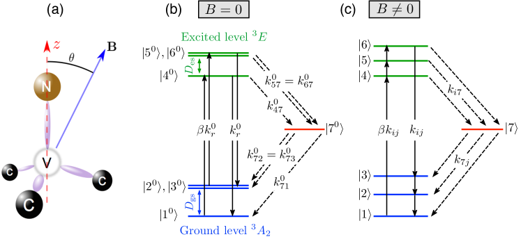
Within this seven-level model of the NV defect, the zero-field transition rate from to is denoted by . We consider that optical transitions are purely spin-conserving, and that the radiative relaxation rate is spin-independent, i.e. . This is reasonable since Robledo et al. recently determined that spin-flip radiative transition rates are at most of their spin-conserving counterpart [33]. On the other hand, the optical pumping rates from the ground to the excited level are proportional to the corresponding relaxation rates through for and , where is the optical pumping parameter. Lastly, ISC transition rates at zero-field only depend on the absolute value of , i.e. and . Following these assumptions, there are five intrinsic parameters left in the system, namely , , , and , and an extrinsic parameter linked to the optical pumping power (Fig. 1(b)).
When a static magnetic field is applied to the NV defect (Fig. 1(c)), the seven eigenstates of the system can be expressed as linear combinations of the zero-field eigenstates
| (2) |
where the coefficients are numerically computed by using the expressions of and , and given that . The new transition rates are then related to the zero-field transition rates through the transformation
| (3) |
which represents a statistical averaging using the weights of the initial and the final state of the transition. The lifetime of each eigenstate in the excited level is then given by with .
With the aim of studying the time-resolved optical response of a single NV defect placed in a static magnetic field, we consider a pulsed optical excitation with a pulse duration and a repetition period such that . After optical excitation (), each excited state population decays exponentially as once averaged over many excitation cycles. The rate of emitted photons from state is the radiative part of the total decay and reads . The detected time-resolved PL signal is thus finally obtained by summing over the three excited states
| (4) |
where is the collection efficiency. In this equation, the magnetic field dependent transition rates are given by Eq. (3) and the set of coefficients are inferred by solving the classical rate equations of the system
| (5) |
while considering a closed seven-level model, i.e. , and the periodic condition . The detected time-resolved PL signal is therefore given by a tri-exponential decay, where the amplitude and the lifetime of each component is expressed as a function of the zero-field transition rates and the optical pumping parameter . We expect that at low magnetic field owing to efficient spin polarization of the NV defect in by optical pumping, while those populations are balanced in the limit of strong transverse magnetic fields.
Finally, we infer the contrast of optically-detected ESR spectra for a single NV defect placed in a static magnetic field. For that purpose, non-vanishing transition rates (resp. ) are added in the model to account for a microwave field in resonance with the (resp. ) electron spin transition in the ground level. In the following ESR spectra are recorded with continuous-wave (CW) optical excitation. In this case, the mean PL rate is given by where the averaged populations are inferred by solving the classical rate equations (Eq. (5)) at the steady state. In this framework, the ESR contrast of the transition is defined by
| (6) |
where (resp. ) denotes the NV defect PL rate without applying the microwave field (resp. with a resonant microwave field). A similar expression holds for the transition.
2.2 Experimental setup
Individual NV defects hosted in a high-purity type IIa diamond crystal (Element Six) are optically isolated at room temperature using a scanning confocal microscope. Optical excitation at nm wavelength is provided either by a CW laser or by a pulsed laser with a pulse duration ps and a MHz repetition rate (PicoQuant, LDH-P-FA-530B). The detection system comprises a confocal arrangement, an avalanche photodiode working in the single-photon counting regime (Perkin-Elmer, SPCM-AQR-14), and a time-correlated single-photon counting module with a bin size of ps (PicoQuant, PicoHarp 300). An electromagnet is used to apply a static magnetic field with controlled amplitude, while ESR transitions in the ground level are driven with a microwave field applied through a copper microwire directly spanned on the diamond surface.
2.3 Results and discussion
For each studied NV defect, the angle between its symmetry axis () and the magnetic field was first measured by using ESR spectroscopy (see Tab. 1). For that purpose, optically-detected ESR spectra were recorded by sweeping the frequency of a microwave field while monitoring the NV defect PL intensity. Owing to spin dependent PL, two dips can be observed in the PL signal, corresponding to electron spin transitions and (Fig. 2(a)). Measuring the electron spin transition frequencies as a function of the magnetic field amplitude allows us to extract the angle through data fitting with the eigenenergies of the ground level spin Hamiltonian (Fig. 2(b)) [13].
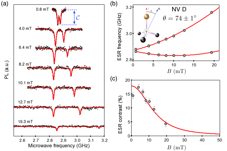
The ESR spectra depicted in Figure 2(a) can also be used to estimate the ESR contrast as a function of the magnetic field amplitude (Fig. 2(c)). If the magnetic field is such that (see Eq. (1)), the quantization axis is fixed by the NV defect axis, and a high ESR contrast is observed. Conversely, when the condition is not fulfilled, the quantization axis is rather determined by the applied magnetic field and is no longer a good quantum number. The eigenstates of the spin Hamiltonian are then given by superpositions of the and spin sublevels, both in the ground and excited levels (see Eq. (2)). As a result, optically-induced spin polarization and spin-dependent PL of the NV defect become inefficient, and the contrast of optically detected ESR vanishes, as shown in Figure 2(c). Magnetic field imaging through optically-detected ESR is therefore inefficient in the regime of ‘high’ off-axis magnetic field. Nevertheless, the NV defect optical response can be used to extract information about the magnetic field in this regime, as explained below.
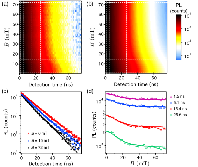
The photophysical parameters of the NV defect were first measured in order to compute its optical response as a function of the field. For that purpose, time-resolved PL traces were recorded while increasing the magnetic field amplitude for a given angle , as shown in Figure 3(a). Fitting the whole set of data with Eq. (4) allows us to extract the zero-field transition rates as well as the normalization coefficient and optical pumping parameter (Fig. 3(b)). Horizontal and vertical linecuts of the matrix are plotted in Figure 3(c) and (d), respectively, showing good agreement between the experimental data and the model. We emphasize the fact that such a tri-exponential fit can be reliably applied because all traces are fitted at once. We thus benefit from the correlations between traces at different magnetic field amplitudes, whereas each trace taken individually could not be fitted satisfactorily with a tri-exponential function. The transition rates extracted from the fitting procedure are summarized in Table 1 for four different NV defects oriented with different angles with respect to the magnetic field. We note that these values are in agreement with those reported in Ref. [33], which were obtained using a different approach based on multi-pulse excitation techniques combined with coherent electron spin manipulation. As expected, we measure a spin-dependent ISC rate , which is responsible for optically-induced spin polarization and spin-dependent PL response of the NV defect. Furthermore, our measurements seem to confirm that the metastable state decays roughly as often in the state as in the state, i.e. [33], in contradiction with the initial belief in a coupling to alone [24].
| NV C | NV D | NV E | NV F | |
|---|---|---|---|---|
| s | ||||
| s | ||||
| s | ||||
| s | ||||
| s |
Having completely characterized the NV defect and extracted its photophysical parameters, we now discuss the dependence of the NV defect optical properties on the field and its application for magnetic field imaging. Figure 4(a) shows the normalized PL intensity calculated using the seven-level model with the parameters of NV E as a function of and , varied in the range 0-150 mT. Regardless of the value of in this range, the PL steadily decreases with an increasing , with a PL drop exceeding for mT. This effect results from a mixing of electron spin states both in the ground and excited levels, which enhances the probability of non-radiative ISC to the metastable level and reduces the PL intensity. We note that in the low transverse field regime, the PL intensity also exhibits the well-known sharp drops at mT and at mT, corresponding to spin mixing induced by a level anti-crossing within the excited and ground level, respectively [22, 25]. In Figure 4(c), the normalized integrated PL signal is plotted as a function of for three distinct NV defects, oriented with different angles with respect to B. The data are well reproduced by the model (solid lines) without any free parameters. This graph highlights the fact that the monotonous PL decrease with is a general feature of NV defects, occurring whenever B is not aligned with to better than (see Fig. 4(a)). Such a PL drop can be used to discriminate between low and high transverse magnetic field regions. Although not fully quantitative, a PL measurement sets a lower bound to the magnetic field amplitude. For instance one deduces from the contour lines in Fig. 4(a) that a PL drop of 30% implies that the field has an amplitude mT. This property can be used to develop a microscope capable of qualitatively mapping large magnetic field regions at the nanoscale. We note that this method could be used with any solid-state emitter exhibiting spin-dependent PL [34], with a characteristic magnetic field range given by its zero-field splitting (Eq. (1)).
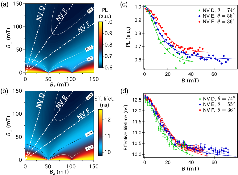
The PL drop induced by spin mixing is correlated with a reduction of the effective lifetime of the NV defect excited level (Fig. 3(c)), which is defined as the exponential decay constant that best fit a given time-resolved PL trace. Using the photophysical parameters of NV E, we infer the effective lifetime as a function of and by fitting the time-resolved PL traces calculated from the seven-level model with a single exponential decay. As shown in Figure 4(b), the evolution of as a function of the magnetic field is clearly correlated with the PL rate (Fig. 4(a)). This feature illustrates that field-induced spin level mixing increases the mean probability for non radiative ISC transitions to the metastable level, which not only decreases the PL rate but also increases the decay rate from the excited level, thus leading to an overall reduction of the excited level lifetime. In Figure 4(d), is plotted as a function of for three different defects, together with the model that introduces no free parameters. In the same way as for the PL rate measurement, knowing the effective lifetime sets a lower bound for the amplitude of the magnetic field (see contour lines in Fig. 4(b)), and can be used to map high off-axis magnetic field regions, as demonstrated in the next section.
3 All-optical magnetic field imaging with a scanning NV defect
Magnetic field imaging with a scanning NV defect is performed with the experimental setup depicted in Figure 5(a), which combines an optical confocal microscope and a customized tuning-fork-based atomic force microscope (Attocube Systems, CFM/AFM), all operating under ambient conditions. A 20-nm diamond nanocrystal hosting a single NV defect is first grafted at the end of the AFM tip following the procedure described in Refs.[19, 35]. A confocal microscope placed on top of the tip allows us both to excite and collect the NV defect magnetic-field-dependent PL. The unicity of the emitter placed at the apex of the AFM tip was checked by measuring in pulsed regime the histogram of time delays between two consecutive single-photon detections with a Hanbury Brown and Twiss interferometer. As shown in Figure 5(b), a strong reduction of coincidences is observed around zero delay, which is the signature that a single NV defect is attached to the tip [36].
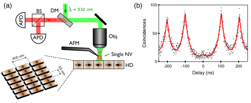
As a test sample, we used a piece of a commercial magnetic hard disk composed of nm x nm bits with random in-plane magnetization (Fig. 5(a)). Two adjacent magnetic bits with opposite magnetizations produce a stray field coming in or out at the boundary between the two bits. Imaging such a stray field is performed by recording the NV defect PL intensity while scanning the magnetic hard disk. In this experiment, the AFM is operated in tapping mode in order to maintain the mean probe-to-sample distance to a constant value. As shown in Figure 6(a), the PL image reveals an array of dark areas that correspond to regions of high transverse magnetic field. Such dark areas indicate magnetization reversals, very much like in magnetic force microscopy (MFM) measurements with the difference that in addition MFM distinguishes between fields coming in or out of the sample, corresponding to repulsive or attractive forces. The distance between two consecutive dark lines is measured to be larger than 100 nm in Figure 6(a). For instance, it is approximately nm in the zoom shown in Figure 6(c), which corresponds to the size of two magnetic bits. We therefore believe that in this particular experiment, at least two consecutive bits with the same magnetization are needed in order to build up a stray field that is strong enough to induce a detectable PL quenching.
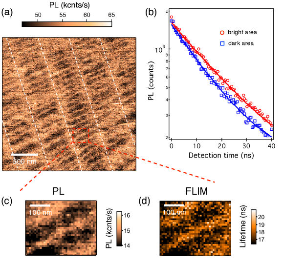
As discussed in Section 2, the field-induced PL quenching is associated with an overall reduction of the NV defect excited-level lifetime. This is illustrated in Figure 6(b), which shows PL decay traces measured when the tip stands either on a bright area (low magnetic field) or on a dark area (high transverse magnetic field). Single exponential data fits give effective lifetimes ns and ns, corresponding to a reduction of . We note that the lifetime of the NV defect is larger in nanocrystals compared to bulk measurements reported in Figure 4(b)), owing to change of the surrounding refractive index [37]. By recording PL decay traces while scanning the sample, magnetic field mapping can also be achieved through fluorescence lifetime imaging (FLIM), as shown in Figure 6(d)). As expected, FLIM and PL images are clearly correlated: the regions of low effective lifetime closely match those of low PL signal, in correspondence to regions of high off-axis magnetic field (Fig. 6(c)-(d)).
The maximum PL contrast in Fig. 6(b) is about 30%, which is close to what was measured for NV defects in bulk diamond. As discussed in Section 2, measuring the normalized PL intensity can in principle give access to a lower bound for provided that one knows all relevant parameters of the experiment, including the transition rates of the NV defect employed. However, those are affected by the electromagnetic environment of the NV defect – proximity to the AFM tip, to the metallic sample, etc. – and are therefore not readily accessible. Assuming that the general behavior of Figure 4(a) is however still approximately valid here, one can state that the dark regions in Figure 6(a) correspond to a magnetic field exceeding mT. This would be consistent with the stray field expected for such a magnetic hard disk at a distance of a few tens of nanometers [19]. Although not quantitative, all optical magnetic field imaging with a scanning NV defect is thus a relatively simple way to map regions of magnetic field larger than a few tens of mT at the nanoscale. Furthermore, unlike MFM whose magnetic tip is likely to perturb the magnetization of the studied sample, the NV defect probe introduces no magnetic back action to the sample at first order.
Finally, we note that the ability to perform fluorescence lifetime imaging (FLIM) with a scanning NV defect opens up a large range of possibilities in the field of nanophotonics. Indeed, mapping the local density of electromagnetic states (LDOS) above non-magnetic samples is in reach, with the potential for vectorial LDOS mapping if one uses NV defects with different orientations. Compared to recent demonstrations of scanning FLIM [20, 21], advantages of NV defects are their perfect photostability as well as their atomic-sized spatial resolution. In this context, this work is a starting-point for understanding and quantifying the relation between the NV defect dynamics and the LDOS, a necessary step for future LDOS mapping experiments.
4 Conclusion
In this article the optical properties of NV defects in diamond have been studied as a function of the external magnetic field. We performed time-resolved measurements and developed a seven-level model that accounts for the decreased ESR contrast, PL intensity and effective lifetime when a transverse magnetic field is applied. We demonstrated an application of those effects to nanoscale magnetic imaging. Using a scanning NV defect microscope, we mapped the stray field of a magnetic hard disk by recording either PL or lifetime images. This all-optical method for high magnetic field imaging might be of interest in the field of nanomagnetism, where samples producing fields in excess of several tens of milliteslas are typical.
Acknowledgments
The authors acknowledge A. Dréau, L. Mayer, F. Grosshans, S. Rohart, and A. Thiaville for fruitful discussions. This work was supported by the Agence Nationale de la Recherche (ANR) through the projects Diamag and Advice, by C’Nano Ile-de-France and by RTRA-Triangle de la Physique (contract 2008-057T).
References
References
- [1] Jelezko F and Wrachtrup J 2006 Single defect centres in diamond: A review Phys. Stat. Sol. (a) 203 3207
- [2] Gurudev Dutt M V, Childress L, Jiang L, Togan E, Maze J, Jelezko F, Zibrov A S, Hemmer P R and Lukin M D 2007 Quantum register based on individual electronic and nuclear spin qubits in diamond Science 316 1312
- [3] Neumann P, Kolesov R, Naydenov B, Beck J, Rempp F, Steiner M, Jacques V, Balasubramanian G, Markham M L, Twitchen D J, Pezzagna S, Meijer J, Twamley J, Jelezko F and Wrachtrup J 2010 Quantum register based on coupled electron spins in a room-temperature solid Nat. Phys. 6 249
- [4] Robledo L, Childress L, Bernien H, Hensen B, Alkemade P F A and Hanson R 2011 High-fidelity projective read-out of a solid-state spin quantum register Nature 477 574
- [5] Fuchs G D, Burkard G, Klimov P V and Awschalom D D 2011 A quantum memory intrinsic to single nitrogen-vacancy centres in diamond Nat. Phys. 7 789
- [6] McGuinness L P, Yan Y, Stacey A, Simpson D A, Hall L T, Maclaurin D, Prawer S, Mulvaney P, Wrachtrup J, Caruso F, Scholten R E and Hollenberg L C L 2011 Quantum measurement and orientation tracking of fluorescent nanodiamonds inside living cells Nat. Nanotechnol. 6, 358
- [7] Kubo Y, Grezes C, Dewes A, Umeda T, Isoya J, Sumiya H, Morishita N, Abe H, Onoda S, Ohshima T, Jacques V, Dreau A, Roch J-F, Diniz I, Auffeves A, Vion D, Esteve D and Bertet P 2011 Hybrid quantum circuit with a superconducting qubit coupled to a spin ensemble Phys. Rev. Lett. 107 220501
- [8] Arcizet O, Jacques V, Siria A, Poncharal P, Vincent P and Seidelin S 2011 A single nitrogen-vacancy defect coupled to a nanomechanical oscillator Nat. Phys. 7 879
- [9] Kolkowitz S, Bleszynski Jayich A C, Unterreithmeier Q P, Bennett S D, Rabl P, Harris J G E and Lukin M D 2012 Coherent Sensing of a Mechanical Resonator with a Single-Spin Qubit Science 335 1603
- [10] Degen C 2008 Scanning magnetic field microscope with a diamond single-spin sensor Appl. Phys. Lett. 92 243111
- [11] Taylor J M, Cappellaro P, Childress L, Jiang L, Budker D, Hemmer P R, Yacobi A, Walsworth R and Lukin M D 2008 High-sensitivity diamond magnetometer with nanoscale resolution Nat. Phys. 4 810
- [12] Maze J R, Stanwix P L, Hodges J S, Hong S, Taylor J M, Cappellaro P, Jiang L, Gurudev Dutt M V, Togan E, Zibrov A S, Yacoby A, Walsworth R L and Lukin M D 2008 Nanoscale magnetic sensing with an individual electronic spin in diamond Nature 455 644
- [13] Balasubramanian G, Chan I Y, Kolesov R, Al-Hmoud M, Tisler J, Shin C, Kim C, Wojcik A, Hemmer P R, Krueger A, Hanke T, Leitenstorfer A, Bratschitsch R, Jelezko F and Wrachtrup J 2008 Nanoscale imaging magnetometry with diamond spins under ambient conditions Nature 455 648
- [14] Balasubramanian G, Neumann P, Twitchen D, Markham M, Kolesov R, Mizuochi N, Isoya J, Achard J, Beck J, Tissler J, Jacques V, Hemmer P R, Jelezko F and Wrachtrup J 2009 Ultralong spin coherence time in isotopically engineered diamond Nature Mater. 8 383
- [15] Maertz B J, Wijnheijmer A P, Fuchs G D, Nowakowski M E and Awschalom D D 2010 Vector magnetic field microscopy using nitrogen vacancy centers in diamond Appl. Phys. Lett. 96 092504
- [16] Steinert S, Dolde F, Neumann P, Aird A, Naydenov B, Balasubramanian G, Jelezko F and Wrachtrup J 2010 High sensitivity magnetic imaging using an array of spins in diamond Rev. Sci. Instr. 81 043705
- [17] Pham L M, Le Sage D, Stanwix P L, Yeung T K, Glenn D, Trifonov A, Cappellaro P, Hemmer P R, Lukin M D, Park H, Yacoby A and Walsworth R L 2011 Magnetic field imaging with nitrogen-vacancy ensembles New J. Phys. 13 045021
- [18] Maletinsky P, Hong S, Grinolds M S, Hausmann B, Lukin M D, Walsworth R-L, Loncar M and Yacoby A 2012 A robust scanning diamond sensor for nanoscale imaging with single nitrogen-vacancy centres Nat. Nano. 7 320
- [19] Rondin L, Tetienne J-P, Spinicelli P, Dal Savio C, Karrai K, Dantelle G, Thiaville A, Rohart S, Roch J-F and Jacques V 2012 Nanoscale magnetic field mapping with a single spin scanning probe magnetometer Appl. Phys. Lett. 100 153118
- [20] Farahani J N, Pohl D W, Eisler H-J and Hecht B 2005 Single Quantum Dot Coupled to a Scanning Optical Antenna: A Tunable Superemitter Phys. Rev. Lett. 95 017402
- [21] Frimmer M, Chen Y and Koenderink A F 2011 Scanning Emitter Lifetime Imaging Microscopy for Spontaneous Emission Control Phys. Rev. Lett. 107 123602
- [22] Epstein R J, Mendoza F M, Kato Y K, Awschalom D D 2005 Anisotropic interactions of a single spin and dark-spin spectroscopy in diamond Nat. Phys. 1 94
- [23] Lai N D, Zheng D, Jelezko F, Treussart F, Roch J-F 2009 Influence of a static magnetic field on the photoluminescence of an ensemble of nitrogen-vacancy color centers in a diamond single-crystal Appl. Phys. Lett. 95 133101
- [24] Manson N B, Harrison J P, Sellars M J 2006 Nitrogen-vacancy center in diamond: model of the electronic structure and associated dynamics Phys. Rev. B 74 104303
- [25] Rogers L J, McMurtrie R L, Sellars M J and Manson N B 2009 Time-averaging within the excited state of the nitrogen-vacancy centre in diamond New J. Phys. 11 063007
- [26] Batalov A, Jacques V, Kaiser F, Siyushev P, Neumann P, Rogers L J, McMurtrie R L, Manson N B, Jelezko F and Wrachtrup J 2009 Low Temperature Studies of the Excited-State Structure of Negatively Charged Nitrogen-Vacancy Color Centers in Diamond Phys. Rev. Lett. 102 195506
- [27] Fuchs G D, Dobrovitski V V, Hanson R, Batra A, Weis C D, Schenkel T and Awschalom D D 2008 Excited-state spectroscopy using single spin manipulation in diamond Phys. Rev. Lett. 101 117601
- [28] Neumann P, Kolesov R, Jacques V, Beck J, Tisler J, Batalov A, Rogers L, Manson N B, Balasubramanian G, Jelezko F and Wrachtrup J 2009 Excited-state spectroscopy of single NV defects in diamond using optically detected magnetic resonance New J. Phys. 11 013017
- [29] Rogers L J, Armstrong S, Sellars M J and Manson N B 2008 Infrared emission of the NV centre in diamond: Zeeman and uniaxial stress studies New J. Phys. 10 103024
- [30] Acosta V M, Jarmola A, Bauch E and Budker D 2010 Optical properties of the nitrogen-vacancy singlet levels in diamond Phys. Rev. B 82 201202(R)
- [31] Ma Y, Rohlfing M and Gali A 2010 Excited states of the negatively charged nitrogen-vacancy color center in diamond Phys. Rev. B 81 041204
- [32] Gruber A, Drbenstedt A, Tietz C, Fleury L, Wrachtrup J and von Borczyskowski C 1997 Scanning confocal optical microscopy and magnetic resonance on single defect centres Science 276 2012
- [33] Robledo L, Bernien H, van der Sar T and Hanson R 2011 Spin dynamics in the optical cycle of single nitrogen-vacancy centres in diamond New J. Phys. 13 025013
- [34] Koehl W F, Buckley B B, Heremans F J, Calusine G and Awschalom D D 2011 Room temperature coherent control of defect spin qubits in silicon carbide Nature 479, 84
- [35] Cuche A, Drezet A, Sonnefraud Y, Faklaris O, Treussart F, Roch J-F and Huant S 2009 Near-field optical microscopy with a nanodiamond-based single-photon tip Opt. Exp. 17 19969
- [36] Lounis B and Moerner W E 2000 Single photons on demand from a single molecule at room temperature Nature 407, 491
- [37] Beveratos A, Brouri R, Gacoin T, Poizat J-P and Grangier P 2001 Nonclassical radiation from diamond nanocrystals Phys. Rev A 64 061802R