Thermoelectric transport in strained Si and Si/Ge heterostructures
Abstract
The anisotropic thermoelectric transport properties of bulk silicon strained in [111]-direction were studied by detailed first-principles calculations focussing on a possible enhancement of the power factor. Electron as well as hole doping were examined in a broad doping and temperature range. At low temperature and low doping an enhancement of the power factor was obtained for compressive and tensile strain in the electron-doped case and for compressive strain in the hole-doped case. For the thermoelectrically more important high temperature and high doping regime a slight enhancement of the power factor was only found under small compressive strain with the power factor overall being robust against applied strain. To extend our findings the anisotropic thermoelectric transport of an [111]-oriented Si/Ge superlattice was investigated. Here, the cross-plane power factor under hole-doping was drastically suppressed due to quantum-well effects, while under electron-doping an enhanced power factor was found. With that, we state a figure of merit of ZT and ZT at and for the electron-doped [111]-oriented Si/Ge superlattice. All results are discussed in terms of band structure features.
pacs:
31.15.A-,71.15.Mb,72.20.Pa,72.20.-i,68.65.Cd1 Introduction
Thermoelectric phenomena were first described for metals by Seebeck at the beginning of the 19th century and revived by Ioffe in the late 1950’s by the introduction of semiconductors to thermoelectric devices [1, 2]. However, since then thermoelectrics were restricted to a scientific and economic niche mainly due to their poor conversion efficiency [3, 4]. Nowadays emerging global need for energy production and conservation has intensified interest and research in more effective alternative energy technologies to reduce our dependence on fossil fuels. Contributing to this, thermoelectric devices could partially convert wasted heat into electricity by their ability to transform heat directly into electric current, and vice versa [5].
The thermoelectric conversion efficiency can be stated by the figure of merit (FOM)
| (1) |
where is the electrical conductivity, the thermopower, and are the electronic and phononic contribution to the thermal conductivity, respectively. The numerator of Eq. 1 is called power factor and characterizes the electric power output.
While thermoelectric devices are extremely facile, have no moving parts, and do not produce greenhouse gases [6], two obstacles limit their applicability. The first, a low efficiency, could be challenged by nowadays nanostructured thermoelectrics enabling large values of [7, 8, 9]. As a second drawback, those materials are based on environmentally hazardous or rare lead, tellurium or selenium compounds and are therefore hard to integrate in semiconductor electronics.
However, current research gained a tremendous progress in enabling silicon for thermoelectrics. Silicon is non-toxic, readily available, cheap and well integrated in present electronics infrastructure, so this might be a considerable leap forward. While silicon has been stated as inefficient thermoelectric in the past due to its enormous thermal conductivity [10], recent experimental and theoretical attempts revealed that nanostructuring could lead to thermoelectric efficiencies comparable to state of the art commercial thermoelectric materials [11, 12, 13, 14].
Besides the reduction of thermal conductivity, that is the denominator in Eq. 1, Koga et al showed in a seminal work [15, 16] that it should be possible to enhance the power factor, that is the numerator in Eq. 1. This concept of carrier pocket engineering uses the influence of strain to optimize the band structure of silicon and germanium based superlattices (SL) regarding their electronic transport. As a main result it was found, that the effect of the lattice strain at the Si/Ge interfaces is more relevant for strain in [111], than in [001]-direction, regarding a possible enhancement of the power factor. In fact, and at room temperature were predicted for strain-non-symmetrized and strain-symmetrized [111]-oriented Si/Ge-SL, respectively, and the ZT values are shown to increase significantly at elevated temperatures [17].
While in a previous study we already concentrated on the influence of biaxial in-plane strain in [001]-direction on the thermoelectric properties of silicon [18], we will focus here on the influence of strain along the [111]-direction. For this purpose the paper is organized as follows. In section 2 we introduce our approach footing on first principle electronic structure calculations within density functional theory and transport calculations based on the solution of the linearized Boltzmann equation. By this means we start the discussion of the thermoelectric transport properties of bulk silicon strained along the [111]-direction in dependence on strain and doping to gain inside into the physical mechanisms, which clearly differ from the [001]-strain case. The discussion is performed for electron- as well as for hole-doping in sec. 3.1 and 3.2, respectively.
To extend the findings for the strained bulk silicon, in sec. 3.3 results for an exemplary Si/Ge-SL grown on Si in [111]-direction are presented. Here the influence of tensile strain in [111]-direction, induced by the lattice mismatch at the Si/Ge interface, is investigated with respect to the thermoelectric transport in-plane and cross-plane the SL. Again, the temperature and doping dependence of the thermoelectric properties are discussed for electron- and hole-doping regarding a possible enhancement of the power factor. A further aspect will be the influence of structural relaxation and chemical composition on the transport properties. At the end of the paper, in sec. 3.4 insights into the FOM will be presented along with the electronic part of the thermal conductivity, to give a clue on optimal charge carrier concentrations to obtain the best FOM.
While focussing our interest in the high-temperature thermoelectric application of strained silicon, our results in the room temperature regime could be of importance for the metal-oxide-semiconductor device community. Knowledge of the thermoelectric properties of silicon under strain could help to understand parasitic effects on the electronic transport in those structures. In this low temperature and low doping regime we confirm a remarkable influence of externally applied strain on the electrical transport under electron and hole doping.
2 Methodology
Our approach is based on two constituents: first principles density functional theory calculations (DFT), as implemented in the QuantumEspresso package [19] and an in-house developed Boltzmann transport code [18, 20, 21, 22] to calculate the thermoelectric properties.
First, the band structure of the strained and unstrained Si was calculated using the general gradient approximation (GGA) with the Perdew-Burke-Ernzerhof (PBE) flavor of exchange correlation functional [23]. Fully relativistic and norm-conserving pseudo potentials [24] were used to treat the spin-orbit splitting of the Si valence bands appropriately. The calculations for the bulk Si were performed with the rhombohedral experimental lattice constant Å/ for a rhombohedral two atom unit cell, which is sketched in the inset of figure 1(c). The strain in [111]-direction under constant volume is simulated by changing the lattice constant a and with that angle . Throughout the paper the biaxial strain will be given in units of the relative change of the in-plane lattice constant, that is the nearest neighbour distance in the [111]-plane as following the notation of previous works [18, 21, 25, 26]. The angle is given by . That means, tensile in-plane strain considers changes and , while compressive in-plane strain means and . As used previously in literature, tensile strain along [111]-direction coincides with compressive in-plane strain as denoted here.
By this trigonal deformation an atomic relaxation of the atomic positions inside the unit cell is possible, as the displacement of the two sublattices along [111]-direction is no longer given by symmetry. To obtain the atomic positions of the strained silicon we performed structural relaxations using VASP [27]. The atomic positions were optimized such that the Hellmann-Feynman forces on them were below . At the same time the given deformed lattice parameters were not allowed to relax and conservation of the unit cell volume was assumed. A volume relaxation at the maximum strain resulted in a volume reduction by which corresponds to a lattice constant change by less than .
As expected, our DFT calculations underestimate the size of the band gap at zero temperature and do not reproduce the temperature dependence of the gap. For this purpose we implemented a temperature-dependent scissor operator [28], so that the strain- and temperature-dependent energy gap becomes
where is the zero temperature gap obtained by our self-consistent DFT calculations, is a static correction to reproduce the experimental low temperature gap and the third part of Eq. 2 is the correction of the temperature dependence of the band gap in a wide temperature range [29], with , T the absolute temperature and for bulk silicon.
Converged results from the first step are basis to obtain the thermoelectric transport properties by solving the linearized Boltzmann equation in relaxation time approximation (RTA) [20]. Boltzmann transport calculations for thermoelectrics have been carried out for quite a long time and show reliable results for metals [30, 31] as well as for wide- and narrow-gap semiconductors [18, 21, 32, 33] in the diffusive limit of transport. Here the relaxation time is assumed to be constant with respect to wave vector k and energy on the scale of . The constant relaxation time allows for the calculation of the thermopower without any free parameter. To reproduce experimental findings we parametrized doping dependent relaxation times from mobility measurements on unstrained silicon according to ref. [34] by
| /cπ | (3) | ||||
with () for electron (hole) doping and charge carrier concentrations of between and . Nevertheless, we state that our relaxation time is not strain-dependent, while it is known, that under strain the dominant scattering process alters: For unstrained Si, the room-temperature scattering is dominated by optical phonons, i.e., intervalley scattering, whereas for strained Si, the scattering by optical phonons is reduced [35, 36].
With the transport distribution function (TDF) as termed by Mahan and Sofo [37]
| (4) |
the temperature- and doping-dependent electrical conductivity and thermopower are defined as
| (5) |
Here denotes the in-plane direction parallel to the a-axis and the cross-plane direction. The electronic part to the total thermal conductivity accounts to
| (6) |
denotes the band structure of band , the group velocity and the Fermi-Dirac-distribution with chemical potential . The chemical potential at temperature and extrinsic carrier concentration is determined by an integration over the density of states
| (7) |
where is the conduction band minimum and is the valence band maximum. The necessary size of will be discussed below.
In a recent work we showed, that the determination of surface integrals in anisotropic Brillouin zones is demanding with respect to convergence of the transport property anisotropy [22]. So, the constant energy-surface integrations, which are required in equation 4, are performed within an extended tetrahedron method [38, 39, 40] interpolating the calculated Eigenvalues on an adaptive -mesh corresponding to a density of at least 44000 points in the irreducible part of the Brillouin zone. was determined on a dense energy mesh with a step width of . At vanishing strain the numerical errors of /and /were constantly below . In the limit of low carrier concentrations and for larger carrier concentrations in the bipolar conduction regimes at high temperatures, convergence of the integrals 4 and 7 was achieved with an adaptive integration method for of at least .
3 Thermoelectric transport
3.1 [111]-strained silicon: electron doping
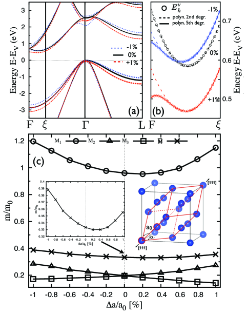
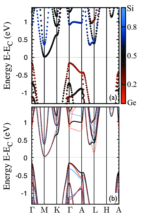
In figure 1(a) the uncorrected band structure of bulk silicon in the rhombohedral unit cell is shown for the unstrained case (black solid line), under tensile strain (red dashed line) and for compressive strain (blue dotted line) on relevant high symmetry lines. Unstrained silicon has an indirect band gap with conduction band minima (CBM) near the high symmetry point. The CBM consists of sixfold degenerate () prolate spheroidal isoenergetic surfaces along six equivalent directions. Due to symmetry of the lattice distortion in [111]-direction this degeneracy holds under applied strain in contrast to strain applied along [001]-direction [18].
In the unstrained case, for each -valley the effective masses along the major and the minor axis are and , respectively. As can be seen from figure 1(b) the idea of an effective mass determined by a second order polynomial fit (dashed lines in figure 1(b)) is valid for the unstrained case, but band warping leads to deviations for silicon under strain already for small band occupations. Here, a fifth order polynomial fit (solid lines in figure 1(b)) is necessary to reproduce the band dispersion, which occurs under applied biaxial [111]-strain. It is therefore advisable to go beyond a simplified effective mass model. Contrary to the conduction bands, the [111]-strain leads to a splitting of the degenerate valence bands, the heavy-hole (HH) and light-hole band (LH), similar to the case of [001]-strain [18, 42]. While the spin-orbit-split-off band is 40 meV away from the band edge, the HH band lifts up energetically under tensile strain, while the LH band lowers in energy. This picture reverses under opposite strain conditions [43]. While the indirect gap closes linearly under tensile in-plane strain from in equilibrium to about at , the gap size is almost constant within under compressive strain within the considered range [26, 44, 45] (comp. figure 1(b)). The direct gap at decreases slightly under applied strain, more pronounced under compressive in-plane strain.
The influence of biaxial in-plane strain on the fitted effective masses is summarized in figure 1(c). The change of the effective mass M1 along the major axis is almost symmetric to the applied strain and increases up to of the unstrained value. In contrast, the transverse effective masses behave drastically different. While the transverse effective mass M2 increases under tensile strain, the effective mass M3 perpendicular to M2 decreases. This behaviour is reversed under applied compressive strain. These results are in good agreement to other findings [44, 45], but add up to GW calculations were only one transverse mass with an almost constant value was found [26]. The strain-dependent averaged effective mass , often referred to as density-of-states effective mass, is shown additionally as an inset in figure 1(c).
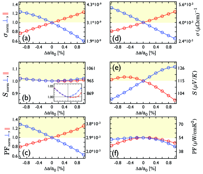
In the following the influence of trigonal distortion on the thermoelectric transport of Si under electron doping will be discussed. For this purpose two doping and temperature regimes are considered. The first, at a low temperature of and low charge carrier concentration of , is suitable for metal-oxide-semiconductor device applications. The results for the electrical conductivity, thermopower and power factor in dependence on the in-plane strain are shown in figure 2(a),(b) and (c), respectively. Under tensile strain the in-plane electrical conductivity increases almost linearly, while the cross-plane component decreases almost comparable. For compressive strain the behaviour reverses, with the cross-plane conductivity being enhanced up to 23 % at 1% compressive strain, while the in-plane conductivity decreases to nearly 23% of the unstrained value under 1% tensile strain. In the limit of a degenerate semiconductor at low temperatures and small charge carrier concentrations this results can be completely understood within an effective mass calculation [22]. With noticeable variation of the electrical conductivity under applied strain, the thermopower is almost unaffected. At low temperatures only a small energy window near the band edges plays an important role for the determination of the thermopower. As the functional change of the coefficients is determined by parabolic bands and a strain-dependent shift of the chemical potential, a strong change in the thermopower can not be expected. However, a slight upward tendency for the thermopower under compressive and tensile strain can be stated. As , this can be directly linked to the strain-dependence of (cf. figure 1(c)). For tensile strain an anisotropy of the thermopower is apparent, which seems to be suppressed for compressive strain. This could be linked to stronger deviations from the isotropic effective mass for tensile strain as shown in figure 1(b).
The strain-dependence of the resulting power factor PF is shown in figure 2(c). Due to the weak impact of the thermopower, the behaviour of the power factor is dominated by the electrical conductivity dependence on the applied strain. At low temperatures and small charge carrier concentrations, such a behaviour has already been observed for biaxially strained silicon [18]. However, the additional power-output described by the power factor is enhanced by 30% under applied 1% compressive strain for and by 25% under applied 1% tensile strain for . We note, that this low temperature and small doping case is not feasible for thermoelectric power generation, but could give inside in parasitic effects which play a role in metal-oxide-semiconductor devices.
Usual conditions for silicon-based thermoelectric applications, such as high temperature of 900 K and large charge carrier concentrations are assumed in figures 2(d)-(f). At temperatures of 900 K the electronic band structure on a width around the position of the chemical potential has to be considered, which makes a simplified description of the electronic transport properties within a spherical band picture inaccurate. However, the dependence of the electrical conductivity (ref. figure 2(d)) on the applied [111]-strain is almost preserved, even if accidentally. This is in contrast to biaxial strain in [001]-direction, were the strain-dependence induced by reoccupation of bands was suppressed under higher temperatures and dopings [18, 35].
In figure 2(e) the anisotropic thermopower under trigonal distortion is shown. The cross-plane thermopower shows a monotonous increase from 85% to 110% of the unstrained thermopower value of varying from compressive to tensile strain. The in-plane component decreases to 85% of the unstrained thermopower value under 1% tensile strain. A very similar behaviour was found for the thermopower of biaxially strained silicon in [001]-direction [18]. The compensation effects of the enhanced thermopower and decreased electrical conductivity and vice versa, are well known for thermoelectrics under strain [18, 21, 46]. This scenario holds for [111]-strained silicon, too. In figure 2(f) the shown anisotropic power factor in in-plane and cross-plane direction is always smaller than the power factor of the undistorted system, while being at least stable under small values of compressive strain. We mention that the absolute values (cf right scales in Figs. 2(a) and (d)) of the electrical conductivity are increased remarkably compared to the low doping case as expected. Due to this, the absolute value of the power factor raises in its absolute value, but unfortunately does not show an enhancement due to mechanical strain in [111]-direction. Furthermore, compared to the low-doping/low-temperature regime (figure 2(c)) the power factor does not show noticeable anisotropy between in-plane and cross-plane components.
3.2 [111]-strained silicon: hole doping
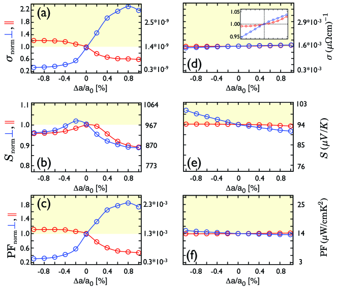
As it is well known, thermoelectric devices use two types of semiconductors, namely n-type and p-type, which are connected in series [6]. Therefore, the influence of biaxial [111]-strain on hole-doped silicon is presented in figure 3 in the same way as done for the electron-doped case. In the low-doping/low-temperature regime an enormous enhancement for the cross-plane electrical conductivity under sufficient tensile strain can be found (cf figure 3(a)), while the in-plane component decreases more slightly under the same strain conditions. This behaviour can be linked to a changed subband structure. As mentioned before, strain lifts the degeneracy of LH and HH bands around the point and alters the curvature, that is the effective mass, of both bands. Under applied strain, the valence bands become highly anisotropic and a crossover between bands occurs so that they even loose their original LH and HH meaning[18, 25]. Extended discussions here on can be found in refs. [43, 47].
The thermopower of p-type silicon is shown in figure 3(b). The thermopower in-plane and cross-plane decreases slightly under tensile, as well as under compressive strain. The anisotropy of the thermopower is moderate. As previously reported [18, 48], the thermopower depends strongly on the number of occupied carrier pockets. A higher valley degeneracy at a fixed charge carrier concentration leads to an increased thermopower. As already mentioned the formerly degenerate HH and LH bands split under tensile and compressive strain. At low hole concentrations and low temperatures only the former HH (LH) band is occupied. This leads directly to a reduction of and . Consequently, the accompanied power factor (cf. figure 3(c)) is also reduced in its maximal possible enhancement, but follows in principle the behaviour given by the electrical conductivity.
For high temperatures and high hole concentrations the results are shown in figures 3(d)-(f). As the carrier concentration is raised by nearly six orders of magnitude with respect to the low doping case, the absolute value of the electrical conductivity raises in the same order (note the right scale of figure 3(d)). Unfortunately, due to the higher band occupation and the broader smearing of the Fermi-Dirac- distribution, effects of redistribution in strain-split bands do not play a role any more. Moreover, the effects of reduced and increased effective masses cancel each other leading to negligible change, in absolute values as well as in anisotropy, of the hole electrical conductivity.
For the hole thermopower shown in figure 3(e) this behaviour is still valid. For the in-plane thermopower no significant influence of either compressive or tensile strained could be found. A minor dependence on applied [111]-strain is observed for . Here, the cross-plane thermopower decreases from to for strain values varying from 1% compressive to 1% tensile strain.
Comprising the results for the electrical conductivity and thermopower, the resulting power factor under hole doping is shown in figure 3(f). No evident influence of [111]-strain on the power factor could be found in the thermoelectrically relevant temperature and hole doping regime. Furthermore, the absolute value of the power factor is about 3-4 times smaller than in the comparable electron doped case, which is mainly caused by the higher hole scattering rate as assumed in Eq. 3.
At varying strain not only the absolute values of the thermoelectric properties change, but also the optimal charge carrier concentrations to obtain these maximized values. For biaxially [001]-strained silicon it was found, that the optimal doping range can change by a factor of two, while reducing the power factor up to 20% if not adapting the charge carrier concentration [18]. Therefore, the in-plane and cross-plane power factor under varying electron- and hole-doping, as well as varying [111]-strain is shown in figure 4. The maximized power factor at optimal charge carrier concentration at a given strain state is emphasized by a black-dotted line in figures 4(a)-(d). Comparing silicon under electron doping (cf figures 4(a),(b)) and hole doping (cf. figure 4(c),(d)), it is obvious, that electron-doped silicon shows a much stronger variation of the optimal doping range. For the in-plane component and electron-doping the optimal carrier concentration decreases by about a factor 5, from to with the strain changing from 1% compressive to 1% tensile strain. For the corresponding cross-plane power factor the optimal carrier concentration is about at 1% compressive strain and increases by about a factor 5 under same strain conditions. At hole-doping no evident change of the optimal doping could be found at varying strain, while the absolute value depends only weakly on the applied strain (cf. figure 3(f)).
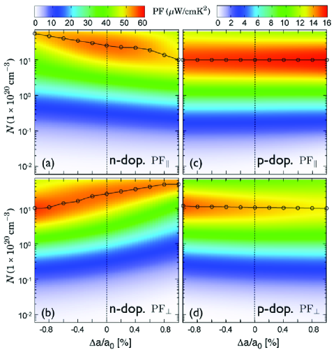
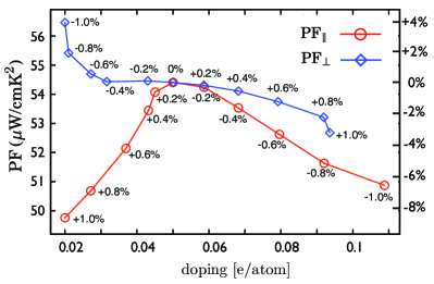
To summarize our findings, sections along the path of optimal electron doping are shown in figure 5. With this, it is obvious that even with optimized doping no enhancement by tensile or compressive [111]-strain can be obtained for the in-plane power factor . For the cross-plane component , which is more relevant for possible SL’s, an increase of the power factor of about 4% at 1% compressive strain was found. To obtain this rather small enhancement the electron charge carrier concentration has to be reduced by about a factor of 2.5 compared to the unstrained case.
3.3 Strained Si/Ge-SL on Si[111]
By introducing the concepts of carrier pocket engineering [15, 16, 17] and phonon-glass/electron-crystal [49, 50] to semiconducting SLs an enormous leap forward to maximize the thermoelectric FOM was proposed. Indeed, several proofs-of-principle showed a remarkable enhancement of the FOM for thermoelectric semiconducting heterostructures [7, 8, 17, 51]. With the thermal conductivity of SL’s far below their alloy limit [52, 53, 54, 55] and their constituents bulk values, a main task in optimizing the FOM is to enhance or at least to retain advantageous electronic properties of the bulk materials, so to say the power factor. For silicon-based SL’s, carrier pocket engineering can be triggered by lattice strain. Using Si1-x/Gex substrates in [111] and [100] orientation a and , respectively, were predicted for strain-symmetrized222For an introduction to strain-symmetrized and strain-non-symmetrized Si/Ge superlattices we refer to the publications of Kasper et al.[56, 57]. Si(20Å)Ge(20Å) SL’s at room temperature. The latter case was experimentally confirmed with at [17], which is nevertheless about a sevenfold enhancement relative to bulk Si [13, 18]. These experimental findings encourage further research for strain-non-symmetrized Si(20Å)/Ge(20Å) SLs in [001]-orientation and Si(15Å)/Ge(40Å) SLs in [111]-orientation, with and , respectively, predicted at [15].
While being in principle possible for very thin films [58, 59], to our best knowledge state-of-the-art thin film technology does not enable strain-non-symmetrized SL’s with satisfactory structural qualities and thicknesses for thermoelectric applications so far [56, 57, 60, 61]. Nevertheless, in the following the thermoelectric transport properties of a strain-non-symmetrized Si(5Å)/Ge(5Å) SL in [111]-orientation will be discussed, as the largest enhancement of the FOM is expected here[15].
The used Si(5Å)/Ge(5Å) SL is represented by a hexagonal six-atom unit cell (ref. inset in figure 7(a)) with point group symmetry and a fixed in-plane lattice constant of Å was used to simulate the bulk silicon substrate. Structural optimization of the atomic positions and the c-axis elongation of the unit cell were obtained using VASP [27]. The distinct interlayer distances in [111]-direction were determined as Å, Å, Å , Å, Å, Å and are in good agreement with previous calculations [62]. The ratio shows an increase of the lattice constant in c-direction by about 4% compared to bulk Si. This is clearly dictated by the fixed in-plane Si lattice constant and the larger volume of Ge. Due to this, the Ge layer can be seen as compressively strained in [111]-direction.
As has already been mentioned in literature [62, 63], the face centred cubic (fcc) L high symmetry point in the [111] direction folds onto the hexagonal A high symmetry point at a -ratio of . In addition, the fcc X point is equivalent to the hexagonal M point, while the symmetry directions fcc X and hexagonal M are inequivalent. This is due the fcc X point lying in an adjoining Brillouin zone. Under biaxial [111]-strain two inequivalent sets of the eight L points occur. There are two points along c-axis in [111] direction of growth which fold onto the A point and those in the six directions equivalent to [] hereafter noted as L.
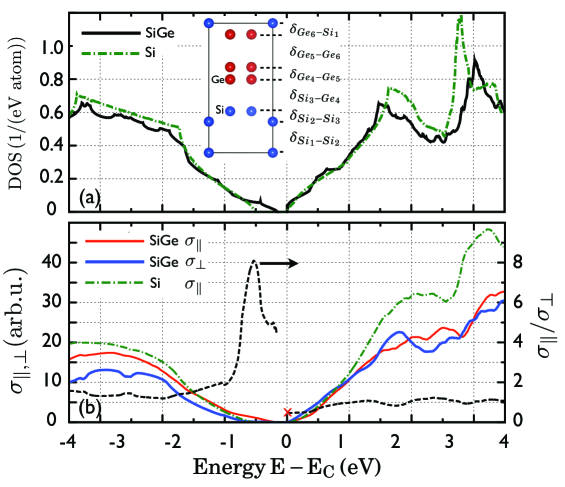
In figure 6 the band structure for the fully relaxed Si/Ge-SL in the hexagonal unit-cell is shown. While in figure 6(a) the site-resolved bands for the Si/Ge-SL are depicted, in figure 6(b) the bands for pure Si on the fully-relaxed Si/Ge-positions are shown (blue, dashed lines), as well as all sites occupied by Ge (red, dotted lines) and the bands referring to the original Si/Ge-SL bands as shown in figure 6(a) (black, solid lines). Two main insights can be drawn. First, the VBM is located around the point and has an almost pure Ge character, given by the red dots in figure 6(a). This is mainly due to the smaller band gap of Ge and the accompanied band offset between Ge and Si. Furthermore, the compressive biaxial strain in the Ge layers decreases the gap size and favours a direct band gap at instead of an indirect one between and L [64, 45, 65]. Valence bands of mixed Si/Ge character come in to play around below CBM and suggest the local indirect Si band gap between and M to be almost retained bulk like. Second, the CBM is located at the M point and shows a strong mixing of Si and Ge character. Furthermore a strain-induced lifting of degeneracy occurs at the M point lowering a band of mixed character to the band edge and lifting a Si-like band upwards in energy. As only the Ge layers in the SL are compressively strained while the Si layers are nearly unstrained, the Ge L-point CBM valleys split into valleys located at A higher in energy and in L valleys lower in energy [15, 65, 66]. These findings on the CBM and VBM characteristics are in agreement to experimental studies [59]. With that the uncorrected band gap decreases to around , which is about 30% of the uncorrected GGA gap for unstrained bulk Si. Furthermore, the effective masses at the CBM lower to M1=, M2= and M3= 333The referring Eigenvectors were determined as , and .. Applying an effective mass approach [22] we find the conductivity anisotropy for energies near the CBM to =0.6, which clearly prefers cross-plane transport under electron-doping.
The energy-dependent transport distribution function in the in-plane and cross-plane direction and their ratio are displayed in figure 7(b) for the Si/Ge-SL and isotropic unstrained bulk Si. For the same systems the density of states are shown in figure 7(a). As can be seen from figure 7(b) unfortunately the conductivity anisotropy near the valence band edge strongly increases to values of 8 around below CBM, clearly suppressing cross-plane electronic transport under p-type doping. This behaviour is largely due to the localization of the Ge like VBM states, in space as well as energy. As can be deduced from figure 6(a) bands in the cross-plane direction (here A) show pure Ge band character in an energy range of below CBM. Clearly, in this energy range cross-plane conduction is suppressed by states localized in the Ge layers and almost vanishing in the Si layers leading to a strongly increased conductivity anisotropy. At an energy of below CBM at a light band with strong Si/Ge mixed character appears (cf. black solid line in figure 6(b)) leading to cross-plane transport through the Si and Ge layer forcing to decrease, while saturating for values above 1, still indicating a preferred in-plane transport under hole-doping.
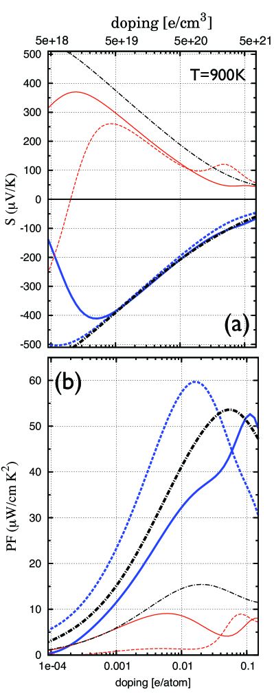
In figure 8(a),(b) the doping-dependent thermopower and power factor for the Si/Ge-SL are shown, respectively. As a comparison the reference values of bulk silicon are stated as black, dashed-dotted lines. We note, that a temperature dependency of the energy gap was introduced applying Eq. 2. For the Si/Ge-SL 444Here we adapted experimental data for Si0.5Ge0.5 alloys from Ref. [67]. the parameters are chosen as and . However, in the highly degenerate limit () the temperature dependence of the gap plays a negligible role even for temperatures above .
From figure 8(a) it can be seen, that the thermopower in the Si/Ge-SL under electron doping (blue lines in the lower panel) is comparable to bulk silicon and follows a Pisarenko relation [68]. Under hole doping (red lines in the upper panel) the thermopower is suppressed compared to bulk silicon by about for and in the relevant doping regime, which might be linked to a changed functional behaviour of the TDF . The latter can be deduced from figure 7(b) where apparent differences in the functional behaviour of , which is proportional to , are visible especially in the valence bands of bulk Si and the Si/Ge-SL. The clear deviation of from the Pisarenko relation in the vicinity of is related to the strongly increased conductivity anisotropy below VBM as shown in figure 7(b). Here, the strong suppression of causes a larger . Nevertheless, this slight enhancement of is not reflected in the power factor of the p-type Si/Ge-SL. As shown in figure 8(b) , as well as are always smaller than the values for bulk Si under hole doping (red lines). Obviously, the suppressed electrical conductivity, especially in the cross-plane direction, is responsible for this result. A power factor of about is found for at , while in the cross-plane direction the same value can be stated at huge values of , clearly evoked by the anomaly in the thermopower. More interesting is the case of electron doping (blue lines in figure 8(a)). With the thermopower’s behaviour almost bulk like and conductivity anisotropies below 1 an enhanced power factor in the required cross-plane direction is found. Compared to bulk silicon the is enhanced by 10% and reaches a value of at an electron concentration of . With that the optimal charge carrier concentration is four-times smaller compared to bulk Si. For the in-plane component almost no reduction can be seen, while the maximal value of is shifted to slightly larger charge carrier concentrations.
3.4 Towards the figure of merit
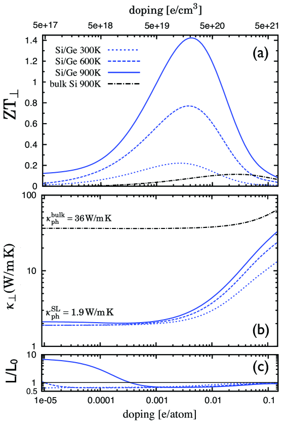
In figure 9(a) the FOM in cross-plane direction for the Si/Ge-SL (blue lines) and the more promising electron-doped case is shown. Different temperatures are chosen to demonstrate the evaluation of maximal ZT and the range of optimal charge carrier concentration. As a comparison the FOM for bulk Si is shown as black dashed-dotted line, too. To present results for the FOM, knowledge of the thermal conductivity is relevant. For this purpose, the electronic part of the thermal conductivity was calculated applying Eq. 6, while the lattice part was taken from experiment. Here, [13] was used for bulk Si at , while was used for the Si/Ge-SL [55]. With the latter being rather optimistic, since smaller than the expected nano-alloy limit of [69], but achievable in Si/Ge-SL [53, 55, 70]. However, from figure 9(b) one can deduce that for thermoelectric reliable charge carrier concentrations above the electronic contribution to the total thermal conductivity dominates over its lattice part. At for the electronic part amounts to clearly smaller than the lattice part. This contribution increases significantly at higher temperatures and charge carrier concentrations omitting higher absolute values of the FOM. However, ZT⟂ above unity can be reached for operating temperatures higher than and electron-doping .
At room-temperature a ZT is achieved in a broad doping range of . Besides this value being an order of magnitude higher than the bulk Si value of ZT [13, 15, 18], it is still less than the postulated values of ZT and ZT by Koga et al.[15] for strain-symmetrized and strain-non-symmetrized Si/Ge-SL, respectively. With that, and using a rather conservative value of for their estimations, they expect enormous power factors of PF and PF for the strain-optimized Si/Ge-SL in [111]-direction. We found PF at and for the Si/Ge-SL. Even though a convergence of carrier pockets is not fully achieved in our superlattice, power factors beyond seem to be very sophisticated, as state-of-the art power factors near or above room-temperature are well below [7, 71, 72]. A benefit from thermoionic emission even at moderate temperatures can not be expected in Si/Ge-SL [73, 74, 75]. We note, that at very low temperatures below huge PF of about were reported for bulk Fe2Sb2 and ZnO1-xSex [76, 77].
As an addition in figure 9(c) the doping-dependent Lorenz function as defined via equations (5) and (6) is presented. From figure 9(c) it is obvious that the Lorenz number can be substantially different from the metallic limit . Nevertheless, for very large charge carrier concentrations and the chemical potential located deep inside the conduction band, almost coincides with . At intermediate and thermoelectric relevant charge carrier concentrations of can be much smaller than . For and we find a minimal value of . At smaller charge carrier concentrations rapidly increases and reaches for electron charge carrier concentrations of in the intrinsic doping regime. At decreasing temperatures minimal values of the Lorenz function are obtained at much smaller charge carrier concentrations. Furthermore, the maximal values of shifts to smaller charge carrier concentrations, too, and can reach huge values of at very low temperatures and charge carrier concentrations. The effect, which is responsible for the suppression of the Lorenz function to values below the metallic limit is termed bipolar thermodiffusion effect [78, 79, 80] and maximizes for positions of the chemical potential near the band edges. However, a Lorenz function can have consequences for the determination of the thermal conductivity. The Lorenz factor is generally used to separate and . At thermoelectric advisable charge carrier concentrations applying the metallic value to determine the lattice thermal conductivity could lead to an overestimation of the electronic thermal conductivity, and consequently to an underestimation of the lattice contribution.
4 Conclusions and Outlook
With the presented results we have shown, that strain in [111]-direction is not sufficient to significantly enhance the thermoelectric transport properties in bulk Si for energy harvesting applications. In the low-temperature and low-doping case large enhancements were found at tensile strain for (electron-doping) and (hole-doping) and under compressive strain for (electron-doping). This could have a negative impact for metal-oxide-semiconductor devices involving [111]-strained Si. Here, in the low-temperature and low-doping regime, small temperature gradients in the devices could lead to an additional parasitic electrical power, which can be way larger than expected from unstrained bulk.
Enhancements found in the high-temperature and high doping regime were distinct smaller. Here slight enhancements of 5% for were found under compressive strain. The more interesting is, that the power factor is robust against [111]-strain, especially under hole-doping. Thus, thermoelectric SLs based on [111]-strained Si could provide an enhanced FOM, as is most likely reduced in SLs. We note, that due the to high bulk thermal conductivity and the only modest gain in the power factor by [111]-strain engineering, bulk silicon remains an unfavourable thermoelectric, even if the electronic transport properties are strain optimized. However, from comparison with earlier studies on biaxially [001]-strained silicon [18], we confirm that strain in [111]-direction, e.g. in silicon-based SLs, should be preferred, as the carrier pocket degeneracy is retained and therefore the thermopower and power factor can be maximized.
To deal with that, we investigated the anisotropic thermoelectric transport of an [111]-oriented Si/Ge superlattice. At a first glance we have shown that no degradation of the electronic transport by the heterostructure is expected for electron doping, while even showing an enhancement of 10% in compared to bulk Si. Assuming a decrease in lattice thermal conductivity a large enhancement in ZT to 0.2 and 1.4 is achieved at and , respectively. Under hole doping the electronic transport in the Si/Ge-SL is heavily suppressed due to quantum well effects. Here the cross-plane power factor is expected to show only around 50% of the bulk maximal value, leading to small ZT values.
References
References
- [1] T. J. Seebeck. Über die magnetische Polarisation der Metalle und Erze durch Temperatur-Differenz. Annalen der Physik, 82:253–286, 1826.
- [2] A. F. Ioffe. The revival of thermoelectricity. Scientific American, 199:31–37, 1958.
- [3] A Majumdar. Thermoelectricity in Semiconductor Nanostructures. Science, 303(5659):777, 2004.
- [4] H Böttner, G Chen, and R Venkatasubramanian. Aspects of Thin-Film Superlattice Thermoelectric Materials, Devices, and Applications. MRS bulletin, 31:211, 2006.
- [5] T.M Tritt and MA Subramanian. Thermoelectric materials, phenomena, and applications: A bird’s eye view. MRS bulletin, 31(03):188–198, 2006.
- [6] BC Sales. Thermoelectric materials: Smaller is cooler. Science, 295(5558):1248, 2002.
- [7] R Venkatasubramanian, E Siivola, and T Colpitts. Thin-film thermoelectric devices with high room-temperature figures of merit. Nature, 413:597, 2001.
- [8] T Harman, P Taylor, M Walsh, and B LaForge. Quantum dot superlattice thermoelectric materials and devices. Science, 297:2229, 2002.
- [9] M Dresselhaus, G Chen, M Tang, and R Yang. New directions for low-dimensional thermoelectric materials. Advanced Materials, 19:1, 2007.
- [10] CB Vining. Materials science: Desperately seeking silicon. Nature, 451(7175):132–133, 2008.
- [11] A Hochbaum, R Chen, R Delgado, and W Liang. Enhanced thermoelectric performance of rough silicon nanowires. Nature, 451:163, 2008.
- [12] AI Boukai, Y Bunimovich, J Tahir-Kheli, JK Yu, WA Goddard Iii, and JR Heath. Silicon nanowires as efficient thermoelectric materials. Nature, 451(7175):168–171, 2008.
- [13] Sabah K Bux, Richard G Blair, Pawan K Gogna, Hohyun Lee, Gang Chen, Mildred S Dresselhaus, Richard B Kaner, and Jean-Pierre Fleurial. Nanostructured Bulk Silicon as an Effective Thermoelectric Material. Adv. Funct. Mater., 19(15):2445–2452, 2009.
- [14] J Tang, H.T Wang, D.H Lee, M Fardy, Z Huo, T.P Russell, and P Yang. Holey Silicon as an Efficient Thermoelectric Material. Nano Lett, 10:4279, 2010.
- [15] T Koga, X Sun, SB Cronin, and MS Dresselhaus. Carrier pocket engineering applied to strained si/ge superlattices to design useful thermoelectric materials. Applied Physics Letters, 75:2438, 1999.
- [16] T Koga, T Harman, S Cronin, and M Dresselhaus. Mechanism of the enhanced thermoelectric power in (111)-oriented n-type PbTe/Pb1-xEuxTe multiple quantum wells. Phys. Rev. B, 60(20):14286, 1999.
- [17] T Koga, S Cronin, M Dresselhaus, and J Liu. Experimental proof-of-principle investigation of enhanced ZT in (001) oriented Si/Ge superlattices. Applied Physics Letters, 77(10), 2000.
- [18] N Hinsche, I Mertig, and P Zahn. Effect of strain on the thermoelectric properties of silicon: an ab initio study. J. Phys.: Condens. Matter, 23:295502, 2011.
- [19] Paolo Giannozzi, Stefano Baroni, Nicola Bonini, Matteo Calandra, Roberto Car, Carlo Cavazzoni, Davide Ceresoli, Guido Chiarotti, Matteo Cococcioni, Ismaila Dabo, Andrea Dal Corso, Stefano De Gironcoli, Stefano Fabris, Guido Fratesi, Ralph Gebauer, Uwe Gerstmann, Christos Gougoussis, Anton Kokalj, Michele Lazzeri, Layla Martin-Samos, Nicola Marzari, Francesco Mauri, Riccardo Mazzarello, Stefano Paolini, Alfredo Pasquarello, Lorenzo Paulatto, Carlo Sbraccia, Sandro Scandolo, Gabriele Sclauzero, Ari Seitsonen, Alexander Smogunov, Paolo Umari, and Renata Wentzcovitch. Quantum espresso: a modular and open-source software project for quantum simulations of materials. J. Phys.: Condens. Matter, 21:395502, 2009.
- [20] I Mertig. Transport properties of dilute alloys. Reports on Progress in Physics, 62:237–276, 1999.
- [21] N Hinsche, B Yavorsky, I Mertig, and P Zahn. Influence of strain on anisotropic thermoelectric transport in Bi2Te3 and Sb2Te3. Physical Review B, 84(16):165214, 2011.
- [22] Peter Zahn, Nicki Hinsche, B Yavorsky, and Ingrid Mertig. Bi2Te3: implications of the rhombohedral k-space texture on the evaluation of the in-plane/out-of-plane conductivity anisotropy. J. Phys.: Condens. Matter, 23:505504, 2011.
- [23] JP Perdew, K Burke, and M Ernzerhof. Generalized gradient approximation made simple. Phys. Rev. Lett., 77(18):3865–3868, 1996.
- [24] A Corso and A Conte. Spin-orbit coupling with ultrasoft pseudopotentials: Application to au and pt. Phys. Rev. B, 71:115106, 2005.
- [25] D Yu, Y Zhang, and F Liu. First-principles study of electronic properties of biaxially strained silicon: Effects on charge carrier mobility. Physical Review B, 78(24):245204, 2008.
- [26] M Bouhassoune and A Schindlmayr. Electronic structure and effective masses in strained silicon. physica status solidi (c), 7(2):460–463, 2009.
- [27] G Kresse and J Furthmüller. Efficient iterative schemes for ab initio total-energy calculations using a plane-wave basis set. Physical Review B, 54(16):11169, 1996.
- [28] RW Godby, M Schlüter, and LJ Sham. Self-energy operators and exchange-correlation potentials in semiconductors. Physical Review B, 37(17):10159–10175, 1988.
- [29] YP Varshni. Temperature dependence of the energy gap in semiconductors. Physica, 34(1):149–154, 1967.
- [30] T Vojta, I Mertig, and R Zeller. Calculation of the residual resistivity and the thermoelectric power of sp impurities in silver. Phys. Rev. B, 46(24):16761, 1992.
- [31] T Thonhauser, TJ Scheidemantel, and JO Sofo. Improved thermoelectric devices using bismuth alloys. Applied Physics Letters, 85:588, 2004.
- [32] David J Singh. Doping-dependent thermopower of PbTe from Boltzmann transport calculations. Physical Review B, 81(19):195217, 2010.
- [33] TJ Scheidemantel, C Ambrosch-Draxl, T Thonhauser, JV Badding, and JO Sofo. Transport coefficients from first-principles calculations. Physical Review B, 68(12):125210, 2003.
- [34] C Jacoboni, C Canali, G Ottaviani, and A Alberigi Quaranta. A review of some charge transport properties of silicon. Solid-State Electronics, 20(2):77–89, 1977.
- [35] T Dziekan, P Zahn, V Meded, and S Mirbt. Theoretical calculations of mobility enhancement in strained silicon. Physical Review B, 75(19):195213, 2007.
- [36] J B Roldán, F Gámiz, J A López‐Villanueva, and J E Carceller. A Monte Carlo study on the electron‐transport properties of high‐performance strained‐Si on relaxed SiGe channel MOSFETs. Journal of Applied Physics, 80(9):5121, 1996.
- [37] G Mahan and JO Sofo. The best thermoelectric. Proceedings of the National Academy of Sciences, 93:7436, 1996.
- [38] G Lehmann and M Taut. On the Numerical Calculation of the Density of States and Related Properties. physica status solidi (b), 54(2):469–477, 1972.
- [39] P Zahn, I Mertig, M Richter, and H Eschrig. Ab Initio Calculations of the Giant Magnetoresistance. Phys. Rev. Lett., 75(16):2996–2999, 1995.
- [40] Ingrid Mertig, Eberhard Mrosan, and Paul Ziesche. Multiple scattering theory of point defects in metals: Electronic properties. B.G. Teubner, Leipzig, 1987.
- [41] Koichi Momma and Fujio Izumi. VESTA3 for three-dimensional visualization of crystal, volumetric and morphology data. Journal of Applied Crystallography, 44(6):1272–1276, Dec 2011.
- [42] Mehmet O Baykan, Scott E Thompson, and Toshikazu Nishida. Strain effects on three-dimensional, two-dimensional, and one-dimensional silicon logic devices: Predicting the future of strained silicon. Journal of Applied Physics, 108(9):093716, 2010.
- [43] Guangyu Sun, Yongke Sun, Toshikazu Nishida, and Scott E Thompson. Hole mobility in silicon inversion layers: Stress and surface orientation. Journal of Applied Physics, 102(8):084501, 2007.
- [44] Timothy Boykin, Neerav Kharche, and Gerhard Klimeck. Brillouin-zone unfolding of perfect supercells having nonequivalent primitive cells illustrated with a Si∕Ge tight-binding parameterization. Phys. Rev. B, 76(3):035310, 2007.
- [45] Y Niquet, D Rideau, C Tavernier, H Jaouen, and X Blase. Onsite matrix elements of the tight-binding hamiltonian of a strained crystal: Application to silicon, germanium, and their alloys. Physical Review B, 79(24):245201, 2009.
- [46] Min Sik Park, Jung-Hwan Song, Julia E Medvedeva, Miyoung Kim, In Gee Kim, and Arthur J Freeman. Electronic structure and volume effect on thermoelectric transport in p -type bi and sb tellurides. Phys. Rev. B, 81(15):155211, 2010.
- [47] S.E Thompson, G Sun, Y.S Choi, and T Nishida. Uniaxial-process-induced strained-Si: extending the CMOS roadmap. IEEE Transactions on Electron Devices, 53(5):1010–1020, 2006.
- [48] Yanzhong Pei, Xiaoya Shi, Aaron LaLonde, Heng Wang, Lidong Chen, and G. Jeffrey Snyder. Convergence of electronic bands for high performance bulk thermoelectrics. Nature, 473(7345):66–69, 2011.
- [49] Glen A. Slack. CRC Handbook of Thermoelectrics, chapter 34, page 407. CRC Press, Boca Raton, 1995.
- [50] B Poudel, Q Hao, Y Ma, Y Lan, A Minnich, B Yu, X Yan, D Wang, A Muto, and D Vashaee. High-thermoelectric performance of nanostructured bismuth antimony telluride bulk alloys. Science, 320(5876):634, 2008.
- [51] L Hicks, T Harman, X Sun, and M Dresselhaus. Experimental study of the effect of quantum-well structures on the thermoelectric figure of merit. Physical Review B, 53(16):R10493–R10496, 1996.
- [52] R Venkatasubramanian. Lattice thermal conductivity reduction and phonon localizationlike behavior in superlattice structures. Phys. Rev. B, 61(4):3091–3097, 2000.
- [53] T Borca-Tasciuc. Thermal conductivity of symmetrically strained Si/Ge superlattices. Superlattices and Microstructures, 28(3):199–206, 2000.
- [54] S Chakraborty, CA Kleint, A Heinrich, CM Schneider, J Schumann, M Falke, and S Teichert. Thermal conductivity in strain symmetrized Si/Ge superlattices on Si (111). Applied Physics Letters, 83:4184, 2003.
- [55] S Lee, D Cahill, and R Venkatasubramanian. Thermal conductivity of Si–Ge superlattices. Appl. Phys. Lett., 70:2957, 1997.
- [56] E Kasper, H Kibbel, H Jorke, H Brugger, E Friess, and G Abstreiter. Symmetrically strained Si/Ge superlattices on Si substrates. Physical Review B, 38(5):3599–3601, Aug 1988.
- [57] E Kasper. Growth and properties of Si/SiGe superlattices. Surface Science, 174(1-3):630–639, Jan 1986.
- [58] T Pearsall, J Bevk, L Feldman, J Bonar, J Mannaerts, and A Ourmazd. Structurally induced optical transitions in Ge-Si superlattices. Phys. Rev. Lett., 58(7):729–732, Feb 1987.
- [59] T Pearsall, J Bevk, J Bean, J Bonar, J Mannaerts, and A Ourmazd. Electronic structure of Ge/Si monolayer strained-layer superlattices. Physical Review B, 39(6):3741–3757, Feb 1989.
- [60] K Brunner. Si/Ge nanostructures. Reports on Progress in Physics, 65:27, 2002.
- [61] T. S. Kuan and S. S. Iyer. Strain relaxation and ordering in SiGe layers grown on (100), (111), and (110) Si surfaces by molecular-beam epitaxy. Appl. Phys. Lett., 59:2242, 1991.
- [62] JM Bass and CC Matthai. Electronic structure of (111) Si/Ge superlattices. J. Phys.: Condens. Matter, 2:7841, 1990.
- [63] MR Salehpour and S Satpathy. Comparison of electron bands of hexagonal and cubic diamond. Physical Review B, 41(5):3048, 1990.
- [64] H Tahini, A Chroneos, R W Grimes, U Schwingenschlögl, and A Dimoulas. Strain-induced changes to the electronic structure of germanium. J. Phys.: Condens. Matter, 24(19):195802.
- [65] Feng Zhang, Vincent Crespi, and Peihong Zhang. Prediction that Uniaxial Tension along ⟨111⟩ Produces a Direct Band Gap in Germanium. Phys. Rev. Lett., 102(15):156401, 2009.
- [66] D Rideau, M Feraille, L Ciampolini, M Minondo, C Tavernier, H Jaouen, and A Ghetti. Strained Si, Ge, and Si1−xGex alloys modeled with a first-principles-optimized full-zone k∙p method. Physical Review B, 74(19):195208, 2006.
- [67] Rubin Braunstein, Arnold R. Moore, and Frank Herman. Intrinsic optical absorption in germanium-silicon alloys. Phys. Rev., 109:695–710, 1958.
- [68] A. F. Ioffe. Physics of Semiconductors. Academic, New York, 1960.
- [69] XW Wang, H Lee, YC Lan, GH Zhu, G Joshi, DZ Wang, J Yang, AJ Muto, MY Tang, and J Klatsky. Enhanced thermoelectric figure of merit in nanostructured n-type silicon germanium bulk alloy. Applied Physics Letters, 93:193121, 2008.
- [70] G Pernot, M Stoffel, I Savic, F Pezzoli, P Chen, G Savelli, A Jacquot, J Schumann, U Denker, and I Mönch. Precise control of thermal conductivity at the nanoscale through individual phonon-scattering barriers. Nature Materials, 9:491, 2010.
- [71] B Jalan and Susanne Stemmer. Large Seebeck coefficients and thermoelectric power factor of La-doped SrTiO3 thin films. Applied Physics Letters, 97(4):3, 2010.
- [72] Noriyuki Okinaka and Tomohiro Akiyama. Latent Property of Defect-Controlled Metal Oxide: Nonstoichiometric Titanium Oxides as Prospective Material for High-Temperature Thermoelectric Conversion. Japanese Journal of Applied Physics, 45(9):7009–7010, 2006.
- [73] Daryoosh Vashaee and Ali Shakouri. Thermionic power generation at high temperatures using SiGe/Si superlattices. Journal of Applied Physics, 101(5):053719, 2007.
- [74] A Shakouri and J.E Bowers. Heterostructure integrated thermionic coolers. Applied Physics Letters, 71:1234, 1997.
- [75] D Vashaee and A Shakouri. Improved thermoelectric power factor in metal-based superlattices. Phys. Rev. Lett., 92(10):106103, 2004.
- [76] Peijie Sun, Niels Oeschler, Simon Johnsen, Bo B Iversen, and Frank Steglich. Huge Thermoelectric Power Factor: FeSb2 versus FeAs2 and RuSb2. Applied Physics Express, 2(9):091102, 2009.
- [77] Joo-Hyoung Lee, Junqiao Wu, and Jeffrey C Grossman. Enhancing the Thermoelectric Power Factor with Highly Mismatched Isoelectronic Doping. Phys. Rev. Lett., 104(1):016602, 2010.
- [78] G. S. Nolas and H. J. Goldsmid. Thermal conductivity: theory, properties, and applications, chapter 1.4, page 110. Kluwer Academic, New York, 2004.
- [79] L Chaput, P Pécheur, J Tobola, and H Scherrer. Transport in doped skutterudites: Ab initio electronic structure calculations. Phys. Rev. B, 72, 2005.
- [80] E Flage-Larsen and O Prytz. The lorenz function: Its properties at optimum thermoelectric figure-of-merit. Applied Physics Letters, 99(20):202108, 2011.