Shot noise suppression in InGaAs/InGaAsP quantum channels
Abstract
We have measured the shot noise in a quantum point contact (QPC) fabricated by using InGaAs/ InGaAsP heterostructure, whose conductance can be electrically tuned by the gate voltages. The reduced shot noise is observed when the QPC conductance equals to , which is the direct experimental evidence of the coherent quantized channel formation in the QPC. The deviation of the observed Fano factor from the theory is explained by the electron heating effect generated at the QPC.
InGaAs-based devices are attracting great interest these days since the InGaAs two-dimensional heterostructure possesses a strong spin-orbit interaction (SOI), which provides us ample opportunities to perform electrical spin generation MurakamiScience2003 ; KatoScience2004 , manipulation DattaAPL1989 ; KogaPRB2006 , and detection OhePRB2005 in solid state devices. Among various InGaAs-based systems including selfassembled quantum dots and nano whiskers Nadj-PergeNature2010 , the twodimensional electron gas (2DEG) system is an ideal stage to address spin-dependent coherent quantum transport KogaPRB2006 ; NittaPRL1997 ; KogaPRL2002 . Indeed, in 1980 s and 1990 s, mesoscopic systems represented by Aharonov-Bohm (AB) rings and the quantum point contacts (QPCs) WeesPRL1988 ; WharamJPC1988 on GaAs-based 2DEG have served to establish quantum transport DattaCUP1995 . In the same way but in focusing more on the role of spins, the AB rings on InGaAs 2DEG were studied to demonstrate the electron spin interference a few years ago BergstenPRL2006 . Spin resolved quantized conductance in the InAs QPC was reported very recently DebrayNatNano2009 . Thus, the quantum spin transport in the mesoscopic systems made of InGaAs 2DEG is now being started to be exploered KohdaPRB2010 ; EngelsPRB1997 , although there remains much to be addressed when compared to what have been done for those in GaAs-based 2DEG.
Shot noise is a powerful tool to study quantum transport in mesoscopic systems BlanterPR2000 . For example, the shot noise measurement was performed for the QPC on GaAs 2DEG already in 1990 (Ref. DekkerPRL1991 ) followed by the works by Reznikov et al. ReznikovPRL1995 and Kumar et al. KumarPRL1996 , who showed that the Fano factor is suppressed at the conductance plateau. This shot noise suppression, which is essentially originated from the Pauli principle of electrons, is a significant consequence of the formation of the coherent quantized channels. Moreover, the shot noise is expected to be useful to investigate coherent spin transport and spin correlation FevePRB2002 ; EguesPRL2002 . However, no report on the shot noise has been available for the InGaAs-based QPCs MartinPRB2008 ; SchapersAPL2007 ; SimmondsAPL2008 .
Here, we report the shot noise study of the QPC made by using InGaAs/InGaAsP 2DEG, where strong SOI exists.KohdaPRB2010 We found that the shot noise is reduced at the conductance plateaus of . This is the direct experimental evidence of the coherent quantized channels in the InGaAs-based QPC. We also discuss the heating effect to explain the deviation of the observed Fano factor from the conventional shot noise theory. The present shot noise study is a step forward to further explore quantum spin transport in InGaAs-based systems.
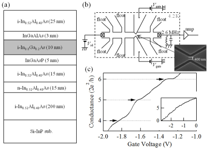
Figure 1(a) shows the heterostructure consisting of the following layers on an InP substrate: , , , i-InGaAsP , , InGaAlAs , and . 2DEG formed in layer has the carrier density of with the electron mobility of at . Our QPC structure was fabricated from this heterostructure defined by in-plane side gates patterned using the electron beam lithography and the reactive ion etching. The conductance and noise measurements were performed on the QPC with a gate voltage applied at liquid helium temperature (Fig.1(b)). Figure 1(c) shows the conductance of the QPC as a function of . While the relevance of the spin-dependent transport was observed in this system for the low conductance region below KohdaUnpub , in this paper, we focus ourselves on the region between and , where the conductance ranges between and .
The shot noise, namely, the current fluctuation around its average , was measured as follows NakamuraPRL2010 ; YamauchiPRL2011 . The voltage noise across the sample on the resonant circuit was referred to as an output signal of the home-made cryogenic amplifier followed by the room-temperature amplifier. The resonance frequency was set to with a bandwidth of . The resultant time-domain signals were sampled by a digitizer and converted to spectral density via fast-Fourier transform. A typical voltage noise spectral density around the resonance frequency was shown in Fig.2(a), from which the voltage noise power spectral density is deduced DiCarloRSI2006 .
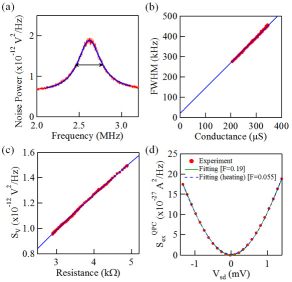
In order to derive the current noise spectral density at the QPC, the noise measurement system was carefully calibrated. Figure 2(b) shows the full width at half maximum (FWHM) of the resonance peak as a function of the device conductance. The impedance originating from the circuit and the capacitance at the resonance frequency were extracted from linear fitting as , respectively DiCarloRSI2006 ; HashisakaPRB2008 , to yield and . In addition, when the cryogenic amplifier involves finite voltage and current noises , the observed for the sample with the circuit resistance is related to as . Here, is the total gain of the amplifiers. Resistance consists of that of the QPC, the Hall bar, and the contacts. By changing the QPC resistance by tuning , we obtain as a function of as shown in Fig.2(c), from which , , and are deduced. Finally, to derive the shot noise and the QPC resistance from the observed and , the contribution of the Hall bar and the contact resistances was taken into account.
Figure 2(d) shows the typical excess noise obtained at as a function of , where corresponds to . is the current noise at the QPC whose thermal noise is subtracted. shows a parabolic behavior around for , which is the crossover from thermal to shot noise ( is the Boltzmann constant). At higher , the excess noise is linearly dependent on . We performed the numerical fitting to obtain the Fano factor by using the following conventional formula BlanterPR2000 :
| (1) |
The solid curve in Fig.2(d) is the result of the fitting, which yields . This Fano factor is deviated from that expected theoretically (), which we discuss later [see dashed curve in Fig. 2(d)]. However, for the moment, we first look at the qualitative aspect of what the experimental result tells. Figure 3(a) shows the Fano factor as a function of , which reduces at the conductance plateaus of . Importantly, although the plateaus are not as perfectly flat as those usually observed in the InGaAs-based QPCs, the reduction of at each plateau is unambiguous. This is the evidence that the shot noise suppresses due to the quantized coherent channel formation in the InGaAs-based QPC.
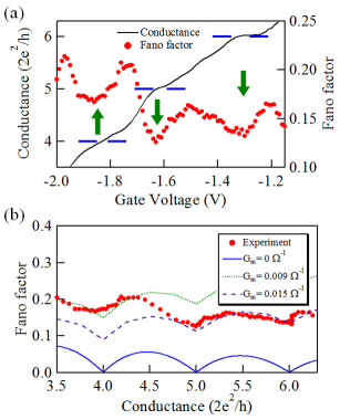
Ideally, no electrons can be reflected at the QPC at the conductance plateaus, leading to the absence of the shot noise, namely, . Our observation, however, shows that the Fano factor remains finite even at the plateaus. Figure 3(b) represents the Fano factor as a function of . The solid curve is the theoretical Fano factor, which is predicted to be , where indicates the transmission probability of the -th quantized channel BlanterPR2000 ; ButtikerPRB1992 ; MartinPRB1992 . Clearly, the experimentally obtained is larger than the theoretical prediction.
There are three possibilities to be responsible for the observed enhancement, namely, the electron heating, the channel mixing, and the noise. Among them, the first one is the most likely. We follow the modelKumarPRL1996 that treats the electron heating as the diffusion by Wiedemann-Franz thermal conduction of the heat flux on both sides of the QPC and of Joule heating in the reservoirs, with the assumption that the ohmic contacts thermalized to the lattice at the system temperature . In this model, the electron temperature () is expressed as . is the parallel conductance of the reservoirs that connect to the QPC. Figure 2(d) shows the simulated shot noise with and , which almost overlaps with the result without heating effect with . The dashed curves in Fig.3(b) are the simulation results with , which typically gives at . Thus, the observed Fano factor can be explained by choosing around these values, which are consistent with the previous report KumarPRL1996 . Although a single fixed value of cannot explain the whole experimental result, the channel mixing would explain it but a quantitative treatment including the mixing effect is difficult KumarPRL1996 . We also note that a satisfying agreement between the experimental result and the simulation in Fig.2(d) strongly suggests the irrelevance of the noise contribution; if the noise would be significant, the excess noise would increase in proportional to so that the simulation could not explain the experimental result. Also, usually, the contribution of the noise would be very drastic as reported before DekkerPRL1991 .
To conclude, we found that the shot noise is reduced at the conductance plateau of the QPC on the InGaAs/InGaAsP heterostructure, which is the direct evidence of the coherent quantized channel formation in this system. The deviation of the Fano factor from the theory was mainly attributed to the electron heating effect. Our achievement suggests that what has been realized in GaAs-based materials is also applicable in InGaAs systems, which, unlike GaAs-based systems, uniquely possess large -factor and strong SOI. Since the shot noise is apowerful tool to study quantum spin transport, further experimental efforts, for example, testing various theoretical predictions FevePRB2002 ; EguesPRL2002 ; AvishaiPRL2010 ; GovernalePRB2003 , will open up the possibilities of InGaAs-based devices in quantum information and spintronics fields.
This work is partially supported by JSPS Funding Program for Next Generation World-Leading Researchers.
References
- (1) S. Murakami, N. Nagaosa, and S. C. Zhang, Science 301, 1348 (2003).
- (2) Y. K. Kato, R. C. Myers, A. C. Gossard, and D. D. Awschalom, Science 306, 1910 (2004).
- (3) S. Datta and B. Das, Appl. Phys. Lett. 56, 665 (1989).
- (4) T. Koga, Y. Sekine, and J. Nitta, Phys. Rev. B 74, 041302(R) (2006).
- (5) J. Ohe, M. Yamamoto, T. Ohstuki, and J. Nitta, Phys. Rev. B 72, 041308(R) (2005).
- (6) S. Nadj-Perge, S. M. Frolov, E. P. A. M. Bakkers, and L. P. Kouwenhoven, Nature (London) 468, 1084-1087 (2010).
- (7) J. Nitta, T. Akazaki, H. Takayanagi, and T. Enoki, Phys. Rev. Lett. 78, 1335 (1997).
- (8) T. Koga, J. Nitta, H. Takayanagi, and S. Datta, Phys. Rev. Lett. 88, 126601 (2002).
- (9) B. J. van Wees, H. van Houten, C. W. J. Beenakker, J. G. Williamson, L. P. Kouwenhoven, D. van der Marel, and C. T. Foxon, Phys. Rev. Lett. 60, 848 (1988).
- (10) D. A. Wharam, T. J. Thornton, R. Newbury, M. Pepper, H. Ahmed, J. E. F. Frost, D. G. Hasko, D. C. Peacockt, D. A. Ritchie, and G. A. C. Jones, J. Phys. C 21, L209 (1988).
- (11) S. Datta, Electronic Transport in Mesoscopic Systems (Cambridge University Press, Cambridge, England, 1995).
- (12) T. Bergsten, T. Kobayashi, Y. Sekine, and J. Nitta, Phys. Rev. Lett. 97, 196803 (2006).
- (13) P. Debray, S. M. S. Rahman, J. Wan, R. S. Newrock, M. Cahay, A. T. Ngo, S. E. Ulloa, S. T. Herbert, M. Muhammad, and M. Johnson, Nat. Nanotechnol. 4, 759-764 (2009).
- (14) M. Kohda and J. Nitta, Phys. Rev. B 81, 115118 (2010).
- (15) G. Engels, J. Lange, Th. Schäpers, and H. Lüth, Phys. Rev. B 55, R1958-R1961 (1997).
- (16) Ya. M. Blanter and M. Büttiker, Phys. Rep. 336, 1 (2000).
- (17) C. Dekker, A. J. Scholten, F. Liefrink, R. Eppenga, H. van Houten, and C. T. Foxon, Phys. Rev. Lett. 66, 2148 (1991).
- (18) M. Reznikov, M. Heiblum, H. Shtrikman, and D. Mahalu, Phys. Rev. Lett. 75, 3340 (1995).
- (19) A. Kumar, L. Saminadayar, D. C. Glattli, Y. Jin, and B. Etienne, Phys. Rev. Lett. 76, 2778 (1996).
- (20) G. Feve, W. D. Oliver, M. Aranzana, and Y. Yamamoto, Phys. Rev. B 66, 155328 (2002).
- (21) J. C. Egues, G. Burkard, and D. Loss, Phys. Rev. Lett. 89, 176401 (2002).
- (22) T. P. Martin, C. A. Marlow, L. Samuelson, A. R. Hamilton, H. Linke, and R. P. Taylor, Phys. Rev. B 77, 155309 (2008).
- (23) Th. Schäpers, V. A. Guzenko, and H. Hardtdegen, Appl. Phys. Lett. 90, 122107 (2007).
- (24) P. J. Simmonds, F. Sfigakis, H. E. Beere, D. A. Ritchie, M. Pepper, D. Anderson, and G. A. C. Jones, Appl. Phys. Lett. 92, 152108 (2008).
- (25) M. Kohda, S. Nakamura, Y. Nishihara, K. Kobayashi, T. Ono, J. Ohe, Y. Tokura, T. Mineno, and J. Nitta, gRashba spin-orbit coupled spin polarization in a quantum point contact h (unpublished).
- (26) S. Nakamura, Y. Yamauchi, M. Hashisaka, K. Chida, K. Kobayashi, T. Ono, R. Leturcq, K. Ensslin, K. Saito, Y. Utsumi, and A. C. Gossard, Phys. Rev. Lett. 104, 080602 (2010).
- (27) Y. Yamauchi, K. Sekiguchi, K. Chida, T. Arakawa, S. Nakamura, K. Kobayashi, T. Ono, T. Fujii, and R. Sakano, Phys. Rev. Lett. 106, 176601 (2011).
- (28) L. DiCarlo, Y. Zhang, D. T. McClure, C. M. Marcus, L. N. Pfeiffer, and K. W. West, Rev. Sci. Instrum. 77, 073906 (2006).
- (29) M. Hashisaka, Y. Yamauchi, S. Nakamura, S. Kasai, T. Ono, and K. Kobayashi, Phys. Rev. B 78, 241303R (2008).
- (30) M. Büttiker, Phys. Rev. B 46, 12485 (1992).
- (31) T. Martin and R. Landauer, Phys. Rev. B 45, 1742 (1992).
- (32) Y. Avishai, D. Cohen, and N. Nagaosa, Phys. Rev. Lett. 104, 196601 (2010).
- (33) M. Governale, F. Tadde, and R. Fazio, Phys. Rev. B 68, 155324 (2003).