Gate defined zero- and one-dimensional confinement in bilayer graphene
Abstract
We report on the fabrication and measurement of nanoscale devices based on bilayer graphene sandwiched between hexagonal boron nitride bottom and top gate dielectrics. The top gates are patterned such that constrictions and islands can be electrostatically induced by applying appropriate voltages to the gates. The high quality of the devices becomes apparent from conductance quantization in the constrictions at low temperature. The islands exhibit clear Coulomb blockade and single-electron transport.
Confinement of charge carriers in graphene has been heavily investigated since graphene flakes on a substrate were first measured.Geim (2009); Neto et al. (2009) Nanopatterning graphene into nanoribbons or small islands has been a widely used strategy for both zero- and one-dimensional confinement.Ponomarenko et al. (2008); Han et al. (2010); Liu et al. (2009); Stampfer et al. (2008); Molitor et al. (2009) Unfortunately, as a result of the etching process that is used for nanopatterning, the edges of the devices are very rough. This edge disorder, aggravated by substrate-induced disorder, leads to rather irregular device behaviour. For instance no quantized conductance was observed in etched constrictions, the transparency of barriers varied non-monotonously with gate voltage, no atom-like shell-filling has been observed in quantum dots and in many cases quantum dots fell apart into multiple islands.
Last year, suspended single layer graphene sheets narrowed by current induced heating showed quantized steps in conductance of as the Fermi wavelength was varied.Tombros et al. (2011) Presumably these constrictions were not only narrow but also short, as observed in recent transmission electron microscope measurements Barreiro et al. (2012), reducing the effects of edge disorder. However, the formation of these constrictions is hard to control, making it difficult to reproduce these results. Clean ribbon edges can be obtained reproducibly by unzipping carbon nanotubes, and a well-behaved quantum dot formed in such a nanoribbon was recently reported.Wang et al. (2011) Barriers were formed at metal Schottky contacts, but such barriers are not tunable, limiting follow-up work. Moreover, as the ribbons are not obtained lithographically but are dispersed from solution, they face many of the limitations of the carbon nanotube they originate from.
The ideal device would confine charge carriers in the bulk, far from (disordered) edges, have well controlled tunnel barriers, and enjoy all the design freedom offered by lithography. All these requirements can be satisfied using patterned electrostatic gates, provided a band gap is present. This calls for the use of bilayer graphene rather than monolayer graphene, as in bilayers a band gap can be induced by an electric field perpendicular to the layers.McCann et al. (2007); Oostinga et al. (2008); Castro et al. (2007) An additional requirement for clean confinement is to minimize substrate-induced disorder. Substrate disorder can be eliminated in suspended devices with suspended top gates, as shown in recent work by Allen et al.Allen et al. (2012) However, it would be highly desirable to realize devices of comparable quality on a substrate, as this would facilitate integration of complex devices. Currently the cleanest gate dielectric available for graphene devices is hexagonal boron nitride (hBN), and mobilities reported on such substrates approach those of suspended devices.Dean et al. (2010)
Here we report 1-dimensional and 0-dimensional electrostatic confinement in bilayer graphene sandwiched in hBN dielectrics. The devices have split top gates and a global back gate, which we bias so that a gap is opened. The Fermi level is tuned inside the gap in the regions below the top gates so that they become insulating. Depending on the combination of top gates that is biased, we form 1-dimensional channels or 0-dimensional islands.
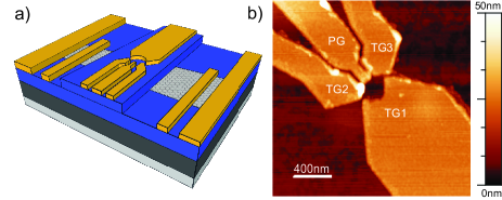
A schematic and AFM image of a device is shown in Fig. 1. We first deposit a nm thick hBN flake by mechanical exfoliation on a silicon wafer coated with a silicon oxide (SiO2) layer of thickness nm. On top of the hBN we transfer a bilayer graphene flake (m long and m wide, its bilayer nature was confirmed by Raman spectroscopy) using a dry transfer method following the protocol of Dean et al. (2010) (at a temperature of C to remove any water absorbed on the surface of the graphene and hBN flakes). The sample was subsequently annealed in an oven at and C (Ar sccm, H2 sccm) to remove residues induced by the transfer process. Cr( nm)/Au( nm) electrodes are fabricated using electron-beam lithography (EBL). We annealed the samples again (same flow rate as the first annealing step, T = , and C) to remove fabrication residues. This did not give the desired sample quality. Hence we applied the recently developed mechanical cleaning technique Goossens et al. (2012) followed by dry transfer of a nm thick hBN flake, which will act as top gate dielectric. In a two-step EBL process we deposited Cr/Au top gates. We defined several gate patterns between the contacts on this flake and report here on two ’quantum dot’ top gate structures, one with a lithographic diameter of nm (device A) and one of nm (device B). The separation between the top gates that together define a barrier is less than nm. For device B, TG1 and TG2 were unintentionally connected.
This specific graphene sample was cooled down multiple times. The maximum overall mobility measured at T= mK was cm2/Vs (four-terminal configuration). The overall mobility measured during the last cool-down was much lower ( cm2/Vs, two-terminal configuration). This degradation of electronic quality was caused by exposure to an electron beam during imaging in a scanning electron microscope. Nevertheless we believe that the graphene sandwiched in hBN remained of high quality.
We set the back gate to a large negative voltage and tune the top gate to a voltage that compensates for the doping induced by the back gate. For typical values V and V the displacement field is V/nm, which translates into a theoretically predicted band gap of meV.McCann et al. (2007); Min et al. (2007); Zhang et al. (2009) As in earlier work, the transport gap is substantially smaller Oostinga et al. (2008); Taychatanapat and Jarillo-Herrero (2010) but still large enough to realize quantum confinement, as we will see.
In Fig. 2a we show a top gate trace at a large negative back gate voltage, taken at low temperature. Clearly visible is a region of suppressed conductance, with a remarkably clean transition region on the hole side, and a somewhat less clean transition and lower conductance on the electron side. This behavior can be expected since the leads are p-doped by the backgate, and a pnp-junction is formed on the electron side. The pnp-junction decreases the transparency of the device as the charge carriers have to Zener tunnel through the induced band gap. On the hole side the conductance suppression with top gate voltage is very smooth and well behaved. This is in strong contrast to similar top gate sweeps for graphene nanoribbons, which exhibit very irregular pinch-off characteristics when the Fermi energy is swept into the transport gap.Han et al. (2010); Molitor et al. (2009); Liu et al. (2009)
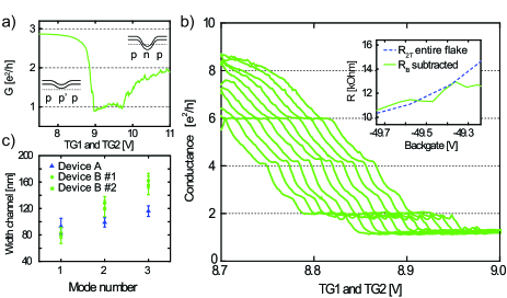
Zooming in on the steep flank of the pinch-off curve, we observe several plateaus in conductance, with a value that is independent of (Fig. 2b). The traces have been corrected for filter resistance, current amplifier input resistance and for a background resistance () consisting of contact resistance, Maxwell spreading resistance and graphene lead resistance. The last two terms are dependent on back gate voltage. For each value of we subtracted a value of comparable to the two-terminal resistance () of the graphene flake with all top gates at ground (see inset fig. 2b), fine tuning such that the conductance at the upper plateau is .111Other choices of compatible with gave either unphysical results, such as negative resistances, or quantized conductance values that we consider highly unlikely, such as plateaus at 8, 5 and 3 times . Subtracting a parallel conductance of , the value of the minimum conductance in the measurement, also gave unlikely conductance plateau values. The other two plateaus consequently appear at and . The same sequence of steps was observed for device A. (in device B, a less well developed feature can be seen just below , which does not appear in device A; its origin is unclear) This behavior is consistent with transport through one-dimensional ballistic channels and the formation of a quantum point contact.Van Wees et al. (1988a); Wharam et al. (1988)
The steps in conductance are surprising given that there is both spin and valley degeneracy in bulk bilayer graphene, so steps are expected. The same observation was recently made on suspended gate-defined bilayer constrictions Allen et al. (2012) but it remains to be understood. Increasing the temperature to 440 mK did not change the general behavior. Lowering the bias to V (lock-in measurement with an AC excitation of 10 V) did not change the appearance of the plateaus either. Both a larger bias and a higher temperature smoothened out universal conductance fluctuations, as can be expected.
We can estimate the width of the constriction from the position of the plateaus in top gate voltage with respect to the conductance minimum (Fig. 2c). We see that as subbands become occupied, the width of the constriction increases from nm to nm for device A and from to nm for device B, which is characteristic of a smooth confining potential (with the constriction width for the -th subband). The lithographically defined separation between the respective top gates was less than nm for both devices. This implies that the channel extends below the top gates, which can be expected given the modest band gap induced underneath.
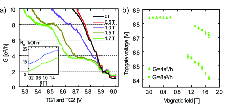
In Fig. 3a we explore the influence of a perpendicular magnetic field on the 1D channels (device B). In the low-field regime, the plateau at quickly disappears, but the plateaus at and remain visible. At large fields, plateaus in conductance develop at () and (), typical values for the quantum Hall effect in bilayer graphene.Novoselov et al. (2006) This transition from size confinement to magnetic confinement occurs when the cyclotron radius () is equal to or larger than .Van Wees et al. (1988b) By extrapolating the positions of the plateaus for and , we can determine a cross-over magnetic field of T and estimate the size of the constriction based on (Fig. 3b). This gives nm. The agreement with the estimate based on the plateau positions ( nm) is better than a factor two.
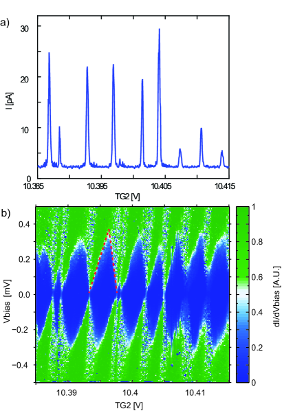
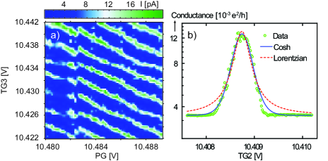
When we induce two barriers by appropriate gate voltages, the device behaviour changes drastically. Fig. 4a shows a gate voltage scan of TG2 while TG1 and TG3 are also biased (device A). We see sharp conductance peaks separated by regions of strongly suppressed conductance, which is characteristic of Coulomb blockade.Kouwenhoven et al. (2001) As expected for Coulomb peaks, their position on one gate voltage axis varies smoothly (linearly) when another gate voltage is swept (Fig. 5a). We note that the resistance in Coulomb blockade is orders of magnitude larger than the sum of the two barrier resistances, which saturates around (Fig. 2), indicating each gate couples to both barriers. Coulomb blockade is confirmed further by the diamond-shaped regions of suppressed conductance seen in a color plot of conductance versus gate voltage and bias voltage (Fig. 4b).
The Coulomb peak spacing exhibits a standard deviation of mV, compared to an average peak spacing of mV (device B). Irregular peak spacings can, in principle, originate from quantized level spacing contributions.Kouwenhoven et al. (2001) However, no excited state features are visible in the Coulomb diamonds so it is not clear that level spacing is responsible for the peak spacing variation. Instead the reason may be the breakdown of the constant-interaction model, for instance due to disorder-induced variations in the island size or position as charge carriers are added one by one, or a second island capacitively coupled to the main island.
From the Coulomb diamonds and peak spacing we can obtain information on the dimensions and location of the island. For the dataset of Fig. 4b (device A), the addition energy is meV. When we neglect orbital energies, , where is the charging energy. Using , we can calculate the total capacitance of the dot, fF. From the slope of the Coulomb diamond edges, we find that is dominated by the source and drain capacitances ( fF, fF), which makes it difficult to estimate the island size from and .
Instead, we compare the measured top gate capacitances with top gate capacitances simulated using a 3D Poisson equation solver (Ansoft Maxwell). From the average Coulomb peak spacing we extract a capacitance aF. , and are comparable. The calculated capacitance between a circular island of nm in diameter and a metal plate with a nm hole, nm above the island, is aF, about as large as each measured top gate capacitance by itself. We thus infer that the island is formed in the central region uncovered by the top gates and extends underneath all the gates. This is consistent with the quantum point contacts extending underneath the split gates as discussed above (see also Allen et al. (2012)). Presumably lateral confinement is less tight in these devices than in GaAs split gate devices, due to the much smaller band gap.
Finally, we investigate whether the dot is weakly or strongly tunnel coupled to the leads by inspecting the line shape of the Coulomb peaks at low bias voltage. In Fig. 5b, we overlay on the data a fit by a hyperbolic cosine function and by a Lorentzian function. The former fits the data much better, indicating that the dot is in the weakly coupled regime, where temperature determines the linewidth rather than tunnel coupling to the reservoirs.Beenakker (1991) Doing the same analysis for 50 peaks we find that they are consistently in the weakly coupled regime. We extract an electron temperature of mK.
Concluding, we show evidence for one-dimensional and zero-dimensional confinement in substrate supported bilayer graphene split gate devices. Transport through a single-barrier device shows signs of conductance quantization and in double-barrier devices clear Coulomb blockade is observed. Further development of this platform will enable us to study the rich physics of quantum confined charge carriers in bilayer graphene. Questions to be addressed include how electron-electron and electron-phonon interactions, and spin and valley lifetimes are modified by the confinement.
We acknowledge useful discussions with A. Akhmerov, A. Barreiro, V. Calado, C. Dean, P. Kim, L. Kouwenhoven, N. Tombros, B. van Wees, M. Wimmer, A. Young and P. Zomer and financial support from the Foundation for Fundamental Research on Matter (FOM) and the European Research Council (ERC Starting Grant).
References
- Geim (2009) A. K. Geim, Science 324, 1530 (2009).
- Neto et al. (2009) A. H. C. Neto, F. Guinea, N. M. R. Peres, K. S. Novoselov, and A. K. Geim, Rev. Mod. Phys. 81, 109 (2009).
- Ponomarenko et al. (2008) L. A. Ponomarenko, F. Schedin, M. I. Katsnelson, R. Yang, E. W. Hill, K. S. Novoselov, and A. K. Geim, Science 320, 356 (2008).
- Han et al. (2010) M. Y. Han, J. C. Brant, and P. Kim, Phys. Rev. Lett. 104, 056801 (2010).
- Liu et al. (2009) X. Liu, J. B. Oostinga, A. F. Morpurgo, and L. M. K. Vandersypen, Phys. Rev. B 80, 121407 (2009).
- Stampfer et al. (2008) C. Stampfer, E. Schurtenberger, F. Molitor, J. Gẗtinger, T. Ihn, and K. Ensslin, Nano Lett. 8, 2378 (2008).
- Molitor et al. (2009) F. Molitor, A. Jacobsen, C. Stampfer, J. Güttinger, T. Ihn, and K. Ensslin, Phys. Rev. B 79, 075426 (2009).
- Tombros et al. (2011) N. Tombros, A. Veligura, J. Junesch, M. H. D. Guimaraes, I. J. Vera-Marun, H. T. Jonkman, and B. J. Van Wees, Nat. Phys. 7, 697 (2011).
- Barreiro et al. (2012) A. Barreiro, F. Börrnert, M. H. Rümmeli, B. Büchner, and L. M. K. Vandersypen, Nano Lett. 12, 1873 (2012).
- Wang et al. (2011) X. Wang, Y. Ouyang, L. Jiao, H. Wang, L. Xie, J. Wu, J. Guo, and H. Dai, Nat. Nano 6, 563 (2011).
- McCann et al. (2007) E. McCann, D. S. Abergel, and V. I. Fal’ko, The European Physical Journal - Special Topics 148, 91 (2007).
- Oostinga et al. (2008) J. B. Oostinga, H. B. Heersche, X. Liu, A. F. Morpurgo, and L. M. K. Vandersypen, Nat. Mater. 7, 151 (2008).
- Castro et al. (2007) E. V. Castro, K. S. Novoselov, S. V. Morozov, N. M. R. Peres, J. M. B. L. dos Santos, J. Nilsson, F. Guinea, A. K. Geim, and A. H. C. Neto, Phys. Rev. Lett. 99, 216802 (2007).
- Allen et al. (2012) M. T. Allen, J. Martin, and A. Yacoby, arXiv:1202.0820 (2012).
- Dean et al. (2010) C. Dean, A. Young, I. Meric, C. Lee, L. Wang, S. Sorgenfrei, K. Watanabe, T. Taniguchi, P. Kim, K. Shepard, and J. Hone, Nat. Nano 5, 722 (2010).
- Goossens et al. (2012) A. M. Goossens, V. E. Calado, A. Barreiro, K. Watanabe, T. Taniguchi, and L. M. K. Vandersypen, Appl. Phys. Lett. 100, 073110 (2012).
- Min et al. (2007) H. Min, B. Sahu, S. K. Banerjee, and A. H. MacDonald, Phys. Rev. B 75, 155115 (2007).
- Zhang et al. (2009) Y. Zhang, T. Tang, C. Girit, Z. Hao, M. C. Martin, A. Zettl, M. F. Crommie, Y. R. Shen, and F. Wang, Nature 459, 820 (2009).
- Taychatanapat and Jarillo-Herrero (2010) T. Taychatanapat and P. Jarillo-Herrero, Phys. Rev. Lett. 105, 166601 (2010).
- Note (1) Other choices of compatible with gave either unphysical results, such as negative resistances, or quantized conductance values that we consider highly unlikely, such as plateaus at 8, 5 and 3 times . Subtracting a parallel conductance of , the value of the minimum conductance in the measurement, also gave unlikely conductance plateau values.
- Van Wees et al. (1988a) B. J. Van Wees, H. Van Houten, C. W. J. Beenakker, J. G. Williamson, L. P. Kouwenhoven, D. van der Marel, and C. T. Foxon, Phys. Rev. Lett. 60, 848 (1988a).
- Wharam et al. (1988) D. A. Wharam, T. J. Thornton, R. Newbury, M. Pepper, H. Ahmed, J. E. F. Frost, D. G. Hasko, D. C. Peacock, D. A. Ritchie, and G. A. C. Jones, J. Phys. C: Solid State Phys. 21, L209 (1988).
- Novoselov et al. (2006) K. S. Novoselov, E. McCann, S. V. Morozov, V. I. Fal’ko, M. I. Katsnelson, U. Zeitler, D. Jiang, F. Schedin, and A. K. Geim, Nat. Phys. 2, 177 (2006).
- Van Wees et al. (1988b) B. J. Van Wees, L. P. Kouwenhoven, H. van Houten, C. W. J. Beenakker, J. E. Mooij, C. T. Foxon, and J. J. Harris, Phys. Rev. B 38, 3625 (1988b).
- Kouwenhoven et al. (2001) L. P. Kouwenhoven, D. G. Austing, and S. Tarucha, Rep. Prog. Phys. 64, 701 (2001).
- Beenakker (1991) C. W. J. Beenakker, Phys. Rev. B 44, 1646 (1991).