Light scattering by a medium with a spatially modulated optical conductivity: the case of graphene
Abstract
We describe light scattering from a graphene sheet having a modulated optical conductivity. We show that such modulation enables the excitation of surface plasmon-polaritons by an electromagnetic wave impinging at normal incidence. The resulting surface plasmon-polaritons are responsible for a substantial increase of electromagnetic radiation absorption by the graphene sheet. The origin of the modulation can be due either to a periodic strain field or to adatoms (or absorbed molecules) with a modulated adsorption profile.
pacs:
81.05.ue,72.80.Vp,78.67.Wj1 Introduction
Since the days of A. Sommerfeld, back to 1899, that plasmonics effects in materials and gratings are investigated both theoretically and experimentally. Modern plasmonics gained a renewed interest with the discovery super transmittance through a periodic array of holes with a size smaller than the diffraction limit [1]. The effect was explained invoking surface plasmons (SPs) [2, 3, 4, 5]. Beyond fundamental physics, plasmonics encompasses wide range of applications, such as spectroscopy and sensing [6, 7, 8], photovoltaics [9], optical tweezers [10, 11], nano-photonics [12, 3], transformation optics [13], etc.
A series of recent papers [14, 15, 16] triggered a burst of interest on plasmonic effects in graphene. In particular, it has been shown that graphene has a strong plasmonic response in the THz frequency range at room temperature [15]. THz photonics is emerging as an active field of research [17] and graphene may play a key role in THz metamaterials in the near future. Ju et al. [15] has shown that electromagnetic radiation impinging on a grid of graphene micro-ribbons can excite SPs on graphene leading to prominent absorption peaks, whose position can be tuned by doping. In general, SPs cannot be excited by directly shining light in a homogeneous system due to kinematic reasons: the momentum of a SP is much larger than that of the incoming light having the same frequency. Therefore some type of mechanism is necessary to promote the excitation of surface plasmons. The most common mechanisms for SP excitation are: attenuated total reflection (ATR) [18], scattering from a topological defect at the surface of the metal [3], and Bragg scattering using diffraction gratings (or producing a periodic corrugation) on the surface of the conductor [19]. The method of Ju et al. is similar (but not exactly) to patterning a metallic grating [16] on top of graphene. A theoretical account of the experiment by Ju et al. [15] was given in a recent work [20].
The reason why a periodic corrugation allows the excitation of SPs can be understood by an analogy with the theory of electrons in a periodic potential. The corrugation plays the role of the periodic potential. Therefore, the SP momentum is conserved up to a reciprocal lattice vector, that is to say, the periodic corrugation provides the missing momentum needed to excite the SP. Another way of seeing the effect is to note that the grating gives rise to a SP band structure in the first Brillouin zone. Then, the folding to plasmonic bands makes it possible to the impinging light to excite a SP associated with the upper bands in the Brilloun zone. The excitation of SP modes in the first band is not possible in the grating configuration unless the ATR technique is used.
The question we want to answer in this article is the following: in what circumstances can electromagnetic radiation (ER) impinging at the interface of a dielectric and a metal excite SPs when the surface of the conductor has no corrugation? Taking the example of graphene, we show that a periodic modulation of the conductivity suffices for that end. In situations where both modulation of the conductivity and corrugation are present, understanding the former situation alone is a needed research step.
2 Modulated conductivity
Several procedures can be used to induce a patterned conductivity on a graphene sheet. One way is using split gates [21]. This leads to a modulation in the electronic density which induces a modulation of the conductivity. One can also assume that a CVD grown graphene sheet is transferred onto a patterned substrate, as illustrated in Fig. 1. The transfer process together with the patterning act in a way to produce inhomogeneous strain in the graphene sheet. Qualitatively, we expect the strain to be higher in regions labeled by 1 in Fig. 1 than in those labeled by 2.
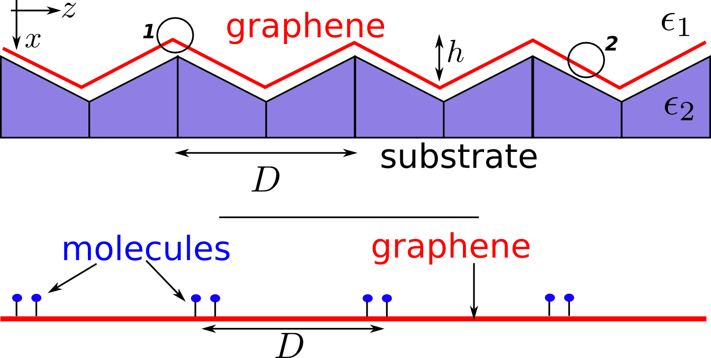
In a typical experiment we have . In this regime we can safely neglect the effect of the groves in what concerns electromagnetic radiation scattering. Due to strain, the optical conductivity of graphene will be spatially modulated with the period of the patterned substrate. Naturally, the form of the modulated conductivity depends on the strain field. It is a rather complex problem to determine the exact form of the spatial conductivity, mainly because the strain field is not known exactly. In any case, we can say that the strain field should have the same period of the patterned substrate.
Another possibility for producing a modulated conductivity is by molecular adsorption. One can imagine an experimental procedure, for instance using a mask, where graphene has regions exposed to molecular absorption separated from others where the concentration of adsorbates is small. This would produce a modulated electron concentration profile that would generate a modulated conductivity.
For illustrative purposes alone, we model the conductivity of graphene by
| (1) |
where is the conductivity of homogeneous graphene and is related to either the strain field field or the molecular doping concentration. Eq. (1) should be considered a toy model.
The conductivity of graphene is a sum of two contributions: (i) a Drude term, describing intra-band processes and (ii) a term describing inter-band transitions. At zero temperature the optical conductivity has a simple analytical expression [22, 23, 24, 25, 26]. The inter-band contribution has the form , with
| (2) |
and
| (3) |
where . The Drude conductivity term is
| (4) |
where is the relaxation rate and is the (local) Fermi level position with respect to the Dirac point. The total conductivity is
| (5) |
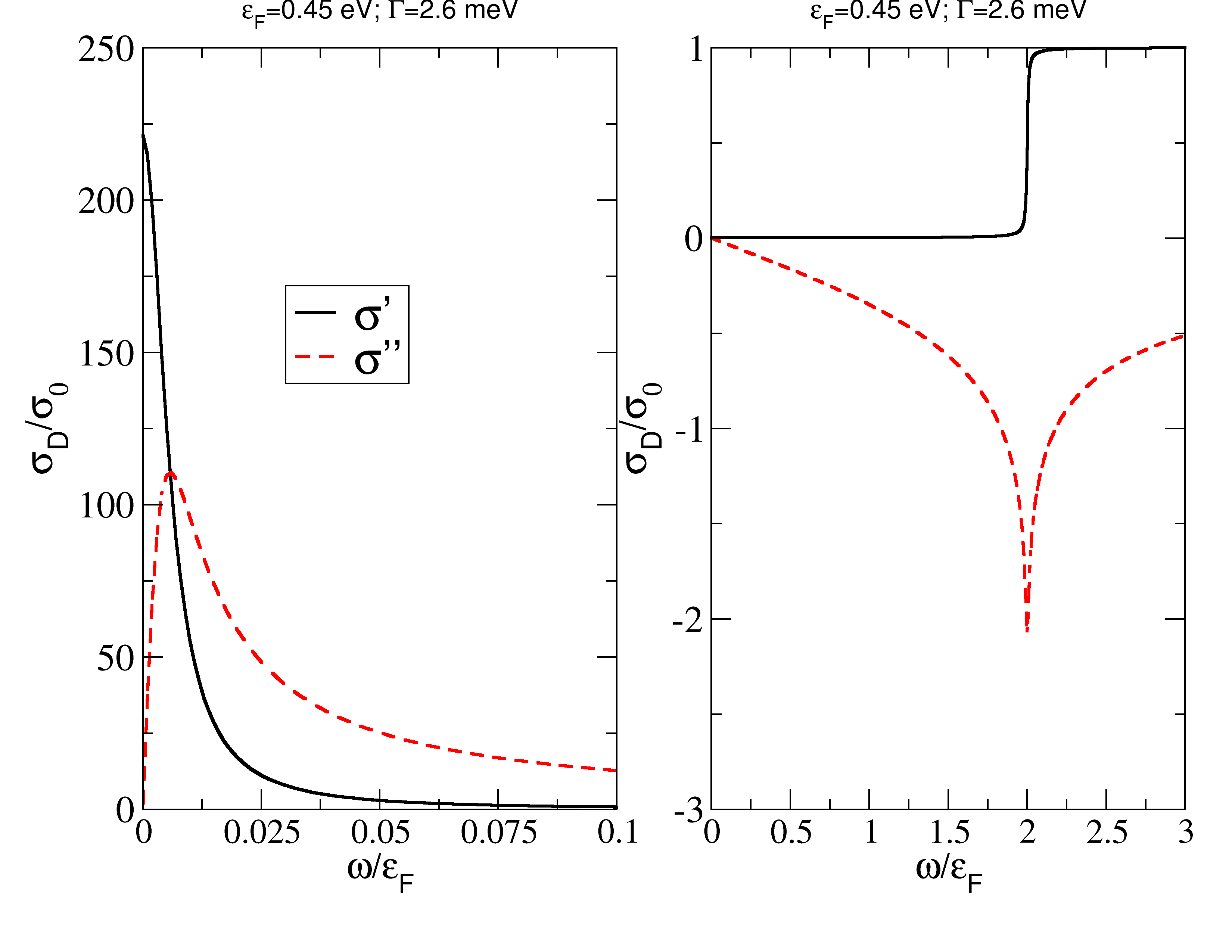
In Fig. 2 we plot the two contributions, Drude and inter-band, separately for a given value of and . For heavily doped graphene and for photon energies the optical response is dominated by the Drude term. Therefore, in what follows we assume
| (6) |
since we are interested in the regime of frequencies . For the frequency range of interest in this work (the THz spectral range) the above approximation gives accurate results. For the simulations given ahead we assume graphene sandwiched between two dielectrics of relative permittivities and , and an average Fermi level 0.45 meV, as in the experiments of Ref. [15]. In the same experiments the array of micro-ribbons has a period of m. In this work we choose m.
3 SPP dispersion
Before solving the problem of ER scattering by a modulated conductivity, we overview some key concepts on surface plasmons-polaritons (SPPs) dispersion relation. SPPs are hybridized modes of electromagnetic radiation and free electrons of a conductor. They propagate along the interface of a dielectric and a conductor, and decay exponentially away from the interface. In the case of graphene, SPPs propagate along the graphene sheet. The SPPs have polarization (TM-wave) and their spectrum is given by [27, 28, 29]:
| (7) |
and
| (8) |
where labels the media 1 (above) and 2 (below) the graphene sheet, is the velocity of light in medium , is the propagation wave number along the interface, and is the permeability of medium (we shall assume that , the value in the vacuum). When the two media are equal, we obtain a simpler relation for the spectrum of the SPPs
| (9) |
The wave number gives the degree of localization of the SPP. This is defined as the ratio (assuming graphene in vacuum) [30]
| (10) |
where is the fine structure constant in free space and we have used Drude’s formula for the conductivity, and took the limit . If we plug in typical numbers (see section ahead) we obtain
| (11) |
meaning a confinement size smaller than the wavelength of light in free space. Depending on the value of the Fermi energy and on the frequency of interest the degree of localization can be much smaller than 1.
In general, Eqs. (7) and (9) cannot be solved analytically. However, approximating by its imaginary part (dispersive conductor approximation)
| (12) |
and taking (for simplicity) , the vacuum value for the permittivity, we obtain
| (13) |
or
| (14) |
In the limit (non-retarded approximation) we obtain for the dispersion relation of the SPP the simple formula
| (15) |
In the limit we find that the SPP dispersion relation tends to . For the case where , the non-retarded approximation yields
| (16) |
where
| (17) |
with . We note that the behaviour of as cannot be trusted at small , because for those values of the non-retarded approximation is violated. In this case a full numerical solution of Eq. (7) is necessary. In what concerns the problem of ER scattering discussed ahead we will always be in the regime where the non-retarded approximation holds.
In Figs. 3 and 4 we present the low momentum behaviour of the SPPs spectrum comparing the numerical solution of Eq. (7) for different levels of approximation to the optical conductivity and considering the role of the damping .

In Fig. 3 the effect of the damping is studied, keeping the full conductivity . In this case the momentum becomes a complex number, , where describes the decay of the SPPs as it propagates in space along the graphene sheet. From this figure we see that the effect of the increase of the damping is two-fold: it shifts the SPPs dispersion relation toward higher energies and enhances the value of (as expected). If one wants to have long propagation lengths for the SPPs must be as small as possible. In the same figure we also represent the light-lines and which are the dispersion relations of a photon propagating in media 1 and 2, respectively. At grazing incidence it is possible to excite SPPs in graphene with a momentum corresponding to the point where the light line intercepts the dispersion curve of the SPPs. This occurs, unfortunately, at very low energies, THz, which corresponds to meV.
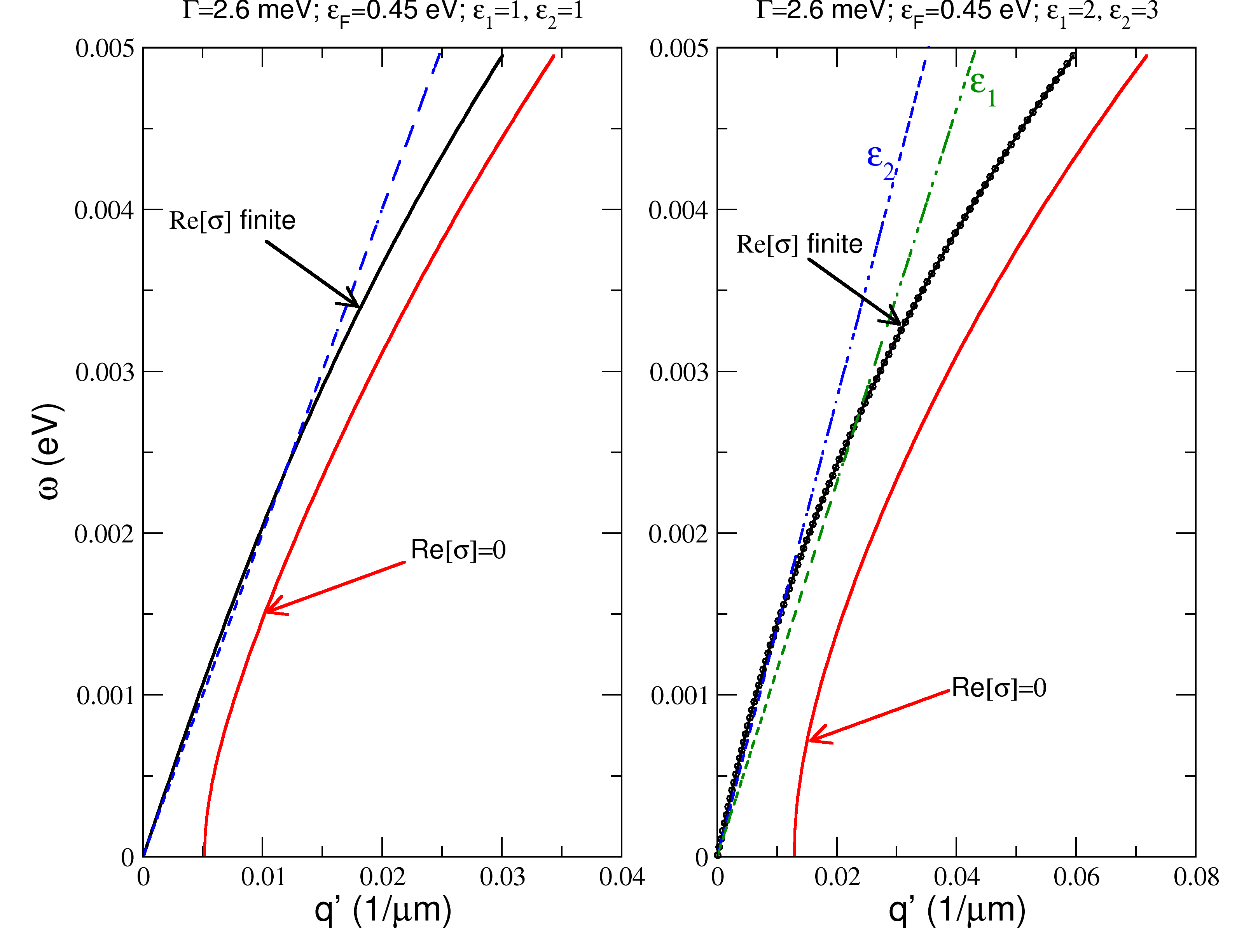
In Fig. 4 we present the effect of neglecting the real part of the optical conductivity. The central feature is the vanishing of the dispersion curve for a finite value of . This is a spurious result: when we use the full Drude conductivity the dispersion vanishes at zero . Changing the dielectric constants of the surrounding media changes the value of for the same frequency, as can be seen comparing the left and right panels of Fig. 4.
When a periodic modulation of the conductivity exists, the SPPs develop a band structure depicted in Fig. 5. The black dashed lines represent the folding of the dispersion curve (16) into the first Brillouin zone, for vanishing modulation of the conductivity (). For finite modulation of () gaps develop at the edges of the Brillouin zone. The band structure represented in Fig. 5 was computed in the non-retarded approximation, considering only the imaginary part of the conductivity (meaning that and ), and taking . As such, the behaviour of the first band close to is not accurate. In this approximation, there are no gaps at the center of the zone. (The approximations used allows to transform a non-linear eigen-problem into a linear one.) The region of the band structure between the two straight lines (see Fig. 5) can be directly excited by light impinging on graphene without the aid of the ATR technique. If ER impinges at an angle , the momentum along the graphene sheet is and then a SPP with momentum can be created. This corresponds to a frequency of
| (18) |
When the straight line (18) intercepts one of the upper bands in the Brillouin zone a SPP can be excited. If the modulation in the conductivity is weak (as, for example, is the case ; see Fig. 5) the energy of the excited SPP is roughly given by
| (19) |
where and an integer.

To conclude this section, we highlight the result we use later in the interpretation of ER scattering: for large the dispersion relation is approximately given by Eq. (16) and at high energies SPPs cannot be excited by shining light on homogeneous graphene, even at grazing incidence. When the optical conductivity is modulated periodically the system develops a band structure for the SPPs dispersion relation and their direct excitation becomes possible.
4 Electromagnetic radiation scattering: formalism
As discussed in Sec. 2 a conductive surface bearing a modulated conductivity supports SPPs which can be directly excited by light impinging on the conductor’s surface, that is, without the need of a grating. We develop now the formalism needed to study, in a quantitative way, ER scattering by a modulated conductivity.
Since the conductivity is a periodic function we can write it as a Fourier series ():
| (20) |
where
| (21) |
Considering polarization, we write the electromagnetic fields as series of Bloch waves
| (22) |
where labels the two cladding media. The relations between the amplitudes of the fields follow from Maxwell’s equations:
-
1.
incoming field ():
(23) (24) -
2.
reflected field ():
(25) (26) -
3.
transmitted field ():
(27) (28)
The boundary condition implies:
| (29) | |||||
| (30) |
The second boundary condition, , implies
| (31) | |||||
| (32) |
Using the relations between fields, Eqs. (24)-(28), the set of boundary conditions reduces to
| (33) | |||||
| (34) |
We note that , with . We further define
| (35) |
for a positive argument of the square root (evanescent waves); if the argument of the square root in Eq. (35) is negative (propagating waves) is written as
| (36) |
The choice of sign for the square root is dictated by physical reasons: reflected waves for and transmitted waves for . The “pseudo-reflectance amplitude” of the mode is defined as
| (37) |
and that of a mode is given by
| (38) |
The reflectance of the order (for propagating modes) reads
| (39) |
The reflectance and the transmittance of the specular () mode are given by
| (40) |
and
| (41) |
respectively. The last expression is valid for or for , the critical angle for total reflection. In what follows only the the specular mode is propagating (all the remaining modes are evanescent). Then, the absorbance is simply given by .
5 Special limits
Here we show that the linear system of Eqs. (33) and (34) reduces to well known formulae when the conductivity of graphene is either zero or finite and homogeneous. If the conductivity of graphene vanishes, we simply have an interface between two different dielectrics. In this case Eqs. (33) and (34) give ()and
| (42) |
The reflectance amplitude follows from
| (43) |
which reproduces the well known result from elementary optics.
Another particular limit is obtained when is finite and homogeneous. In this case, only the Fourier component of exists. Thus, we obtain
| (44) |
For we obtain the well known result for the transmittance of graphene (for a TM wave) [26]
| (45) |
6 Electromagnetic radiation scattering: results
When the optical conductivity of graphene has the form (1), the Fourier transform of reads:
| (46) | |||||
| (47) |
The linear system defined by Eqs. (33) and (34) is solved numerically and the sums over are cutoff at ; the numerical solution rapidly converges with .
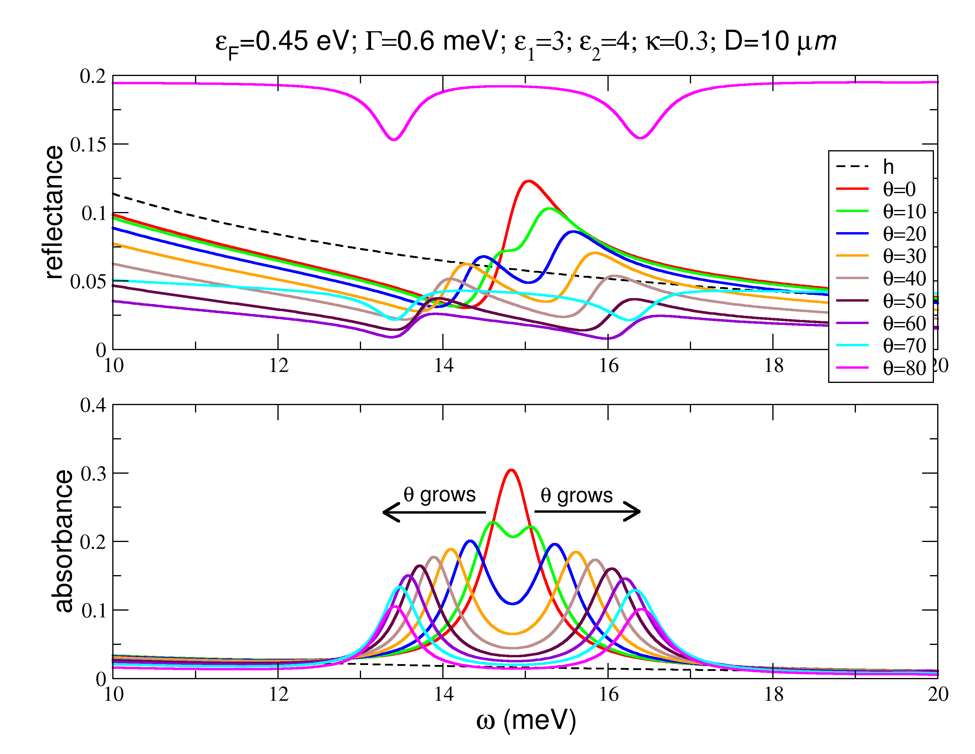
Results for the specular reflectance, , and for the absorbance, , are given in Fig. 6. As discussed in Sec. 3, it is not possible to excite SPPs in a homogeneous system because of the mismatch of the momentum of the incoming ER and that of SPP for the same frequency .
For a modulated conductivity the momentum of the SPPs is conserved up to a reciprocal lattice vector , with , that is
| (48) |
In this case, even for normal incidence, it is possible to excite SPPs. We stress that in the present case it is the periodicity of the conductivity and not an external grating leading to the validity of Eq. (48). The excitation of the SPPs at normal incidence is clearly seen in Fig. 6. In this figure both the reflectance and the absorbance are shown and a clear signature of SPPs excitation is present in both plots. The dashed black curve represents the behaviour of the system for a homogeneous conductivity and impinging ER at normal incidence; clearly the curve is featureless. For the inhomogeneous case a large enhancement of the absorbance is seen around the energy given by Eq. (16) with . The position of the peak does not coincide exactly with the number given by Eq. (16) because this equation is not sensitive to details of the band structure. From Fig. 5 we can see that the bands for at the zone center have an energy of about 15 meV, coinciding with the energy for which the reflectance curve has a maximum for . As the angle of the incident beam approaches the Brewster angle of the two media the reflectivity decreases substantially. The Brewster angle of the system is not given exactly by the well known formula due to the presence of graphene. For incidence angles above the Brewster angle the reflectance develops two dips and can be larger than it would be for (see curve for ).
When the incoming beam deviates from normal incidence (i. e., ), there is a peak splitting both in the reflectance and in the absorbance curves. We would like to understand in qualitative terms the behaviour of the peak slitting as function of the incoming angle . Using Eq. (48) in Eq. (16) yields
| (49) |
with . Clearly, when and increases the frequency shifts toward higher energies. On the other hand, when the energy decreases as increases. This behavior can be understood from the analysis of Fig. 5. For the light line, Eq. (18), is vertical and touches the second band at the center of the zone () where the branches associated with and touch each other. As grows, the slope of light line decreases and the branches with both and are no longer degenerate.
It is possible to obtain a simple analytical expression for by solving Eq. (49) for . The final result is
| (50) |
for and , respectively, and the constants and are given by
| (51) | |||||
| (52) |
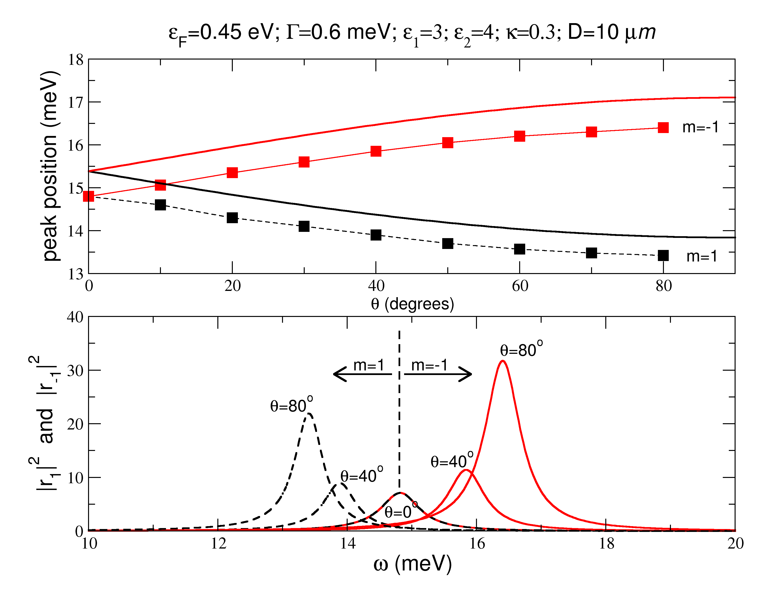
In Fig. 7 we plot the two branches of Eq. (50) and compare it with the position of the peaks for the absorbance obtained from Fig. 6; the agreement is qualitative. It cannot be quantitative because: (i) Eq. (50) is derived from a kinematic argument and, therefore, misses the dependence on ; (ii) we have used the non-retarded approximation. However, for small the agreement is quite good. Indeed, if we had shifted the solid curves in Fig. 7 by a constant, they would overlap the points (solid squares) obtained from Fig. 6. In the bottom panel of Fig. 7 we plot for different as a function of the energy. The energy of the peaks of coincides with that of peaks in the reflectance (and absorbance). This shows that the SPPs associated with the momenta are the ones contributing to the anomalies in the reflectance and absorbance spectra.
7 Conclusions
We have shown that a modulated conductivity in an otherwise flat graphene sheet gives rise to a SPPs band structure with gaps opening at the edges of the Brillouin zone. Within the non-retarded approximation, no gaps open at the center of the zone. This band structure was later used to understand the qualitative behaviour of ER scattering from a flat graphene sheet with a modulated conductivity. The modulation allows for the SPPs be efficiently excited without using the ATR technique. The properties of the studied system resemble those of a photonic crystal. This analogy will be explored in a future work.
If in addition to the modulated conductivity, corrugation is induced in the graphene sheet the reflectance and absorbance spectra are predicted to have a richer structure due to two competing mechanisms: the inhomogeneity and the presence of the groves. Finally we note that the case where graphene is cut into micro-ribbons is qualitatively different from the one discussed here, because the graphene sheet is, in that case, discontinuous.
References
References
- [1] Ebbesen T W, Lezec H J, Ghaemi H F, Thio T and Wolf P A 1998 Nature 391 667
- [2] Barnes W L, Dereux A and Ebbesen T W 2003 Nature 424 824
- [3] Ebbesen T W, Genet C and Bozhevolnyi S I 2008 Phys. Today May 44
- [4] Stockman M I 2011 Phys. Today February 39
- [5] Maier S A 2007 Plasmonics: Fundamentals and Applications (Springer)
- [6] Haes A J, Haynes C L, DMcFarland A, Schatz G C, Van Duyne R P and Zou S 2005 MRS Bulletin 30 368
- [7] Willets K A and Van Duyne R P 2007 Annu. Rev. Phys. Chem. 58 267
- [8] Shalabney A and Abdulhalim I 2011 Laser Photon. Rev. 5 571
- [9] Green M A and Pillai S 2012 Nature Photonics 6 130
- [10] Reece P J 2008 Nature Photonics 2 333
- [11] Juan M L, Righini M and Quidant R 2011 Nature Photonics 5 349
- [12] Ozbay E 2006 Science 311 189
- [13] Vakil A and Engheta N 2011 Science 332 1291
- [14] Schedin F, Lidorikis E, Lombardo A, Kravets V G, Geim A K, Grigorenko A N, Novoselov K S and Ferrari A C 2010 ACSNano 4 5617
- [15] Ju L, Geng B, Horng J, Girit C, Martin M C, Hao Z, Bechtel H A, Liang X, Zettl A, Shen Y R and Wang F 2011 Nature Nanotechnology 6 630
- [16] Echtermeyer T J, Britnell L, Jasnos P K, Lombardo A, Gorbachev R V, Grigorenko A N, Geim A K, Ferrari A and Novoselov K S 2011 Nature Communications 2 458
- [17] Zhang X C and Xu J 2010 Introduction to THz Wave Photonics (Springer)
- [18] Bludov Y V, Vasilevskiy M I and Peres N M R 2010 EPL 92 68001
- [19] Toigo F, Marvin A, Celli V and Hill N R 1977 Phys. Rev. B 15 5618
- [20] Nikitin A Y, Guinea F, Garcia-Vidal F J and Martin-Moreno L 2011 Phys. Rev. B 85 081405
- [21] Davoyan A R, Popov V V and Nikitov S A 2012 Phys. Rev. Lett. 108 127401
- [22] Peres N M R, Guinea F and Castro Neto A H 2006 Phys. Rev. B 73 125411
- [23] Falkovsky L A and Pershoguba S S 2007 Phys. Rev. B 76 153410
- [24] Castro Neto A H, Guinea F, Peres N M R, Novoselov K S and Geim A K 2009 Rev. Mod. Phys. 81 109
- [25] Peres N M R 2010 Rev. Mod. Phys. 82 2673
- [26] Stauber T, Peres N M R and Geim A K 2008 Phys. Rev. B 78 085432
- [27] Falko V I and Khmelnitskii D E 1989 Sov. Phys. JETP 68 1150
- [28] Mikhailov S A and Ziegler K 2007 Phys. Rev. Lett. 99 016803
- [29] Jablan M, Buljan H and Soljačić M 2009 Phys. Rev. B 80 245435
- [30] Koppens F H L, Chang D E and de Abajo F J G 2011 Nano Lett. 11 3370