Giant magneto-optical response in non-magnetic semiconductor BiTeI driven by bulk Rashba spin splitting
Abstract
We study the magneto-optical (MO) response of polar semiconductor BiTeI with giant bulk Rashba spin splitting at various carrier densities. Despite being non-magnetic, the material is found to yield a huge MO activity in the infrared region under moderate magnetic fields ( T). By comparison with first-principles calculations, we show that such an enhanced MO response is mainly due to the intraband transitions between the Rashba-split bulk conduction bands in BiTeI, which give rise to distinct novel features and systematic doping dependence of the MO spectra. We further predict an even more pronounced enhancement in the low-energy MO response and dc Hall effect near the crossing (Dirac) point of the conduction bands.
pacs:
78.20.-e,78.20.Bh,78.20.Ls,71.70.EjThe spin-orbit interaction (SOI) plays a crucial role in the rapidly evolving field of spintronics awschalom ; parkin ; sinova2 ; winkler . The principal importance of SOI is in its ability to intrinsically couple the electron spin with its orbital motion, and hence produce many novel phenomena such as the spin Hall effect murakami and spin Galvanic effect ganicgev . In the presence of an external magnetic field, SOI can effectively mediate the interaction between photons and electron spins, thereby leading to interesting magneto-optical (MO) effects, e.g. non-linear Kerr rotation bennemann whereby the polarization plane of the linearly-polarized light in reflection is rotated as a consequence of SOI.
In practice, most materials under magnetic field exhibit a rather complicated MO response. This is because usually too many energy bands are involved in the optical excitations, which, given that SOI is also at work, leads the respective inter- and intraband optical transitions to produce complex spectra. This accordingly prevents a comprehensive understanding of the role of SOI on the MO response of the given materials using the available theoretical models. In contrast, semiconductors with Rashba-split conduction/valence bands appear to be ideal systems for studying MO effects, as they have a rather simple spin-dependent multi-band scheme. However, these systems have rarely been studied up to now, mainly because they usually show a very weak Rashba spin splitting (RSS) which cannot be resolved experimentally, and also because RSS had been found only in the two-dimensional electron-gas or metallic systems formed at the surface or interface where the MO effect is hardly detectable.
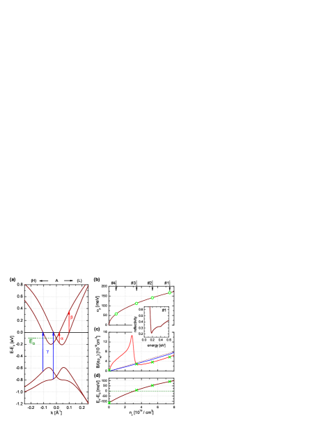
This situation has been greatly improved recently by the discovery of the giant bulk RSS in the polar semiconductor BiTeI. The angle-resolved photoemission spectroscopy (ARPES) bitei_arpes has revealed that the bulk conduction bands in BiTeI are subject to a large RSS (see Fig. 1(a)), well describable by the 2D Rashba Hamiltonian , near the time-reversal symmetry point A, where is the direction of the potential gradient breaking the inversion symmetry, and and are the spin and momentum operators, respectively. This leads to a Dirac-like band dispersion near and a splitting increasing linearly with . The succeeding first-principles calculations bitei_theory ; bitei_pressure and the optical conductivity spectra bitei_sigmaxx have been consistent with the APRES data and further revealed that not only the bottom conduction bands (BCBs) but also the top valence bands (TVBs) are subject to a comparable RSS in BiTeI. This condition allows several distinct inter- and intraband transitions between these two sets of states. The reduced dimensionality together with RSS introduces a well-defined singularity in the joint density of states at the band edge. Therefore, this material is a promising candidate to host the enhanced spin-charge coupling and/or the magnetoelectric effect with the possible applications to spintronics. From this viewpoint, the MO effect is an intriguing issue in BiTeI; the novel interplay between RSS and external magnetic field has been extensively investigated from theoretical side shen ; burkov ; xu ; kushwaha but hardly ever probed experimentally in a real compound. Of particular interest are the states near the band crossing (Dirac) point formed by RSS, as they turn into novel Landau levels under magnetic field similar to the case of graphene shen . Thus, it is important to know their impact on the MO response, e.g. by tuning the Fermi level across the Dirac point. In this Letter, we accordingly study in detail the MO properties of BiTeI both experimentally and theoretically. It is shown that due to giant RSS of bulk bands, the material exhibits a huge enhancement in its MO response in the infrared spectra under a moderately low magnetic field of 3 T. This enhancement is further anticipated to be even more pronounced in the low-energy region near the Dirac point of BCBs.
BiTeI has a trigonal crystal structure with symmetry composed of consecutive Bi, Te, and I layers stacking along the -axis of the crystal bitei_arpes ; bitei_theory . Due to ionicity and covalency of Bi-I and Bi-Te bonds, the bulk material possesses an intrinsic polarity along the -axis which, when coupled with the strong atomic SOI of Bi, leads to a huge bulk RSS. The calculated band structure of BCBs and TVBs around the band gap (along direction), together with the possible inter- and intraband transitions, is shown in Fig. 1(a).
The MO effects are discussed by analyzing the elements of the optical conductivity tensor. For the determination of the off-diagonal components, first the reflectivity spectra were measured over a broad energy range ( meV eV and meV eV at room and low temperatures, respectively); for measurements above eV, the synchrotron radiation from UVSOR at the Institute for Molecular Science, Okazaki, was utilized. The diagonal part has been derived through the Kramers-Kronig transformation. As the second step, the complex magneto-optical Kerr angle was measured by a magneto-optical Kerr effect (MOKE) setup: The combination of a Fourier-transform infrared spectrometer, a polarization modulation technique moke afforded by a ZnSe photoelastic modulator, and a room temperature-bore magnet has enabled the direct derivation of the off-diagonal conductivity via the following relation:
| (1) |
The applicable energy range of the setup is meV. The experiments were carried out in reflection configuration with nearly normal incidence on cleaved surfaces of the -plane. The low-temperature measurements were performed at K, while the external magnetic field of T has been applied perpendicular to the sample surface in the case of the MOKE measurements.
To analyze the respective MOKE data, the longitudinal conductivity has been derived from the Kubo formula as described in bitei_sigmaxx , while the transverse conductivity has been calculated to linear order in the external magnetic field using the Fukuyama formula fukuyama ,
| (2) |
where is the one-particle thermal Green’s function, with , the damping constant, and is obtained from by replacing with ; denotes the electron mass, the volume of the system, and () the velocity operator represented in matrix form as
| (3) |
where corresponds to the th eigenstate of . These matrix elements were computed by downfolding the ab-initio Hamiltonian ab-initio to a low-energy tight binding model, which was constructed for the 12 valence and 6 conduction bands around the band gap bitei_theory . To evaluate the formula (2), the sum over Matsubara frequencies was transformed into a contour integral along the branch cuts of the Green’s functions mahan . After performing the analytic continuation , the contour integral as well as the momentum integral were evaluated numerically. In our calculations, is fixed at meV (this value has already been proven to work well for the analysis of the diagonal conductivity spectrum bitei_sigmaxx ).
The carrier densities of different samples were first estimated from the plasma edge of the free carriers in the ab-plane (depicted in the inset of Fig. 1(b)) using , where is the effective carrier mass, and the high-frequency (background) dielectric constant as determined by the ARPES and previous optical measurements, respectively bitei_arpes ; bitei_sigmaxx . The effect of carrier doping may be treated within the rigid band approximation and then the carrier concentration dependence of the Fermi energy shows a monotonic behavior as plotted in Fig. 1(d). To study the effect of carrier doping on MO response, we targeted the samples with representative carrier concentrations, whose are above (sample #1 and #2), around (#3), and below (#4) the Dirac point. The high-quality single crystal was grown by the chemical vapor transport method and was controlled by the growth conditions for samples #1 and #3. On the other hand, the Bridgman method has been employed as described in bitei_arpes for samples #2 and #4, and has been tuned by doping Sb and Cu, respectively. As indicated in Fig. 1(b) the corresponding carrier densities estimated from the plasma frequencies are 7.5, 5.4, 3.4, and 0.9cm3 for samples #1–4, respectively. Another way to determine the carrier concentration would be via Hall measurements. Importantly, however, in the case of BiTeI the relation does not hold. Figure 1(c) shows the calculated dc Hall response as a function of with and without taking into account SOI, which clearly demonstrates that the conventional Hall data analysis under(over)estimates the carrier density above (below) the Dirac point. The origin of the large enhancement of (or the suppression of ) around the Dirac point is due to the coexistence of electron and hole pockets, or equivalently to the donuts-like Fermi surfaces in the RSS band. In the case of samples #1–3 the results of magnetotransport experiments in conjunction with the calculations can give the carrier density values in accord with the values estimated from the plasma edge (Fig. 1(b)). However, this is not the case for sample #4, where the complex characteristics of the Fermi surface makes the simple estimate based on the plasma frequency less adequate. Consequently, in the following analysis we use cm3 as the carrier density of sample #4 estimated from the realistic band structure model.
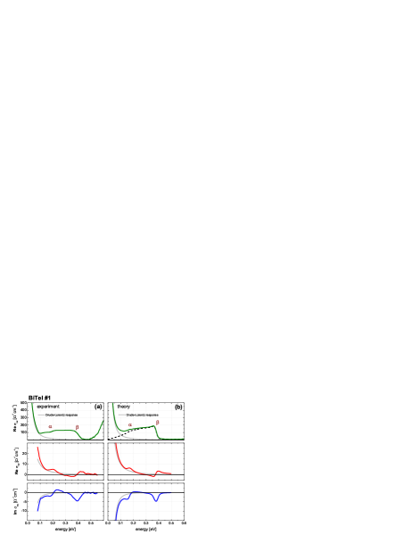
The experimental spectra for the -plane of sample #1 (with well above the Dirac point) are plotted in Fig. 2. Our theoretical results, also shown in Fig. 2, closely reproduce the experimentally observed spectra both in magnitude and energy position, including as well as the real and imaginary parts of . Two distinct features in the MO response are discerned in the spectra around 0.2 eV and 0.4 eV, in addition to a Drude-Lorentz response dominating the region below 0.1 eV. These two resonance structures well correspond to the intraband transitions and (see Fig. 1(a)) assigned in the spectra bitei_sigmaxx . The observed MO response (up to 5 cm-1 at 0.1-0.5 eV) at T is remarkably large for such a non-magnetic system. For a comparison, the interband contribution to the transverse conductivity for typical nonmagnetic semiconductors InSb, InAs, Ge, or GaAs at T is of the order of 0.01-0.3 cm-1 as calculated from the Faraday rotation faraday_theory . Even in the case of the ferromagnetic (Gd0.95Ca0.05)2Mo2O7, the MO signal in the 0.1-1 eV energy range governed by the Mo intraband transitions is an order of magnitude smaller, and only the spin chirality induced contribution present in Nd2Mo2O7 is comparable with the present system nmo . The observed MO activity at 3 T can well compare with the typical magnitude of the MO response () coming from the charge-transfer excitations in oxide ferromagnets nmo ; sro . In BiTeI, because of RSS of BCBs and TVBs, the optical transitions between the Rashba-split bands are allowed. Since these transitions have different dipole matrix elements for left and right circularly polarized light under applied magnetic field, a magneto-optical response results which scales linearly with the strength of SOI oppeneer . Hence, the large magneto-optical response of BiTeI is a direct consequence of the gigantic bulk RSS in this material. This is an astonishing effect of the SOI, since the magnetization of BiTeI at T is merely of the order of 10-4 /Bi bitei_chi , several orders of magnitude smaller than the spontaneous magnetization in the ferromagnets mentioned above.

To have a better insight into the consequences of RSS on the MO properties, the contribution of free carrier excitations has been subtracted by assuming a simple Drude model expressed with use of the cyclotron frequency , and the relaxation time . The dc conductivity was determined from the transport experiments, then , the only free parameter, was chosen so as to fit the low energy part of the experimental diagonal conductivity spectra. The Drude-Lorentz curves are also depicted in Fig. 2. Figure 3 shows the resulting spectra of and , whose Drude-Lorentz components are subtracted with the similar analysis, for all the samples investigated. The values of the effective mass () and the damping constant obtained from these fits are in good agreement with those found by the ARPES measurement bitei_arpes as well as those used for the aforementioned theoretical model.
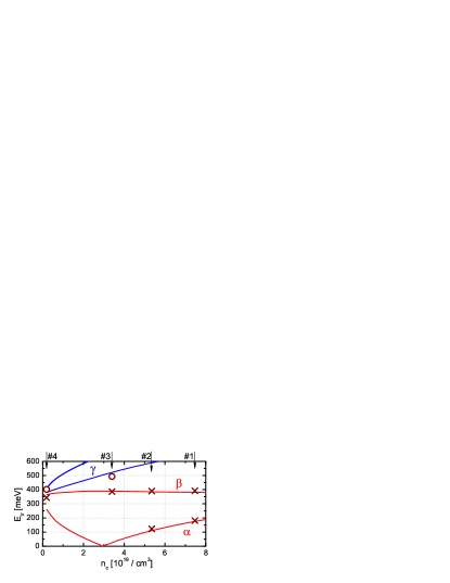
Next, we explain the evolution of different spectral features found in the MO response with varying carrier densities. Starting with sample #1, in the spectra one can identify the characteristic features of the intraband transitions as found previously bitei_sigmaxx , namely the vertical transitions to (from) the as depicted by () in Fig. 1(a). In external magnetic fields the Zeeman splitting is small compared to RSS, nevertheless the matrix elements of the intraband transitions become different for left and right circularly polarized lights. The dispersive-like features found in the real part of are the consequence of these processes, giving a clear evidence for the strong SOI in BiTeI. Lowering the Fermi level () to the level of sample #2 the band shifts toward lower energy with decreasing the magnitude, while the band remains at almost the same position. Further variation of (as in samples #3 and #4) causes slight shifts of as well, while is no more discernable in the measured frequency range. On the other hand, the spectral feature characteristic of the interband transitions (see Fig. 1(a)) enters into the detectable window from higher energies for samples #3 and #4, observed as a sharp rise in at the edge of the interband transition and as a dispersive spectral shape in the spectra. Figure 4 shows the calculated (solid lines) and observed (symbols) results for the relevant transition energies as a function of carrier density . The agreement between the experimental results and the theoretical predictions is excellent in the case of and transitions (that are assigned to the intraband excitations), and reasonably good in the case of the (interband) transitions.
To summarize, we have studied the magneto-optical response of BiTeI with a large Rashba spin splitting by systematically changing the position of the Fermi level around the band-crossing (Dirac) point. Given that BiTeI is a non-magnetic system, the observed MO response arising from the intraband transitions is found to be huge compared with conventional (spin degenerate) semiconductors. A theoretical model based on the calculated band structure has been constructed, which can quantitatively account for the experimental results, and also predict the significant impact of the Dirac point on the dc Hall effect.
This research is supported by MEXT Grand-in-Aid No.20740167, 19048008, 19048015, and 21244053, Strategic International Cooperative Program (Joint Research Type) from Japan Science and Technology Agency, by the Japan Society for the Promotion of Science (JSPS) through its “Funding Program for World-Leading Innovative R&D on Science and Technology (FIRST Program)”, the DFG research unit FOR 723, as well as by Hungarian Research Funds OTKA PD75615, CNK80991, Bolyai 00256/08/11, and TAMOP-4.2.1/B-09/1/KMR-2010-0002. G. A. H. S. acknowledges support from MEXT and DAAD.
References
- (1) D. Awschalom and N. Samarth, Physics 2, 50 (2009).
- (2) S. D. Bader and S. S. P. Parkin, Annu. Rev. Cond. Matter Phys. 1, 71 (2010).
- (3) J. Sinova and I. Žutić, Nat. Mater. 11, 368 (2012).
- (4) R. Winkler, Springer Tracts in Modern Physics 191 (Springer, Berlin, 2003).
- (5) S. Murakami, N. Nagaosa, and S. C. Zhang, Science 301, 1348 (2003).
- (6) S. N. Ganichev et al., Nature 417, 153 (2002).
- (7) K. H. Bennemann, J. Mag. Mag. Mater. 200, 679 (1999).
- (8) K. Ishizaka et al., Nat. Mater. 10, 521 (2011).
- (9) M. S. Bahramy, R. Arita, and N. Nagaosa, Phys. Rev. B 84, 041202(R) (2011).
- (10) M. S. Bahramy, B.-J. Yang, R. Arita, and N. Nagaosa, Nat. Commun. 3, 679 (2012).
- (11) J. S. Lee et al., Phys. Rev. Lett. 107, 117401 (2011).
- (12) S.-Q. Shen, M. Ma, X. C. Xie, F. C. Zhang, Phys. Rev. Lett. 92, 256603 (2004).
- (13) A. A. Burkov and L. Balents, Phys. Rev. B 69, 245312 (2004).
- (14) W. Xu, C. H. Yang, and J. Zhang, Appl. Phys. Lett. 91, 221911 (2007).
- (15) M. S. Kushwaha, Phys. Rev. B 74, 045304 (2006).
- (16) K. Sato, Japan. J. Appl. Phys. 20, 2403 (1981).
- (17) H. Fukuyama, Prog. Theor. Phys. 42, 1284 (1969).
- (18) Details of ab-inito calculations can be found in Ref. bitei_theory .
- (19) G. D. Mahan, Many-Particle Physics, 3rd edition (Plenum, New York, 2000).
- (20) L. M. Roth, Phys. Rev. 133, A542 (1964).
- (21) I. Kézsmárki et al., Phys. Rev. B 72, 094427 (2005).
- (22) Z. Fang et al., Science 302, 92 (2003).
- (23) P. M. Oppeneer, T. Maurer, J. Sticht, and J. Kübler, Phys. Rev. B 45, 10924 (1992).
- (24) G. Schober et al., cond-mat/1111.5800, Phys. Rev. Lett. (in press).