Measuring roughness of buried interfaces by sputter depth profiling
Abstract
In this communication, we report results of a high resolution sputter depth profiling analysis of a stack of 16 alternating MgO and ZnO nanolayers grown by atomic layer deposition (ALD) with thickness of 5.5 nm per layer. We used an improved dual beam approach featuring a low energy normally incident direct current sputtering/milling ion beam (first beam). Intensities of 24Mg+ and 64Zn+ secondary ions generated by a pulsed analysis ion beam (second beam) were measured as a function of sample depth by time-of-flight secondary ion mass spectrometry (TOF SIMS).
Experimental results of this dual beam TOF SIMS depth profiling processed in the framework of the mixing-roughness-information (MRI) model formalism demonstrate that such an approach is capable of providing structural information for layers just a few nm thick. Namely, it was established that the interfacial roughness of the MgO/ZnO multilayer structure equals 1.5 nm. This finding by TOF SIMS was cross-validated by independent measurements with specular X-ray reflectivity (XRR) technique. In addition, the TOF SIMS-MRI analysis suggests that the obtained 1.5 nm roughness should be attributed to the native roughness (jagged type) of the interface rather than to interdiffusion at the interface during the ALD synthesis.
pacs:
68.35.bg, 68.35.Ct, 81.15.Gh, 82.80.Ms, 82.80.RtI Introduction
Quality of interfaces in multilayered materials is of great interest and importance, since the way layers adhere to each other greatly affects their performance: spin-based electronics,1 giant magnetoresistance structures/devices,2 high- multilayer materials,3 artificial Bragg crystals,4 heat transfer in nanostructures,5 and others.
A powerful and efficient set of methods commonly used to determine (i) single layer thickness, (ii) roughness and (iii) density in a multilayer system combines the X-ray reflectivity (XRR) method with ellipsometry. XRR technique uses the values of (i), (ii), and (iii) as fitting parameters jointly with some type of boundary conditions to solve a general inverse problem of wave scattering.6 ; 7 XRR results can be partially validated by optical ellipsometry, which is also based on solving a similar inverse problem. It relies on refractive index (a function of density) and a layer thickness in a single/multiple layered structure, and depends on boundary conditions as well. This makes the data fitting model sensitive and dependent on many free parameters, which can grow fast when the number of layers in the layered structure increases. Moreover, such indirect techniques based on measuring optical responses of a material may become inefficient if one needs to work with three-layer stacks (or even more general case of layers) where repetition of certain layers in an -layer stack varies, as, for instance, occurs in the case of metamaterials.8 ; 9 A problem will also exist for multilayer semiconductor heterostructures, where the composition variation between nearest layers is about the same with a few percent difference in solid solution content.10 Hence, the change in density is so small that the sensitivity of the XRR method may be insufficient for characterization of such materials. Thus, the search for a more direct and established approach to characterization of nm-thick layers in a variety of multilayered structures, which is sensitive and independent on optical properties, is highly desirable. It can complement XRR and ellipsometry techniques, and in some cases might do the job, which is beyond their capabilities.
Mass spectrometry retains its importance in basic physics,11 chemistry,12 and in materials science13 due to a number of unique advantages, such as sensitivity to isotopic ratio, trace amounts of elemental/molecular species on the surface and in the bulk, etc. In this context, an extension of its capabilities is of great interest. In the present paper, we demonstrate that properly designed mass spectrometry of secondary ion species in sputter depth profiling experiments can successfully reveal structural features of nanolayered structures and characterize their surface and interfaces. To this end, an improved dual beam secondary ion mass spectrometry (SIMS) with low energy normal incidence sputtering/milling was applied to depth profile a layered MgO/ZnO8 structure grown by atomic layer deposition. The obtained depth profiles were processed in terms of mixing-roughness-information (MRI) model. This model has analytical solutions with, in case of SIMS, two variable parameters having straightforward physical interpretation: the ion beam mixing length and the roughness. The SIMS-MRI results are compared to structural parameters obtained by specular XRR measurements to confirm the correctness of made conclusions.
II Samples and Experimental
A layered structure 5.5-nm MgO/5.5-nm ZnO8 was grown by ALD on a Si substrate using established precursor chemistries for MgO14 and ZnO15 ; 16 and characterized by X-ray diffraction and ellipsometry. The structural data obtained from these measurements indicated that MgO layers are amorphous and ZnO layers are polycrystalline in the wurtzite phase. The roughness of the Si substrate was 0.3 nm. The initial layer-to-layer mixing due to thermal diffusion during growth at =473 K is expected to be extremely low. Specular X-ray reflectivity measurements were made with a Philips X’Pert Pro MRD diffractometer using Cu K radiation (=1.5418 ) and operated at 30 kV/40 mA. The incident X-ray beam was conditioned by a 60 mm graded parabolic W/Si mirror with a 0.8∘ acceptance angle and a 1/32∘ divergence slit. The reflected beam was collected with a PW3011/20 sealed proportional point detector positioned behind a 0.27∘ parallel plate collimator.
Secondary ion mass spectrometry studies were performed in a
custom-designed SARISA (Surface Analysis by Resonance Ionization
of Sputtered Atoms) instrument in the Materials Science Division
at Argonne National Laboratory.17 SARISA combines two
independently optimized Ar+ ion beams: one of low energy (a few
hundred eV) and normal incidence for ultimate depth resolution ion
milling/sputtering, and another for elemental time-of-flight (TOF)
SIMS analysis with high lateral resolution. This arrangement is
based on the known powerful dual beam approach to depth
profiling18 and can be dubbed
gentleDB00footnotemark: 0.00footnotetext:
gentle
stands for low energy normal incidence sputtering, lenis,
which is gentle/soft in Latin There are three main
advantages of this setup. First, depth resolution is controlled by
the milling beam if the parameter is much smaller than
unity, or (see below). Second and third, normal
incidence permits varying the impact energy of primary ions by
target bias and does not introduce additional roughening of a
sample surface.19 ; 20
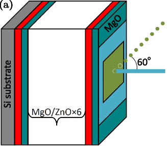
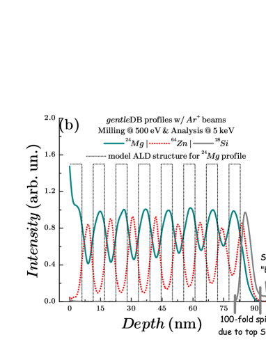
Elemental depth profiles, concentration/intensity versus depth, of the sandwich structure were obtained by a sequence of alternating cycles. Ion milling by a raster scanned primary direct current Ar+ ion beam at 500 eV and normal incidence17 is followed by TOF SIMS analysis of revealed subsurface (various depths, from surface down to substrate) by a raster scanned pulsed (200 ns long) Ar+ ion beam at 5 keV energy and 60∘ incidence with respect to the target normal, as shown schematically in Fig.1a. This pair of cycles is repeated multiple times until the Si substrate is reached, which is monitored by Si+ peak intensity in a mass spectrum. In the depth profile, the Si substrate grows in as a spike attributed to 100-fold enhanced secondary ion yield due to presence of SiO2. It then stabilizes at a lower constant level, as shown in Fig.1b. The depth resolution is controlled ultimately by the milling beam characteristics. This condition is fulfilled if the parameter called effective erosion efficiency specific for the milling beam is much higher than that of the analytical beam, or . Here, is a sputtering yield, which depends on a beam energy , the primary projectile species and an angle they attack the surface, is the current density, is the total sputtering time during which an ion beam is on. In our experimental setup was 10-5.
The milling beam was digitally raster scanned over a square area of 1 mm2 (blue square in Fig.1a), while the analytical beam was raster scanned over a square of 500500 m2 (green square in Fig.1a). Both raster areas were precisely overlapped by using an in situ Schwarzschild microscope,17 and ex situ by white light profilometry.21
Ion beam currents were measured and focused in situ by a custom made graphite Faraday cup (FC) consisting of an internal pin and inlet holes of 250 m dia. on the mask. Such a FC design permits to control focusing conditions of an ion beam. Ion beam profiles were checked and known to have a symmetric Gaussian distribution by burning dents in soft materials and profiling the dents by ex situ white light profilometry.21 It allows one to precisely calculate a current density of an ion beam using a known dc current value measured on the FC. The milling beam parameters at 500 eV were 1 A dc and a FWHM of Gaussian-like beam profile of 150 m. The analytical beam characteristics at 5 keV were 300 nA dc and a FWHM of Gaussian-like beam profile of 40 m, and then reduced down to 30nA by choosing an appropriate aperture.
The measured energy spread of our low energy column17 is 23 eV yielding at 500 eV milling energy. Thus, the milling beam can be considered as monoenergetic with high precision.
III Results, Discussion and Conclusions
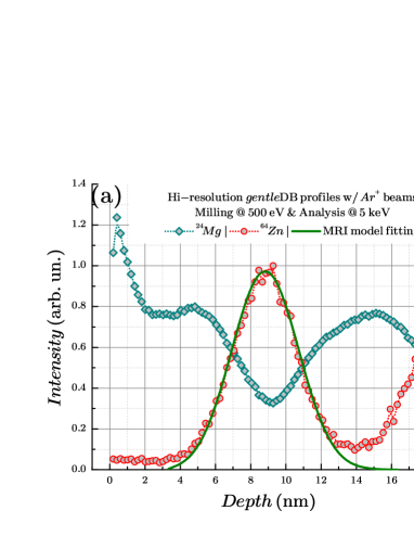
Fig.1b demonstrates SIMS depth profiles of Mg+ and Zn+ obtained by gentleDB at 500 eV ion milling, reflecting the full set of peaks in the periodical structure, 8 peaks for MgO and ZnO each. Fig.2a is a high-resolution profile obtained under the same conditions as the profiles in Fig.1b, but at small ion milling increments, so that the depth difference between two consecutive points is 0.2 nm, corresponding to monolayer thickness for wurtzite ZnO.
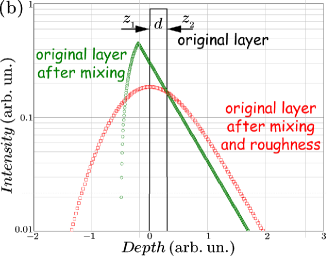
We used the high-resolution Zn+ depth profile for further evaluation of structure features of the multilayer ALD stack. This was accomplished in the terms of an analytical approach called mixing-roughness-information (MRI) model.22 ; 23 In essence, the model has 3 physically meaningful parameters. Mixing is characterized by the ion beam mixing length , a scale at which two perfect layers of different compositions with perfect abrupt interface experience mutually uniform interpenetration under nonreactive gas bombardment. Roughness is the root-mean-square (rms) roughness . By the term ”information”, the depth of collecting information is meant, which is the same as the escape depth commonly used in surface analysis techniques. In general, is a variable parameter, but in the case of SIMS it can be fixed at a value of 1-2 monolayers.24 The effects of the two main processes, mixing and roughness, on the resulting peak depth profile are shown in Fig.2b. It is seen that, in the case of an ideal rectangular layer, the ion beam induced mixing leads to asymmetric depth profile, which may get additional broadening and symmetrization due to the rms roughness, depending on the interplay between and values. The effect of the information depth is not incorporated, since it is expected to be negligible.
The green solid curve in Fig.2a superimposed on the Zn+ depth profile is the best fit of the experimental curve by the MRI model. The fit parameters were as follows: is 0.4 nm and is 1.5 nm, while was fixed at 0.2 nm, corresponding to the wurtzite ZnO monolayer thickness. The flat thickness of the layer , which is a thickness of an ideal flat layer (see Fig.2b) defining boundary conditions for the model, appeared to be 3 nm yielding the total single ALD layer thickness to be of 6 nm. The sharpness of the last interface between the Si substrate and the ZnO layer can also be estimated. An up-slope of the Si signal shown in Fig.1b results in a roughness of 0.4 nm.
To cross-validate the results obtained by MRI modeling of the experimental data, we performed specular XRR measurements on a MgO/ZnO sample prepared under identical conditions. The use of XRR in this case seems to be a valid approach, since its sensitivity to fluctuations of the thickness (that can range in characteristic length scale) at the wavelength of 1.5 can be anticipated to be similar to that of SIMS based on a single ion penetration in the fine interfacial structure. Fig.3 represents a typical specular XRR profile obtained for the MgO/ZnO8 sandwich. Fitting of experimental data was performed with a commercial software package (Panalytical X’Pert Reflectivity) which makes use of the Parratt recursion formalism for reflectivity.25 Due to the relatively large number of discreet layers present in the MgO/ZnO8 heterostructure, several periodic constraints were applied to reduce the set of fitting parameters which would otherwise be required. A simple ideally periodic model assuming identical ZnO/MgO bilayers failed to reasonably approximate the data. A second model where the first ZnO layer and last MgO layer were treated discreetly as described by Jensen et al7 also failed to produce adequate fits to the experimental data. However, simulations where the density, , thickness, and roughness, , of each subsequent ZnO and MgO layer were constrained to increase linearly with increasing distance from the substrate provided a good match to the experimental reflectivity curve. The experimental fit was further optimized by allowing each , thickness, and to vary from the linear model within reasonable physical constraints (e.g. bulk density values). The resulting reflectivity fits confirmed the parameters values extracted from SIMS data: the average thicknesses of ZnO and MgO appeared to be 6.4 nm and 6.1 nm, with average roughness values of 1.10.2 nm and 1.60.3 nm, respectively. Parameters of the SiO2 layer on the top of the Si substrate were also of the expected values: thickness of 1.2 nm, =0.3 nm.

Thus, XRR data independently proves that SIMS analysis along with the chemical information is capable of revealing detailed internal interface structure, when distortions/artifacts related to a profiling procedure are minimized to a scale, much smaller than that of a feature to be investigated. In the case of gentleDB approach, this means that the extracted mixing parameter =0.4 nm is of the same order as the inherent escape depth of a secondary ion, a physical limitation of the technique. Therefore, the found 1.5 nm interfacial roughness of the MgO/ZnO layers is due to an ultra-short ion beam mixing length/lattice disturbance in gentleDB profiling procedure. XRR also proves that the obtained 1.5 nm roughness is reasonable and falls well within the range provided by other experimental methods, both in this study and other studies of layered laminate oxides performed by AFM/STM,26 XRR3 ; 7 and TEM.3
Let us extend the finding by gentleDB SIMS in conjunction with MRI results. First of all, in the context of the advantages of the low energy orthogonal sputtering described above, the rms roughness is believed to be a native interface roughness of the grown ALD structure. In addition, it is known that XRR cannot distinguish between the interfacial roughness and the interdiffusion.7 One may assume that the interdiffusion at the interface is a process similar in some way to the ion beam mixing, which normally causes a mutually uniform layers interpenetration,23 thus blurring the initially sharp interfaces and forming a mixed-up interlayer. If the interdiffusion is pronounced, the MRI model suggests that the gentleDB SIMS depth profiles (keeping in mind the limit of going down to zero) would look more asymmetric, closer to the green curve shown in Fig.2b. For this particular MgO/ZnO structure grown at only 473 K, the shapes of the Mg+ and Zn+ peaks, which are broad and nearly symmetric, in measured depth profiles suggest that the estimated 1.5 nm roughness corresponds to native roughness (i.e., ”jagged” junction), rather than to interdiffusion, or that the interdiffusion does not exceed 0.4 nm from the total 1.5 nm.
To summarize, gentleDB SIMS, in conjunction with the MRI model, is a direct, but destructive and relatively slow method, which does not require prior assumptions regarding the sample. On the contrary, the specular XRR is indirect, but nondestructive and relatively fast method, which is model dependent and needs prior information about the sample. Thus, when both techniques are applied to characterize buried interfaces in nanolayered materials, they complement and enhance each other, and yield comprehensive physical/structural and chemical information on the material: interfacial roughness distinguishing interdiffusion from native/jagged roughness, thickness, density, as well as elemental depth profiles, including trace impurities, redistribution of isotopes in isotopically modulated structures,27 and many other possible applications.
IV Acknowledgments
This work was supported under Contract No. DE-AC02-06CH11357 between UChicago Argonne, LLC and the U.S. Department of Energy.
References
- (1) S. Dash, S. Sharma, J. Le Breton, J. Peiro, H. Jaffrés, J.M. George, A. Lemaître and R. Jansen, Phys. Rev. B 84, 054410 (2011).
- (2) I. Bakonyi and L. Péter, Progress in Materials Science 55, 107 (2010).
- (3) M. de Pauli, A. Malachias, H. Westfahl, J. Bettini, A. Ramirez, G. S. Huang, Y.F. Mei and O.G. Schmidt, J. Appl. Phys. 109, 063524 (2011).
- (4) A. Biswas and D. Bhattacharyya, J. Appl. Phys. 109, 084311 (2011).
- (5) P. Hopkins, J. Duda, C. Petz and J. Floro, Phys. Rev. B 84, 035438 (2011).
- (6) G.A. Valkovskiy, M.V. Baidakova, P.N. Brunkov, S.G. Konnikov, M.A. Yagovkina and J.M. Zadiranov, Phys. Status Solidi A 208, 2623 (2011).
- (7) J.M. Jensen, A.B. Oelkers, R. Toivola, D.C. Johnson, J.W. Elam and S.M. George, Chem. Mater. 14, 2276 (2002).
- (8) J.D. Baena, L. Jelinek and R. Marqués, New Journal of Physics 7, 166 (2005).
- (9) J.A. Monsoriu, R.A. Depine, M.L. Martínez-Ricci, E. Silvestre and P. Andrés, Optics Letters 34, 3172 (2009).
- (10) D. Chiba, N. Akiba, F. Matsukura, Y. Ohno and H. Ohno, Appl. Phys. Lett. 77, 1873 (2000).
- (11) K.D. McKeegan, A.P.A. Kallio, V.S. Heber, G. Jarzebinski, P.H. Mao, C.D. Coath, T. Kunihiro, R.C. Wiens, J.E. Nordholt, R.W. Moses, D.B. Reisenfeld, A.J.G. Jurewicz and D.S. Burnett, Science 332, 1528 (2011).
- (12) M. Mrksich, ACS Nano 2, 7 (2008).
- (13) J.C. Vickerman and I.S. Gilmore, Surface analysis: the principal techniques (2nd ed., Wiley, Chichester, UK, 2009).
- (14) M. Putkonen, T. Sajavaara and L. Niinistö, J. Mater. Chem. 10, 1857 (2000).
- (15) V. Lujala, J. Skarp, M. Tammenmaa and T. Suntola, Appl. Surf. Sci. 82-83, 34 (1994).
- (16) J.W. Elam, Z.A. Sechrist and S.M. George, Thin Solid Films 414, 43 (2002).
- (17) I.V. Veryovkin, C.E. Tripa and M.J. Pellin, Physics Procedia 1, 379 (2008).
- (18) K. Iltgen, C. Bendel, A. Benninghoven and E. Niehuis, J. Vac. Sci. Technol. A 15, 460 (1997).
- (19) T.J. Ormsby, D.P. Chu, M.G. Dowsett, G.A. Cooke and S.B. Patel, Appl. Surf. Sci. 144-145, 292 (1999).
- (20) AFM measurements of bottoms of sputtered craters under the same conditions described here, to be published.
- (21) S.V. Baryshev, A.V. Zinovev, C.E. Tripa, R.A. Erck and I.V. Veryovkin, Appl. Surf. Sci. 258, 6963 (2012).
- (22) S. Hofmann, J. Vac. Sci. Technol. B 10, 316 (1992).
- (23) S. Hofmann, Rep. Prog. Phys. 61, 827 (1998).
- (24) G. Betz and G.K. Wehner, Topics in Applied Physics 52, 11 (1983).
- (25) L. Parratt, Phys. Rev. 95, 359 (1954).
- (26) T. Asikainen, M. Ritala, M. Leskelä, T. Prohaska, G. Friedbacher and M. Grasserbauer, Appl. Surf. Sci. 99, 91 (1996).
- (27) C.W. Schneider, M. Esposito, I. Marozau, K. Conder, M. Doebeli, Y. Hu, M. Mallepell, A. Wokaun and T. Lippert, Appl. Phys. Lett. 97, 192107 (2010).