Spin transport and spin dephasing in zinc oxide
Abstract
The wide bandgap semiconductor ZnO is interesting for spintronic applications because of its small spin-orbit coupling implying a large spin coherence length. Utilizing vertical spin valve devices with ferromagnetic electrodes (TiN/Co/ZnO/Ni/Au), we study the spin-polarized transport across ZnO in all-electrical experiments. The measured magnetoresistance agrees well with the prediction of a two spin channel model with spin-dependent interface resistance. Fitting the data yields spin diffusion lengths of 10.8 nm (2 K), 10.7 nm (10 K), and 6.2 nm (200 K) in ZnO, corresponding to spin lifetimes of 2.6 ns (2 K), 2.0 ns (10 K), and 31 ps (200 K).
The successful injection, transport, manipulation, and detection of spin-polarized currents in semiconductors is a prerequisite for semiconductor spintronics.Prinz (1998) In this context, the spin dephasing time of mobile charge carriers – and the associated length scale for coherent spin transport – are fundamental parameters. The wide bandgap II-VI semiconductor zinc oxide has a small spin-orbit coupling Fu and Wu (2008) implying a large spin coherence length. This makes ZnO interesting for (opto)electronics or spin-based quantum information processing. While other semiconductors like GaAs and related III-V compounds have been studied extensively,Awschalom and Samarth (2002) only few reports on spin-coherent properties in ZnO exist.Ghosh et al. (2005); Liu et al. (2007); Janßen et al. (2008) Using time-resolved Faraday rotation (TRFR), electron spin coherence up to room temperature in epitaxial ZnO thin films was first observed by Ghosh et al. with a spin dephasing time of ns at 10 K.Ghosh et al. (2005) Our ZnO thin films display ns (also at 10 K) in similar optical experiments.Weier (2010); Opel (2012) Reports on electrical spin injection, however, are rareChen et al. (2002); Ji et al. (2009); Shimazawa et al. (2010) and mainly focus on technical aspects rather than fundamental spin-dependent properties of ZnO. The highest reported values for the magnetoresistance (MR) in ZnO-based spin valve structures are 1.38% and 1.12% (90 K) for thicknesses of the ZnO layer of 3 nm and 10 nm, respectively.Ji et al. (2009) Here, we investigate the transport and the dephasing of spin-polarized charge carriers in ZnO utilizing all-electrical, vertical spin valve devices with ferromagnetic (FM) electrodes. We do not focus on the mechanism of spin injection and the general problem of overcoming the conductance mismatchSchmidt et al. (2000) between ZnO and the ferromagnetic layers in the spin valve structure. The experimental observation of a large MRBaibich et al. (1988); Binasch et al. (1989); Gijs and Bauer (1997) of up to 8.4% in our FM/ZnO/FM junctions demonstrates the successful transport of a spin-polarized ensemble of electrons across several nanometers in ZnO.
The thin film multilayer heterostructures (left inset in Fig. 1) were fabricated on (0001)-oriented, single crystalline Al2O3 substrates via laser-MBE in combination with electron-beam physical vapor deposition (EBPVD) in an ultra-high vacuum cluster system.Gross et al. (2000) Laser-MBE was carried out by pulsed laser deposition (PLD) from stoichiometric polycrystalline targets, using a KrF excimer laser with a wavelength of 248 nm at a repetition rate of 10 Hz.Opel (2012) EBPVD was performed in high vacuum ( mbar) at room temperature. The multilayer stack consists of (i) a 12 nm thin TiN film as a non-ferromagnetic, metallic bottom electrode, deposited via PLD at C in Ar atmosphere of mbar with a laser fluence of 2 J/cm2; (ii) a 11 nm thin Co film (EBPVD) as the first ferromagnetic electrode; (iii) a semiconducting ZnO film (PLD, C, Ar, mbar, 1 J/cm2) with thickness systematically varied in the range from 5 nm to 100 nm in a series of samples; (iv) a 11 nm thin Ni film (EBPVD) as the second ferromagnetic electrode; and finally (v) a 24 nm thin Au film (EBPVD) as a capping layer and top electrode.
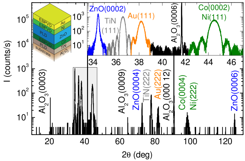
The structural quality of the multilayer stack was investigated by high-resolution X-ray diffractometry in a four circle diffractometer using Cu K radiation. The out-of-plane --scan does not reveal any secondary phases (Fig. 1). All detected reflections can be assigned to the respective materials of the spin valve multilayer structure. The cubic materials TiN, Ni, and Au grow (111)-oriented, the hexagonal Co and ZnO layers (0001)-oriented. The signals from Co and Ni cannot be separated as the lattice parameter of hcp Co ( nm)Martienssen and Warlimont (2005) is twice as large as the lattice spacing nm of the -planes in cubic Ni with nm.Martienssen and Warlimont (2005) For the TiN, Co, and Au layers, the --scan shows satellites due to Laue oscillations (right inset of Fig. 1) demonstrating coherent growth with small interface roughness and indicating a high structural quality. From the out-of-plane reflections, we calculate the corresponding lattice parameters for each layer ( nm, nm, nm, nm, nm) and find them very close () to the respective bulk values.Martienssen and Warlimont (2005) The high structural quality is also confirmed by the narrow full widths at half maximum (FWHM) of the rocking curves (not shown here) for the respective out-of-plane reflections. We obtain for TiN(111), for Co(0002), for ZnO(0002), and for Au(111), demonstrating a low mosaic spread. -scans around asymmetric reflections (not shown here) exhibit a sixfold in-plane symmetry for all layers with clear epitaxial relationships: Al2O TiN Co ZnO Ni Au. From this detailed structural analysis, it becomes evident that each layer is aligned with respect to the oxygen sublattice of the (0001)-oriented Al2O3 substrate. This effect has already been reported for TiN(111),Talyansky et al. (1999) Co(0001),Ago et al. (2010) ZnO(0001),Chen et al. (1998) and Au(111).Kästle et al. (2002) Our results prove that the respective in-plane orientations of the single layers are preserved with excellent quality when grown on top of each other.
The magnetic properties of the multilayer stack were studied via superconducting quantum interference device (SQUID) magnetometry at temperatures between 2 K and 300 K in magnetic fields of T applied in-plane. At all investigated temperatures, the magnetization shows a ferromagnetic hysteresis for low fields. The shape of represents a superposition of two distinct hysteresis curves with different coercive fields (Fig. 2(a)). We assign the larger to the Ni film and the lower to the Co layer, as confirmed by investigating a modified structure without Ni (not shown here). From these coercivities, the magnetizations of Ni and Co (red horizontal arrows in Fig. 2) are expected to be aligned parallel for and antiparallel (shaded regions in Fig. 2) for for the field up-sweep direction or for the sweep-down direction, respectively. This independent switching of the magnetizations is a key requirement for the successful realization of a spin valve device.
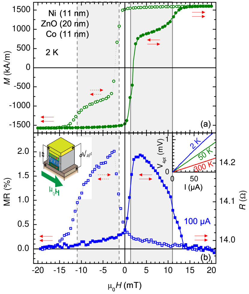
Using photolithography, Ar ion beam milling and lift-off processes, the multilayer stack was patterned into vertical mesa structures with junction areas of m2. These spin valve junctions were investigated by magnetotransport at temperatures between 2 K and 300 K in a liquid He magnet cryostat system with the magnetic field again applied in-plane. The vertical transport was studied in standard four-point geometry by applying a constant dc bias current and measuring the voltage drop across the spin valve junction (left inset of Fig. 2(b)). The --characteristics of all investigated samples display a linear regime for small bias currents of A (right inset in Fig. 2(b)).111The linear behavior is expected in the tunneling regime. For higher currents, heating leads to non-linear --characteristics. In the following and for the evaluation of the magnetoresistance (MR) of samples with different thicknesses of the ZnO layer below, we restrict to this Ohmic regime for all investigated temperatures.
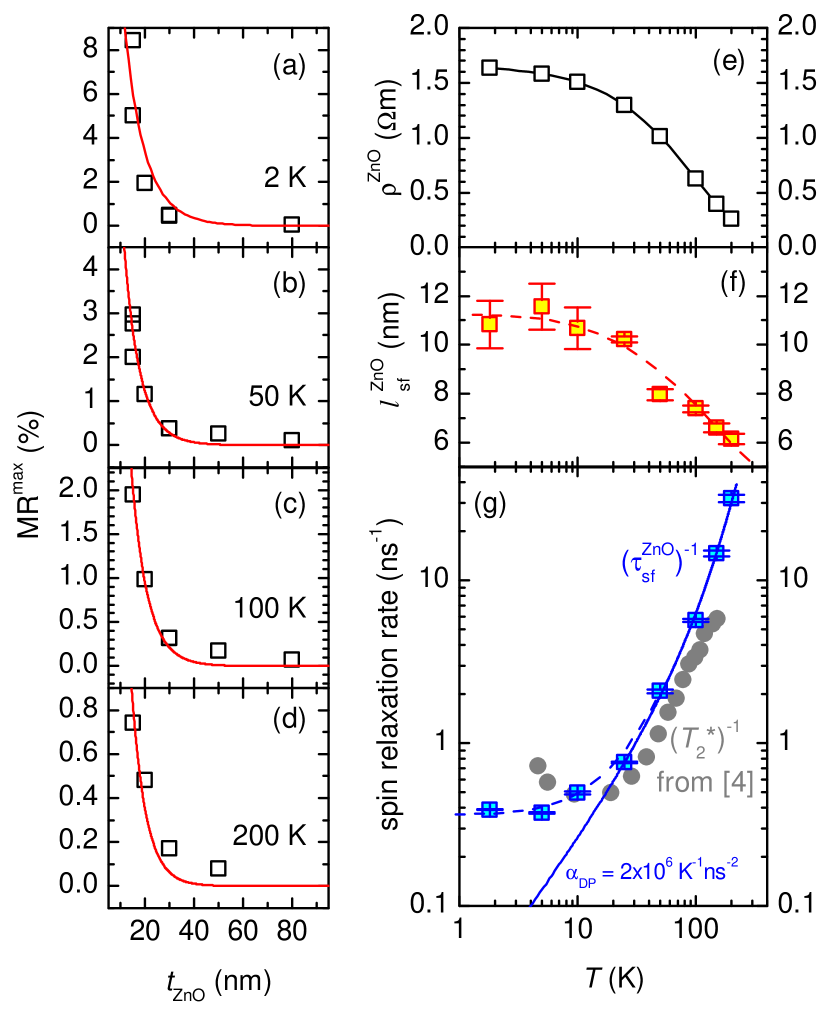
The resistance is found to scale with , demonstrating that it is not dominated by the ferromagnetic layers. The resistivity determined by multiplying with the junction area and dividing by the respective thickness of the whole multilayer stack shows the same temperature dependence for all spin valve junctions as for a reference junction of TiN/ZnO/Au without ferromagnetic electrodes. increases by about one order of magnitude from 300 K to 2 K (Fig. 3(e)). From the analysis of the Hall effect of our ZnO thin films deposited directly on Al2O3 substrates, we obtained a high and almost constant carrier concentration of over the whole temperature range (not shown here). Assuming an effective mass of , from this value we estimate a Fermi temperature of K. With from Fig. 3(e), we further find a low carrier mobility of .
When sweeping the magnetic field, shows a hysteresis between the field up-sweep and down-sweep directions with two resistive states (Fig. 2(b)), corresponding very well to the hysteresis discussed above. For magnetic fields with an antiparallel magnetization configuration of the Ni and Co electrodes (shaded regions in Fig. 2), is significantly higher than for the parallel configurations. This is evidence that our vertical mesa structures act as spin valve devices.222This statement is further confirmed by angle-resolved measurements, see supplemental material. For nm and at 2 K, the magnetoresistance
| (1) |
reaches a maximum value MRmax of almost 2% (Fig. 2(b)). MR is independent of the potential difference across the spin valve for dc bias currents up to A. Evaluating MR from different samples with different thicknesses nm of the semiconducting ZnO layer, we find that MRmax sensitively depends on . At 2 K, MRmax rapidly decreases from 8.4% for 15 nm to 0.06% for 80 nm (Fig. 3(a)). The same behavior is observed at higher temperatures of 50 K, 100 K, and 200 K with the overall values becoming significantly smaller (Fig. 3(b-d)).
Following the Valet-Fert approach,Valet and Fert (1993); Fert and Jaffrès (2001) we fit MRmax to a two spin channel model with spin-dependent conductivities to extract the spin diffusion length for ZnO. We use the same nomenclature as in Ref. Fert and Jaffrès, 2001. As material parameters we plug in the resistivities nm and nm,Martienssen and Warlimont (2005) the spin asymmetry coefficients (Ref. Moreau et al., 2007) and (Ref. Bass and Pratt, 1999), as well as the spin diffusion lengths nm (Ref. Moreau et al., 2007) and nm (Ref. Piraux et al., 1998) for Ni and Co, respectively. Since these parameters have only small influence on the MR, we assume for simplicity that they are independent of temperature. The spin-dependent resistivities of Ni and Co are then given by .Fert and Jaffrès (2001) The only temperature-dependent input parameter for the fit process is which was determined independently from the TiN/ZnO/Au reference sample (Fig. 3(e)).
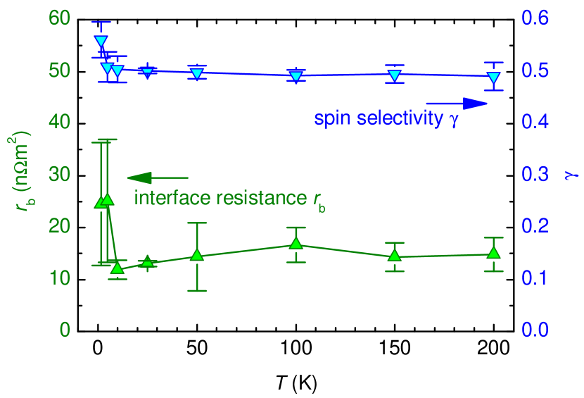
The fit curves after Eq. (31) of Ref. Fert and Jaffrès, 2001 clearly reproduce the measured MRmax, reflecting a fair agreement between model and experiment (red lines in Fig. 3(a-d)). From the fits, we extract and obtain a value of (10.81.0) nm for 2 K (Fig. 3(f)). For increasing temperature, stays first nearly constant with a value of (10.70.2) nm at 10 K. For higher temperature, it decreases to (6.20.2) nm at 200 K. We further extract the interface resistance and the spin selectivity , and find both values nearly independent of temperature (see supplemental material). For comparison, we calculate MRmax for nm and 10 nm at 90 K and obtain 12% and 3.7%, respectively, by far exceeding the previously reported values of 1.38% and 1.12%.Ji et al. (2009)
The spin diffusion length is determined by the transport mean free path and the spin-flip length .Fert and Jaffrès (2001); Bass and Pratt (2007) Here, is the spin lifetime and the mean free time between collisions. The latter can be derived from the measured resistivity by using the simple Drude relation . For the mean square velocity of the charge carriers we use , since we are moving from a degenerate Fermi to a classical gas on increasing the temperature. With and , we obtain
| (2) |
With the experimental values 510, K, and from Fig. 3(e), the spin relaxation rate can be derived. It decreases from (321.7) ns-1 at 200 K to (0.490.011) ns-1 at 10 K and further to (0.390.0021) ns-1 at 2 K (Fig. 3(g)). Evidently, this behavior obtained from our all-electrical detection scheme agrees well with the temperature dependence of derived from optical TRFR experiments in ZnO thin filmsGhosh et al. (2005) in an intermediate temperature range of (Fig. 3(g)). For lower temperatures, however, increases again while becomes constant below 10 K.
Two different spin relaxation mechanisms are considered as important in ZnO: the Dzyaloshinsky-Moriya (DM) mechanism due to an anisotropic exchange between localized electronic states and the D’yakonov-Perel’ (DP) mechanism due to the reflection asymmetry of the crystal lattice along the -axis.Harmon, Putikka, and Joynt (2009) For high temperatures ( K), the DP process becomes dominant.Harmon, Putikka, and Joynt (2009) Its temperature dependence is given byHarmon, Putikka, and Joynt (2009)
| (3) |
with the material-dependent efficiency . A fit after Eq. (3) reproduces our data very well for K (blue line in Fig. 3(g)). We note that the fit yields being four orders of magnitude larger than the theory value of calculated for bulk ZnO with low carrier concentration.Harmon, Putikka, and Joynt (2009) We attribute this discrepancy to the low carrier mobility of our ZnO thin films. For K, however, the DM mechanism is predicted to become dominant, resulting in a nearly -independent spin relaxation rate.Harmon, Putikka, and Joynt (2009) This behavior was not reported for optical TRFR experiments in ZnO thin films,Ghosh et al. (2005) but is indeed observed in our ZnO-based spin valves for temperatures down to 2 K (dashed line in Fig. 3(g)).
In summary, we create and detect a spin-polarized ensemble of electrons and demonstrate the transport of this spin information across several nanometers in ZnO. We determine the spin diffusion length and the spin lifetime in an all-electrical experiment and obtain large values of nm and ns at 2 K. The evolution of the measured spin relaxation rates with temperature is consistent with the D’yakonov-Perel’ mechanism for K. For future semiconductor spintronic devices, such all-electrical experiments will be mandatory to extract the relevant spin transport parameters.
Acknowledgements.
We thank A. Erb for the preparation of the polycrystalline PLD targets, T. Brenninger for technical support, and M. S. Brandt for stimulating discussions. This work was supported by the Deutsche Forschungsgemeinschaft via SPP 1285 (project no. GR 1132/14) and the German Excellence Initiative via the “Nanosystems Initiative Munich (NIM)”.References
- Prinz (1998) G. A. Prinz, Science 282, 1660 (1998).
- Fu and Wu (2008) J. Y. Fu and M. W. Wu, J. Appl. Phys. 104, 093712 (2008).
- Awschalom and Samarth (2002) D. D. Awschalom and N. Samarth, in Semiconductor Spintronics and Quantum Computation, edited by D. D. Awschalom, D. Loss, and N. Samarth (Springer, Berlin, 2002) pp. 147–193.
- Ghosh et al. (2005) S. Ghosh, V. Sih, W. H. Lau, D. D. Awschalom, S. Bae, S. Wang, S. Vaidya, and G. Chapline, Appl. Phys. Lett. 86, 232507 (2005).
- Liu et al. (2007) W. K. Liu, K. M. Whitaker, A. L. Smith, K. R. Kittilstved, B. H. Robinson, and D. R. Gamelin, Phys. Rev. Lett. 98, 186804 (2007).
- Janßen et al. (2008) N. Janßen, K. M. Whitaker, D. R. Gamelin, and R. Bratschitsch, Nano Lett. 8, 1991 (2008).
- Weier (2010) C. Weier, Optische Untersuchung der Spindynamik und der elektrischen Spininjektion in Zinkoxid, Diploma thesis, RWTH Aachen, II. Physikalisches Institut, Lehrstuhl A (2010).
- Opel (2012) M. Opel, J. Phys. D: Appl. Phys. 45, 033001 (2012).
- Chen et al. (2002) Y. Chen, M. Ren, G. Ji, J. Fang, J. Chen, S. Xiao, S. Xie, Y. Liu, and L. Mei, Physics Letters A 303, 91 (2002).
- Ji et al. (2009) G. Ji, Z. Zhang, Y. Chen, S. Yan, Y. Liu, and L. Mei, Acta Metallurgica Sinica (English Letters) 22, 153 (2009).
- Shimazawa et al. (2010) K. Shimazawa, Y. Tsuchiya, T. Mizuno, S. Hara, T. Chou, D. Miyauchi, T. Machita, T. Ayukawa, T. Ichiki, and K. Noguchi, IEEE Trans. Mag. 46, 1487 (2010).
- Schmidt et al. (2000) G. Schmidt, D. Ferrand, L. W. Molenkamp, A. T. Filip, and B. J. van Wees, Phys. Rev. B 62, R4790 (2000).
- Baibich et al. (1988) M. N. Baibich, J. M. Broto, A. Fert, F. N. van Dau, F. Petroff, P. Etienne, G. Creuzet, A. Friederich, and J. Chazelas, Phys. Rev. Lett. 61, 2472 (1988).
- Binasch et al. (1989) G. Binasch, P. Grünberg, F. Saurenbach, and W. Zinn, Phys. Rev. B 39, 4828 (1989).
- Gijs and Bauer (1997) M. A. M. Gijs and G. E. W. Bauer, Adv. Phys. 46, 285 (1997).
- Gross et al. (2000) R. Gross, J. Klein, B. Wiedenhorst, C. Höfener, U. Schoop, J. B. Philipp, M. Schonecke, F. Herbstritt, L. Alff, Y. Lu, A. Marx, S.Schymon, S. Thienhaus, and W. Mader, Proc. SPIE 4058, 278 (2000).
- Martienssen and Warlimont (2005) W. Martienssen and H. Warlimont, Springer Handbook of Condensed Matter and Materials Data (Springer, Heidelberg, 2005).
- Talyansky et al. (1999) V. Talyansky, S. Choopun, M. J. Downes, R. P. Sharma, T. Venkatesan, Y. X. Li, L. G. Salamanca-Riba, M. C. Wood, R. T. Lareau, and K. A. Jones, J. Mater. Res. 14, 3298 (1999).
- Ago et al. (2010) H. Ago, Y. Ito, N. Mizuta, K. Yoshida, B. Hu, C. M. Orofeo, M. Tsuji, K. i. Ikeda, and S. Mizuno, ACS Nano 4, 7407 (2010).
- Chen et al. (1998) Y. Chen, D. M. Bagnall, H.-J. Koh, K.-T. Park, K. Hiraga, Z. Zhu, and T. Yao, J. Appl. Phys. 84, 3912 (1998).
- Kästle et al. (2002) G. Kästle, H. Boyen, B. Koslowski, A. Plettl, F. Weigl, and P. Ziemann, Surf. Sci. 498, 168 (2002).
- Note (1) The linear behavior is expected in the tunneling regime. For higher currents, heating leads to non-linear --characteristics.
- Note (2) This statement is further confirmed by angle-resolved measurements, see supplemental material.
- Valet and Fert (1993) T. Valet and A. Fert, Phys. Rev. B 48, 7099 (1993).
- Fert and Jaffrès (2001) A. Fert and H. Jaffrès, Phys. Rev. B 64, 184420 (2001).
- Moreau et al. (2007) C. E. Moreau, I. C. Moraru, N. O. Birge, and W. P. Pratt, Applied Physics Letters 90, 012101 (2007).
- Bass and Pratt (1999) J. Bass and W. P. Pratt, J. Magn. Magn. Mater. 200, 274 (1999).
- Piraux et al. (1998) L. Piraux, S. Dubois, A. Fert, and L. Belliard, Eur. Phys. J. B 4, 413 (1998).
- Bass and Pratt (2007) J. Bass and W. P. Pratt, J. Phys.: Condens. Matter 19, 183201 (2007).
- Harmon, Putikka, and Joynt (2009) N. J. Harmon, W. O. Putikka, and R. Joynt, Phys. Rev. B 79, 115204 (2009).
Supplement I:
Angle-resolved magnetoresistance
To provide further evidence for the spin valve behavior of our samples, we performed angle-resolved measurements of the magnetoresistance at 5 K (Fig. 4), according to the following procedure: (i) We first applied a high magnetic field at a fixed in-plane angle of such that the magnetizations of both Ni and Co electrodes are aligned parallel. (ii) Second, we swept down at while recording the resistance of the device. (iii) Third, we paused the field sweep at mT (red square in Fig. 4(a)), i.e. above the coercive fields of both Ni and Co, and rotated the sample with respect to the field direction such that could be recorded for at constant in-plane magnetic field (red squares in Fig. 4(b)). We then resumed the field sweep of step (ii) and successively repeated step (iii) at mT between and (green squares), at mT between and (blue squares), and at mT below and (yellow squares).
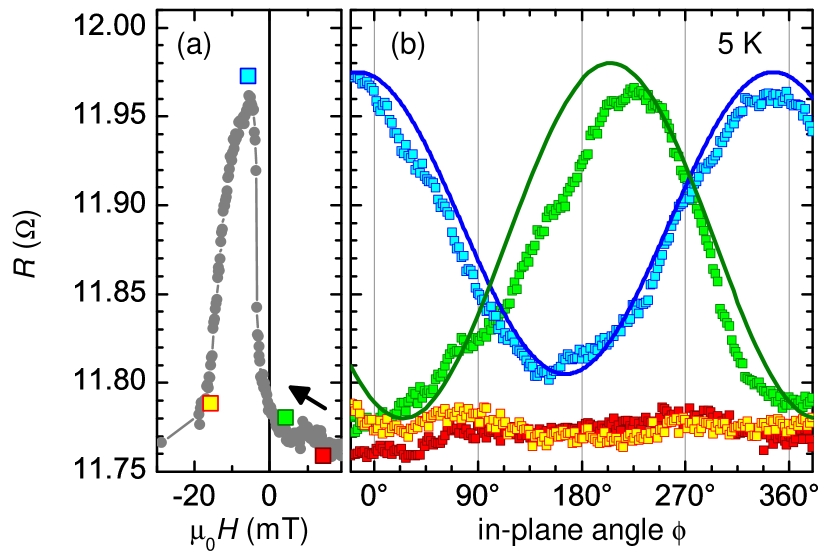
Above or below the coercivities of both Ni and Co electrodes, the resistance is low and does not vary significantly with (red and yellow symbols in Fig. 4(b)). This demonstrates that the magnetization directions in both ferromagnetic electrodes always stay aligned parallel and therefore follow the applied external field direction. For fields in between the coercivities of Ni and Co, however, the situation is different. displays a variation between its previously observed low value and a high resistive state with the same value as in the field sweep (Fig. 4(a)), following a behavior (green and blue symbols in Fig. 4(b)). This observation is in agreement with the assumption that the magnetization of the Co electrode (with lower coercivity) follows the external field direction whereas the magnetization of Ni (with higher coercivity) stays unaffected. This behavior is expected for a spin valve device as is the resulting dependence (green and blue lines in Fig. 4(b)). It is in clear contradiction to an anisotropic magnetoresistance (AMR) effect of the ferromagnetic electrodes which would result in a dependence.
Supplement II:
Interface resistance and spin selectivity
