Ga1-xMnxN epitaxial films with high magnetization
Abstract
We report on the fabrication of pseudomorphic wurtzite Ga−xMnxN grown on GaN with Mn concentrations up to 10 % using molecular beam epitaxy. According to Rutherford backscattering the Mn ions are mainly at the Ga-substitutional positions, and they are homogeneously distributed according to depth-resolved Auger-electron spectroscopy and secondary-ion mass-spectroscopy measurements. A random Mn distribution is indicated by transmission electron microscopy, no Mn-rich clusters are present for optimized growth conditions. A linear increase of the -lattice parameter with increasing Mn concentration is found using x-ray diffraction. The ferromagnetic behavior is confirmed by superconducting quantum-interference measurements showing saturation magnetizations of up to 150 emu/cm3.
pacs:
75.50.Pp, 75.60.Ej, 81.05.Ea, 81.15.HiDilute magnetic semiconductors (DMSs) ohno_window_2010 ; dietl_ten-year_2010 and particularly Mn-based nitrides, have been in the focus of research interest since the prediction that these systems may show hole-mediated room temperature ferromagnetism, if challenges associated with solubility limits, self-compensation, and the transition to a strong p-d coupling case are overcome.Dietl The potential of this type of materials to combine traditional electronics and photonics with the spin degree of freedom triggered the development of a number of potential applications.ohno_window_2010 ; Bader_Spintronics Especially Ga1-xMnxN is believed to be able to meet the conditions necessary for the implementation in devices, though the Mn solubility and the presence of compensating defects depend crucially on the growth conditions.Bonanni_transition_2007 It is now well established that because of the strong p-d hybridization, the Mn2+/3+ acceptor level occupies the mid band gap position in GaN.graf_prospects_2003 ; wolos_configuration_2009 Accordingly, in samples containing compensating donor centers, Mn ions assume the 2+ charge state, for which short range antiferromagnetic interactions dominate.zajac_paramagnetism_2001 ; granville_neighbour_2010 ; Bonanni_PRB_2011 In contrast, in uncompensated films, where Mn3+ ions prevail,Bonanni_PRB_2011 ; Sarigannidou_PRB_2006 ; Freeman_PRB_2007 ; Stefanowizc_PRB_2010 the net superexchange interactions become ferromagnetic, Bonanni_PRB_2011 ; Sarigannidou_PRB_2006 ; Kondo_JCG_2002 ; Sawicki_arXiv_2012 as predicted for Cr2+ in II-VI DMSs,Blinowski_PRB_1996 leading to Curie temperatures up to 8 K for 6 %.Bonanni_PRB_2011 ; Sawicki_arXiv_2012 It has been suggested that the presence of ferromagnetic interactions without band carriers, together with a sizable spin splitting of the excitonic states indicates the suitability of this dilute ferromagnetic insulators for magnetooptical devices, such as optical isolators. This has been already revealed for Ga1-xMnxN,PRB_Suffczynski_2011 where the destructive effect of antiferromagnetic interactions specific to II-VI Mn-based DMSs is circumvented.Zayets_JOptSoc_2005
In this letter, we report on the growth conditions that allow to obtain pseudomorph Ga1-xMnxN films containing up to 10 % of randomly distributed Mn ions using molecular beam epitaxy. In order to clarify the structural and magnetic properties of these samples, several investigation methods have been employed. The -axis lattice parameter of these films is found to obey Vegard’s law. Furthermore, the observed values of saturation magnetization up to 150 emu/cm3 are superior to other DMSs, such as (Ga,Mn)As.ohya_APL_2007 ; chiba_APL_2007 ; mack_APL_2008 ; wang_APL_2008
An EPI 930 molecular beam epitaxy (MBE) chamber equipped with a radio-frequency plasma source is used to deposit the Ga1-xMnxN layers. Templates consisting of 2 m GaN(0001) on c-plane sapphire fabricated by metal-organic vapor-phase epitaxy are used as substrates, the MBE grown layers are about 200 nm thick. All samples dicussed here are grown at a substrate temperature of 760 ∘C. At this temperature layer-by-layer growth is observed for metal-rich growth conditions. Mn acts as a surfactant for the growth, while excess material evaporates due to the comparatively low sticking coefficient of this element on GaN. In order to hinder the incorporation of Mn clusters within the layers, excessively metal-rich growth conditions are avoided during epitaxial deposition by carefully adjusting the Ga and Mn flux. Slightly metal-rich growth conditions close to the transition from two-dimensional to three-dimensional growth result in smooth layers without additional crystalline phases, while clusters are observed for highly Mn-rich conditions. A nitrogen flux of 1.3 standard cubic centimeters per minute at a plasma power of 300 W is used to provide atomic nitrogen. For each sample a beam equivalent pressure (BEP) of the Mn between 810-8 and 2.110-7 Torr was chosen, while the flux of the Ga cell is reduced from 210-6 Torr to 1.1510-7 Torr BEP. As the result, Ga1-xMnxN layers with Mn contents up to 10 % are obtained.
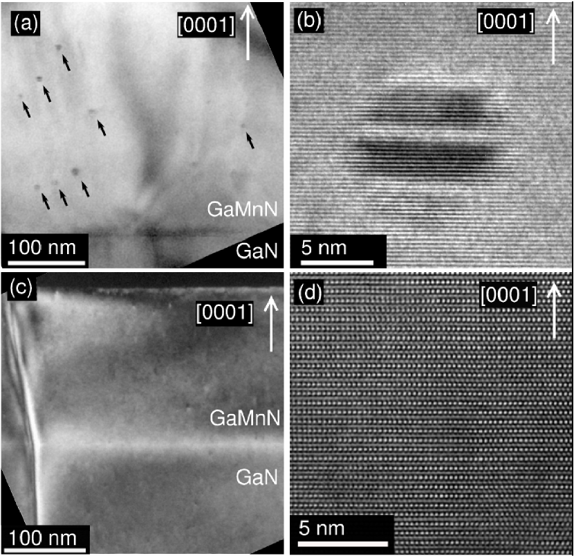
Transmission electron microscopy investigations have been carried out using a JEOL 2011 Fast TEM microscope operating at 200 kV. The samples are prepared by mechanical polishing. Afterwards ion polishing is used to flatten the surface of the specimen. Images in different magnification are depicted in Fig. 1. The sample shown in Fig. 1(a) and (b) is grown under highly Mn-rich growth conditions. Crystallographic phase separation is detected as Moiré fringes. In contrast, no indication of phase separation or cluster incorporation is found for the Ga1-xMnxN layers grown under slightly metal-rich conditions, as exemplarily shown in in Fig. 1(c) and (d), respectively. Mn is incorporated in a dilute manner solely in the wurtzite Ga1-xMnxN phase. Furthermore, no indication of an additional formation of threading dislocations was found in these layers. In the following, only the samples without phase separation will be discussed.
Auger electron spectroscopy (AES) as well as secondary ion mass spectrometry (SIMS) measurements have been carried out on selected samples to investigate the depth profile of Mn. In both methods Ar+ ions are used for sputtering. In SIMS the secondary ions are detected directly by a mass spectrometer. For AES the KLL transition is used to detect nitrogen, while the atomic fraction of Ga and Mn is determined by quantifying the LMM transition, respectively. Both curves shown in Fig. 2 reveal homogeneous elemental profiles for a typical sample containing a Mn content of about 10 %. The amount of Mn and Ga adds up to 50 % of the total number of atoms in a complementary manner, indicating Mn incorporation on Ga sites. The interface between Ga1-xMnxN layer and the GaN template layer at 0.2 m can clearly be identified as a step in the elemental concentrations in the depth profile. At this step the total number of Mn atoms per cubic centimeter drops five orders of magnitude to the noise level.
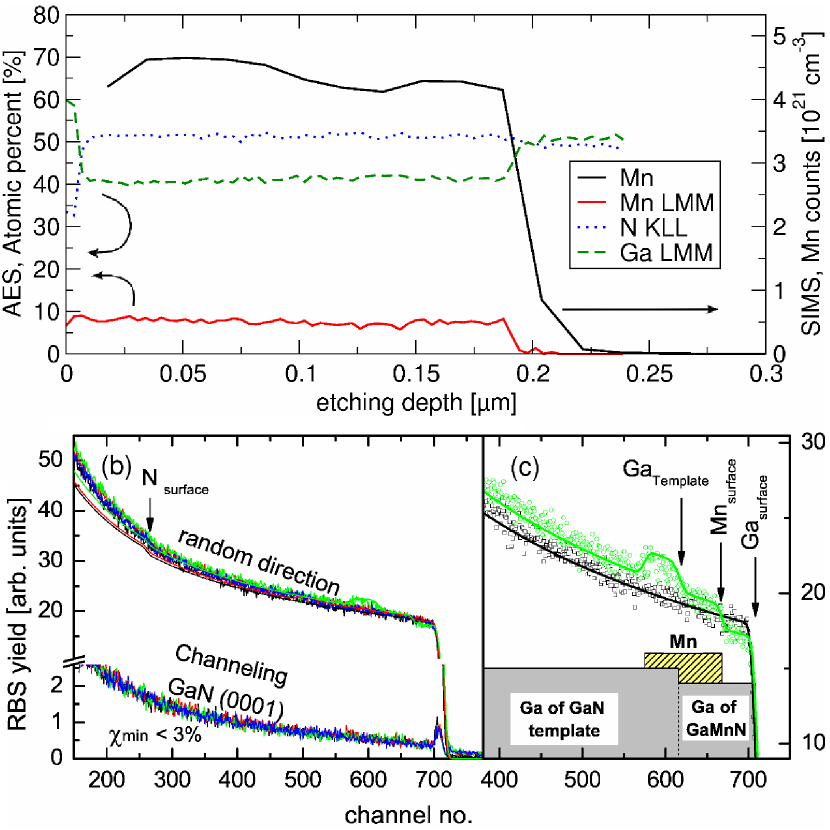
In order to clarify whether Mn atoms are also incorporated on interstitial lattice sites to a certain extent, Rutherford backscattering (RBS) measurements have been carried out. He atoms with energies of 1.7 MeV and full width at half maximum of 18 keV are accelerated in random and (0001) channeling direction. Samples with Mn concentrations from 0 % (pure GaN) to about 10 % are investigated in channeling mode as well as in random mode [Fig. 2(b)].
In channeling mode the channeling signal drops to approximately 3 % of the random signal; the samples are indistinguishable one from another indicating the high crystalline quality. These measurements confirm the low defect density in the samples. There are almost no interstitials detected in the (0001) channels. The amount of Mn incorporated has been determined by simulating the measured signal using an appropriate model, dividing the investigated sample into sublayers and calculating the energy spectrum of the backscattered He ions using the program code SIMNRA.website_simnra A magnification of the simulated elemental peaks is depicted in Fig. 2(c), exemplatory for the sample containing about 10 % Mn and pure GaN.
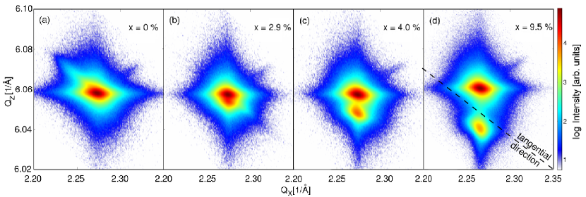
In order to verify a modification of the GaN lattice parameter induced by the Mn incorporation, high resolution x-ray diffraction (HRXRD) maps around the asymmetric (105)-reflex are performed as depicted in Fig. 3. These show two distinct features: the high intensity peaks at = 6.06 Å-1 are related to the GaN template layer while the lower intensity peak at smaller reciprocal lattice units origins from the thinner Ga1-xMnxN layer. The position of the peak shifts with increasing Mn content to smaller values of , i.e. larger lattice parameter. The peak of the Ga1-xMnxN layer has the same Qx position as the GaN template material, indicating a pseudomorphic growth. The orientation and shape of the Ga1-xMnxN layer peak changes with increasing Mn content. This behavior could be attributed to a change of the microstructure. At low Mn contents (Fig. 3b, 2.9 %) it is more a columnar like structure whereas at high Mn contents (Fig. 3d 10 %) the Ga1-xMnxN layer shows a strong mosaicity effect as this peak is mainly elongated along the tangential direction.Heinke Peak positions of 2 scans of the (0002)- and the (105)-reflex are used to determine the -lattice parameter for layers containing different Mn concentrations (not shown).
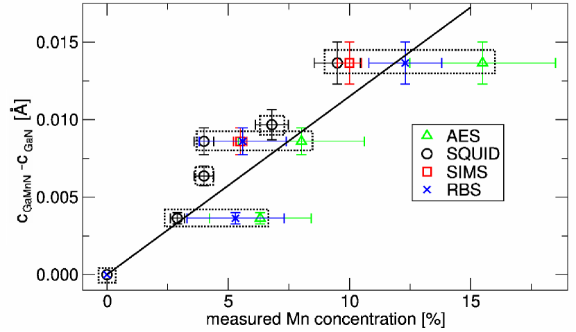
In Fig. 4, the deviation of the -lattice parameter of the Ga1-xMnxN-layer from the GaN template is plotted against the Mn content determined by the four different methods RBS, AES, SIMS and magnetometry employing a superconducting quantum interference measurements device (SQUID). Dashed rectangles indicate measurements belonging to the same sample. The vertical error bars represent the standard distribution of the spacing measured on different positions of the sample and comprises the error due to lateral inhomogeneities caused by a temperature gradient on the sample during growth. Vegard’s law describes a linear variation of lattice parameters with the composition of a mixed crystal (in relaxed state):
| (1) |
As the sampels are pseudomorphic the -lattice parameter is additionally elongated due to the elastic distortion of the unit cell. Taking all measurements without weighing into account we obtain a slope of 0.115(9) from a linear fit, where denotes the atomic Mn concentration as fraction of the total number of cation sites. Therefore, this formula can be used to determine the Mn content for Ga1-xMnxN samples in a convenient way using the non-destructive XRD method alone. For nano-wires an increase of the and -lattice parameter of and , respectively was calculated.GaMnN_nanowires Taking a ratio of the elastic constants of into account, these parameters result into an expected slope of for pseudomorphic material which is identical to our results within the error limits.Schuster_Strain_1999 For polycrystalline material a value of = 0.53 Å/ can be calculated from reference leite_nanocrystalline_2006, in the same manner, which deviates significantly.
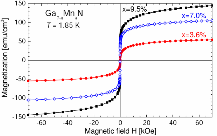
Magnetization measurements have been carried out down to a temperature of 1.85 K employing the commercial SQUID magnetometer MPMS XL–7 from Quantum Design and a measurement technique specifically developed in order to meaningfully examine thin layers of magnetically dilute semiconductors.Sawicki:2011_SST In Fig. 5 magnetization values measured up to 70 kOe for different Mn concentrations are depicted. While Curie temperatures are below 15 K in these samples, they show sizable saturation magnetizations of up to 150 emu/cm3 for the highest concentrations achieved. Such values are the highest ever reported for DMS, exceeding by 50 % those for (Ga,Mn)As.chiba_APL_2007 The detailed structural analysis presented before allows us to rule out a statistically significant contribution from secondary magnetic phases, pointing to Ga-substitutional Mn diluted in GaN as the sole source of this magnetization. The Mn concentration is determined by the near-saturation value of the magnetization at 70 kOe and 1.85 K, assuming that the value of the magnetic moment per Mn cation is 3.72 at these conditions, as implied by the group theoretical model for non-interacting Mn3+ cations.Stefanowizc_PRB_2010 ; Gosk_PRB_2005 As shown in Fig. 4, the values of obtained in this way are in a good agreement with other determinations of the Mn content.
In summary, we have successfully fabricated epitaxially dilute Ga1-xMnxN films. Extensive structural characterization excludes the presence of secondary crystalline phases or interstitial Mn atoms in samples obtained under appropriate growth conditions. A systematic modification of the -lattice parameter is observed with increasing Mn content, which is used to determine the parameters for Vegard’s law for this material for the pseudomorphic case. Magnetizations of up to 150 emu/cm3 are the highest reported for any DMS.
The authors would like to thank Dr. J. v. Borany for carrying out RBS measurements. This work was supported by the FunDMS Advanced Grant of the ERC (Grant No. 227690) within the Ideas 7th Framework Programme of European Community, by the InTechFun (Grant No. POIG.01.03.01-00-159/08), by the SemiSpinNet (Grant No. PITNGA-2008-215368), and by the Austrian FWF (P20065, P22477, P20550).
References
- (1) H. Ohno, Nat Mater 9, 952 (2010).
- (2) T. Dietl, Nat Mater 9, 965 (2010).
- (3) T. Dietl, H. Ohno, F. Matsukura, J. Cibert, and D. Ferrand, Science 287, 1019 (2000).
- (4) S. Bader and S. Parkin, Ann. Rev. Condens. Matter Phys. 1, 71 (2010).
- (5) A. Bonanni, Semicond. Sci. Tech. 22, R41 (2007).
- (6) T. Graf, S. T. B. Goennenwein, and M. S. Brandt, Phys. Stat. Sol. b 239, 277 (2003).
- (7) A. Wolos, M. Piersa, G. Strzeleka, K. Korona, A. Hruban, and M. Kaminska, Phys. Stat. Sol. c 6, 2769 (2009).
- (8) M. Zajac, J. Gosk, M. Kaminska, A. Twardowski, T. Szyszko, and S. Podsiadlo, Appl. Phys. Lett. 79, 2432 (2001).
- (9) S. Granville, B. J. Ruck, F. Budde, H. J. Trodahl, and G. V. M. Williams, Phys. Rev. B 81, 184425 (2010).
- (10) A. Bonanni, M. Sawicki, T. Devillers, W. Stefanowicz, B. Faina, T. Li, T. E. Winkler, D. Sztenkiel, A. Navarro-Quezada, M. Rovezzi, R. Jakieła, A. Grois, M. Wegscheider, W. Jantsch, J. Suffczyński, F. D’Acapito, A. Meingast, G. Kothleitner, and T. Dietl, Phys. Rev. B 84, 035206 (2011).
- (11) E. Sarigiannidou, F. Wilhelm, E. Monroy, R. M. Galera, E. Bellet-Amalric, A. Rogalev, J. Goulon, J. Cibert, and H. Mariette, Phys. Rev. B 74, 041306 (2006).
- (12) A. A. Freeman, K. W. Edmonds, N. R. S. Farley, S. V. Novikov, R. P. Campion, C. T. Foxon, B. L. Gallagher, E. Sarigiannidou, and G. van der Laan, Phys. Rev. B 76, 081201 (2007).
- (13) W. Stefanowicz, D. Sztenkiel, B. Faina, A. Grois, M. Rovezzi, T. Devillers, F. d’Acapito, A. Navarro-Quezada, T. Li, R. Jakieła, M. Sawicki, T. Dietl, and A. Bonanni, Phys. Rev. B 81, 235210 (2010).
- (14) T. Kondo, S. Kuwabara, H. Owa, and H. Munekata, J. Cryst. Growth 237-239, 1353 (2002).
- (15) M. Sawicki, T. Devillers, S. Gałȩski, C. Simserides, S. Dobkowska, B. Faina, A. Grois, A. Navarro-Quezada, K. N. Trohidou, J. A. Majewski, T. Dietl, and A. Bonanni, Phys. Rev. B 85, 205204 (2012).
- (16) J. Blinowski, P. Kacman, and J. A. Majewski, Phys. Rev. B 53, 9524 (1996).
- (17) J. Suffczyński, A. Grois, W. Pacuski, A. Golnik, J. A. Gaj, A. Navarro-Quezada, B. Faina, T. Devillers, and A. Bonanni, Phys. Rev. B 83, 094421 (2011).
- (18) V. Zayets, M. C. Debnath, and K. Ando, J. Opt. Soc. Am. B 22, 281 (2005).
- (19) S. Ohya, K. Ohno, and M. Tanaka, Appl. Phys. Lett. 90, 112503 (2007).
- (20) D. Chiba, Y. Nishitani, F. Matsukura, and H. Ohno, Appl. Phys. Lett. 90, 122503 (2007).
- (21) S. Mack, R. C. Myers, J. T. Heron, A. C. Gossard, and D. D. Awschalom, Appl. Phys. Lett. 92, 192502 (2008).
- (22) M. Wang, R. P. Campion, A. W. Rushforth, K. W. Edmonds, C. T. Foxon, and B. L. Gallagher, Appl. Phys. Lett. 93, 132103 (2008).
- (23) M. Mayer. simnra.com;http://home.rzg.mpg.de/~mam/References.html, (2001).
- (24) H. Heinke, M. Möller, D. Hommel, and G. Landwehr, J. Cryst. Growth 135, 41 (1994).
- (25) Y. P. Song, P. W. Wang, H. Q. Lin, G. S. Tian, J. Lu, Z. Wang, Y. Zhang, and D. P. Yu, J. Phys-Condens. Mat. 17, 5073 (2005).
- (26) M. Schuster, P. O. Gervais, B. Jobst, W. Hösler, R. Averbeck, H. Riechert, A. Iberl, and R. Stömmer, Journal of Physics D: Applied Physics 32, A56 (1999).
- (27) D. Leite, L. da Silva, A. Pereira, and J. Dias da Silva, J. Cryst. Growth 294, 309 (2006).
- (28) M. Sawicki, W. Stefanowicz, and A. Ney, Semicond. Sci. Technol. 26, 064006 (2011).
- (29) J. Gosk, M. Zajac, A. Wolos, M. Kaminska, A. Twardowski, I. Grzegory, M. Bockowski, and S. Porowski, Phys. Rev. B 71, 094432 (2005).