Antisite traps and metastable defects in Cu(In,Ga)Se2 thin-film solar cells
studied by screened-exchange hybrid density functional theory
Abstract
Electronic structure calculations within screened-exchange hybrid density functional theory show that antisites in both CuInSe2 and CuGaSe2 are localized hole traps, which can be attributed to the experimentally observed N2 level. In contrast, antisites and their defect complexes with copper vacancies exhibit an electron trap level, which can limit the open-circuit voltage and efficiency in Ga-rich Cu(In,Ga)Se2 alloys. Low-temperature photoluminescence measurements in CuGaSe2 thin-film solar cells show a free-to-bound transition at an energy of 1.48 eV, in very good agreement with the calculated transition energy for the antisite. Since the intrinsic DX center does not exhibit a pinning level within the band gap of CuInSe2, metastable DX behaviour can only be expected for antisites.
pacs:
88.40.jn, 66.30.Lw, 61.72.jj, 71.15.MbThin-film solar cells with aborbers based on Cu(In,Ga)Se2 alloys currenly achieve record efficiencies of 20.3% and represent one of the most promising technology for large-scale industrial production Jackson et al. (2011). Efficiencies up to 14.2% can also be obained with the ternary boundary phase CuInSe2, whereas the efficiencies of pure CuGaSe2 cells are still limited to below 10 % Caballero et al. (2007). Intrinsic point defects acting as recombination centers are likely to limit the open-circuit voltage and therefore the solar cell efficiency of these absorbers. The point defect physics of these chalcopyrites has been extensively studied by experimental methods, such as electrical and optical spectroscopy methods, and theoretical approaches, mostly calculations based on density functional theory Zhang et al. (1997, 1998); Wei et al. (1998); Zhao et al. (2004); Persson et al. (2005); Lany and Zunger (2005, 2006, 2008a); Pohl and Albe (2010); Pohl et al. (2011); Oikkonen et al. (2011). A hole trap level in the range between 0.15-0.35 eV, often named N2, has been observed using admittance and deep-level transient spectroscopy (DLTS) and Hall measurements in CuInSe2 Walter et al. (1996); Hanna et al. (2000); Mertens et al. (2007), CuGaSe2 Jasenek et al. (2000); Siebentritt and Rissom (2008); Mertens et al. (2007); Hanna et al. (2000); Krysztopa et al. (2011) and Cu(In,Ga)Se2 Herberholz et al. (1998); Schroeder et al. (1998); Heath et al. (2004); Walter et al. (1996); Hanna et al. (2000)). A measured activation energy between 0.05-0.20 eV, has been attributed to an interface defect in Cu(In,Ga)Se2 and was named N1 Herberholz et al. (1998), although this denomination is ambiguously used and it is unclear wether the N1 response is associated to a defect at all Eisenbarth et al. (2011). Indeed, various metastable effects have been oberserved in CIGSe devices such as persistent photoconductivity Meyer et al. (2002), the increase of the open-circuit voltage upon white-light soaking Ruberto and Rothwarf (1987), an increase of the space-charge upon illumination Igalson and Schock (1996) or reverse-biasing Herberholz et al. (1999) accompanied with a decrease of the fill factor Igalson et al. (2003) as well as capacitance relaxation on long time scales after light-soaking Engelhardt et al. (1998).
Based on electronic structure calculations within local density functional theory, two intrinsic point defects and their complexes with copper vacancies have been proposed to exhibit metastable properties in CuInSe2 and CuGaSe2: the intrinsic indium and gallium DX centers Lany and Zunger (2008a)111Intrinsic DX centers in CIGS can be regarded as antisites displaced to a three-fold coordinated off-lattice site, which may then act as recombination centers because they exhibit defect levels within the gap Lany and Zunger (2008a). and the selenium vacancy Lany and Zunger (2005) or selenium vacancy–copper vacancy complex Lany and Zunger (2006). These theoretical results have been invokedCwil et al. (2008); Urbaniak and Igalson (2009); Igalson et al. (2009); Siebentritt et al. (2010) to explain the experimentally observed light and voltage-bias induced metastabilities. However, metastable point defects are not the only possible explanation. Copper migration in the space charge regionBurgelman et al. (1997); Guillemoles et al. (2000), deep acceptor levels in the CdS buffer layerEisgruber et al. (1998), an electron-injection dependent barrier at the molybdenum back-contact of the device Eisenbarth et al. (2011), or the presence of a p+-layer in conjunction with a shallow donor level at the buffer absorber interfaceNiemegeers et al. (1998) have all been put forward as possible explanations. Therefore, metastabilities in Cu(In,Ga)Se2 based devices and their possible relation to the N2 and N1 levels remain puzzling and it is not clear whether a single explanation is sufficient to explain all of the observed phenomena Eisenbarth et al. (2011); Siebentritt (2011). Despite extensive efforts, no concise picture of the point defect physics that matches with all of the experimental findings has yet emerged.
In this letter, we show that antisites are localized hole traps in both CuInSe2 and CuGaSe2, which can be attributed to the experimentally observed N2 level, while antisites and their defect complexes with copper vacancies exhibit an electron trap level, which can limit the open-circuit voltage and efficiency in Ga-rich Cu(In,Ga)Se2 alloys. Our results are based on electronic structure calculations within screened-exchange hybrid density functional theory and are put in context to low-temperature photoluminescence measurements of CuGaSe2 thin-film solar cells.
We have carried out hybrid density functional calculations using the HSE06 functional Heyd et al. (2003, 2006) as implemented in VASPKresse and Furthmüller (1996) with an adapted exchange-screening parameter of 0.13 222The standard value for the fraction of exact exchange of 0.25 and a plane-wave energy cutoff of 350 eV was used., which allows to closely match the experimentally observed band gaps for both CuInSe2, CuGaSe2 and other chalcopyrite phasesPohl and Albe (2010). The approach allows to overcome the band-gap problem, to directly analyze defect levels within the gap and improves the description of localized and correlated copper electrons Lucero et al. (2011); Zhang et al. (2011). Thus, using the HSE06 functional will lead to more accurate formation enthalpies of point defects than LDA calculations. A 2x2x2 -centered k-point grid has been used for supercells with 64 atoms as well as with 216 atoms. Ion positions were relaxed until forces were converged to below 0.05 and 0.1 eV/Å, for supercells of 64 and 216 atoms, respectively. The calculation of supercells of 216 atoms with a 2x2x2 k-point grid are computationally extremely costly, but necessary in order to observe unambiguously localized defect levels of and . All reference phases presented in the stability diagram (Fig. 1) were calculated using the same functional. The point defect formation enthalpies were calculated as function of the chemical potentials of the constituents referenced to the elemental phases and the Fermi energy according to the common formula as e.g. in Ref. Persson et al. (2005). The potential alignment and image charge corrections have been carefully carried out as described in Ref. Lany and Zunger, 2008b.
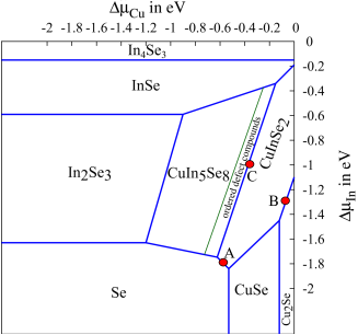
Since high-efficiency Cu(In,Ga)Se2 absorber material is prepared under a highly selenium-rich atmosphere, e.g. with a selenium to metal flux ratio of 5 Hanna et al. (2003), it is instructive to interpret the defect physics for this material under selenium-rich conditions on the Se-Cu(In,Ga)Se2 phase boundary in the calculated stability diagram (point A in Fig. 1). In contrast to a previously calculated stability diagram Persson et al. (2005), our calculations show a phase boundary between Cu2Se and CuInSe2, which is in line with the experimental phase diagram and the observation of Cu2Se precipitates under certain processing conditionsHaalboom et al. (1998) (point B). For Cu-poor compositions, which yield the highest conversion efficiency, Cu(In,Ga)Se2 is a highly compensated semiconductor. In this case, the charge neutrality condition and thus the Fermi-energy is essentially determined by the concentration of donors and acceptors with the lowest formation energies (see Fig. 2). For the chemical potentials at points A, B and C the material turns out to be p-type, while it becomes n-type for maximal Cu- and In-rich conditions (not shown). Fig. 2 shows the calculated defect formation enthalpies for the various chemical potentials.
One of the most intriguing result is that antisites in both materials, CuInSe2 and CuGaSe2, can have equally low formation enthalpies as copper vacancies and thus also act as compensating defects. This finding is consistent with large concentrations of in recently reported using wavelength dispersive x-ray diffraction even for copper-poor material Stephan et al. (2011). However, when the chemical potentials are shifted towards metal-rich conditions (e.g. point C), it is seen that the formation enthalpy of at the intrinsic Fermi level (vertical arrow) increases, while it does not change much for and .
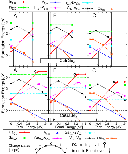
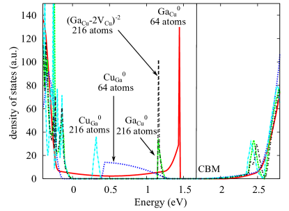
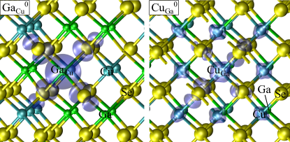
The analysis of the density of states of and reveals an empty narrow defect band above the VBM for in CuInSe2 (at 0.27 eV) and in CuGaSe2 (at 0.32 eV), which can trap two holes (the hole density of the empty single-particle defect state of as obtained from the calculation is displayed in Fig. 4). Furthermore, a localized electron trap level emerges for at a single-particle energy of 1.17 eV above the VBM in CuGaSe2 (see also Fig. 4). Forming defect complexes such as and , does not affect the position of the defect level. The defect level of is found to be resonant within the CB for CuInSe2 at 1.48 eV and for CuGaSe2 at 1.46 eV approximately independent of gallium content. All individual single-particle defect levels are approximately constant on an absolute energy scale, when comparing their position in CuInSe2 and CuGaSe2 relative to the respective VBM. However, the defect levels of and as individual defects do not align on an absolute scale, the defect level being 0.29-0.41 eV higher than the one of in both CuInSe2 and CuGaSe2 as host material.
Here it should be noted that defect calculations on Cu(In,Ga)Se2 have so far been performed with supercells smaller or equal to 64 atoms. However, very disperse defect bands appear within the gap for the cells with 64 atoms (see Fig. 3), which indicates significant self-overlap of the defect wavefunctions. If local or semilocal density functionals are used, delocalization also occurs in large supercells up to 216 atom, which is why localized deep hole traps have not been identified in the past. This proves that an accurate nonlocal treatment of exchange and correlation and large supercells are crucial for obtaining the correct localization behaviour of the defect.
The antisites localize holes, are abundant under typical preparation conditions (up to at 850 K deposition temperature and the calculated thermal transition energy for the process of 0.20 eV agrees with experimental measurements (e.g. 0.1-0.3 eV in Ref. Heath et al. (2004) and 0.1-0.2 eV in Ref. Schroeder et al. (1998)). Given these evidences it is safe to conclude that the N2 hole trap level is due to the antisite. The fact that this level does not occur in all samples can be explained with differing formation enthalpies relevant for different preparation conditions (compare points A,B,C in Fig. 2).
The antisite, in contrast, shows a clearly localized electron trap level at a single-particle energy of 1.17 eV above the VB in CuGaSe2 and at 1.07 eV in CuInSe2 very close to the CBM. Therefore this antisite defect becomes increasingly deep when Ga is alloyed into CuInSe2, due to the rising CB. Since is expected to occur in large quantities in due to its low formation enthalpy, it may limit solar cell efficiency when Ga alloying is used to increase the band-gap: When the CBM is raised above the position of the defect level, recombination through this defect may limit the open-circuit voltage. Since the associates of with copper vacancies display the same single-particle defect level as the non-complexed antisite, the complexes may cause the same limitations. With regard to the defect complexes we find that their formation enthalpies are not particularly low (Fig. 2). In fact, the total binding energy of the complexes with respect to the isolated charged species is only about 0.3 eV.
It might be tempting to relate the experimentally observed N1 signature to the normal configuration of the defect in . However, we note that such an assignment is contradicted by the observation of N1 in pure and the fact that its activation energy does not change with increasing Ga-content Eisenbarth et al. (2009); Turcu et al. (2001).
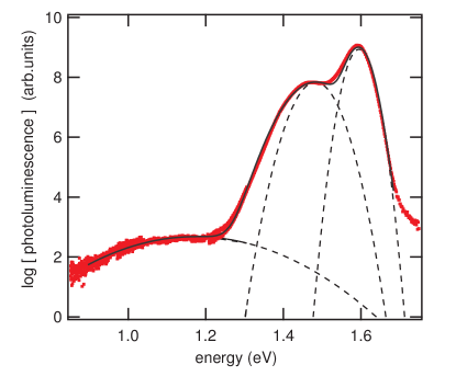
To confirm our theoretical results for the defect, we conducted temperature-dependent photoluminescence measurements on a CuGaSe2 thin-film solar cells prepared by a three-stage coevaporation process, as used for high-efficiency chalcopyrite solar cell devicesCaballero et al. (2007). For the thin film absorber investigated, a ratio [Cu]/[Ga] = 0.87 was measured by x-ray fluorescence analysis and the accompanying solar cell showed a device efficiency of 7%. Photoluminescence (PL) was measured using a 670 nm diode-laser as excitation source and a thermoelectrically-cooled InGaAs array coupled to a 0.5 m spectrograph for luminescence detection, with the sample placed in a closed-cycle helium cryostat. A photoluminescence spectrum obtained at 15 K is shown in Fig. 5. Three recombination peaks located at 1.6 eV, 1.48 eV and 1.17 eV can be clearly distinguished. The temperature and excitation intensity dependence of these peaks is consistent with an assignment of the peak at 1.6 eV to a tail-to-band transition, commonly observed in Cu-poor chalcopyrites Krustok et al. (1999), and the assignment of the peak at 1.48 eV to a free-to-bound transition. The latter transition energy is in excellent agreement with the calculated optical emission energy for the recombination process in (1.44 eV) 333Since Koopman’s theorem does not apply in density functional theory, the single-particle energies may differ from absorption and photoluminescence energies.. The temperature and excitation dependence of the third broad peak observed at about 1.17 eV is consistent with a donor-acceptor transition. A possible candidate for this transition is the process , i.e. the recombination of a single electron localized on a antisite with a neighbouring hole trap by radiative tunneling, which has a calculated transition energy of 1.02 eV.
For metastabilities originating from intrinsic DX centers to occur, it is necessary that a DX pinning level exists within the gapLany and Zunger (2008a). From our results (Fig. 2), we conclude that such a pinning level only occurs for antisites in CuGaSe2 (), but not for antisites in CuInSe2 (, well above the CB). Therefore, Fermi-level pinning and metastable effects due to intrinsic DX centers may occur in larger band gap Cu(In,Ga)Se2 materials, but not for the ternary CuInSe2. In order to assess the energy differences responsible for the different DX pinning levels as compared to Ref. Lany and Zunger (2008a), it is instructive to compare the uncorrected formation enthalpies of and in CuInSe2 within our approach to the ones obtained from LDA applying only the static +U valence band correction of Ref. Lany and Zunger (2008a), which we were able to reproduce. The uncorrected formation enthalpy of within our approach is 0.4 eV lower, while the one of is 0.32 eV higher. These energy differences, which result from the different treatments of exchange and correlation within HSE06 as compared to the LDA, which result mostly from the improved description of the Cu electrons, directly cause the change in the DX pinning levels.
We have also investigated vacancy pairs, which have been held responsible for a variety of metastability phenomena in Cu(In,Ga)Se2. With respect to this defect pair our hybrid functional calculations yield comparable charge transition levels (+/-) and metastable relaxation behavior as previously found in LDA-based calculations Lany and Zunger (2006). However, the formation enthalpies of this defect complex are higher than 2 eV at the relevant Fermi levels at points A,B and C in Fig. 2). Thus, under thermal equilibrium conditions, associates should occur only in minor quantities (below at 850 K deposition temperature as estimated from the formation enthalpies). Thus, these defects can only cause metastable phenomena if the material is prepared under far-from-equilibrium conditions.
In conclusion, we have shown that defects create a localized hole trap level in both CuInSe2 and CuGaSe2. Given the large amount of experimental evidence for a hole trap level in the range 0.15-0.35 eV, we conclude that defects should be assigned to the N2 level. and its complexes display a localized defect level within the gap in CuGaSe2 and CuInSe2. These defects are thus a likely cause for the limited efficiency of CuGaSe2 based wide band devices. Since does not exhibit a Fermi pinning level in CuInSe2, metastable DX behaviour can only be expected for antisites.
We acknowledge useful discussions with Dr. Péter Ágoston and Prof. Andreas Klein (TUD), Dr. R. Caballero for CuGaSe2 sample growth, S. Kretschmar for the photoluminescence measurements, grants of computer time on JUROPA at the Jülich Supercomputing Center and funding within the GRACIS project (BMBF).
References
- Jackson et al. (2011) P. Jackson, D. Hariskos, E. Lotter, S. Paetel, R. Wuerz, R. Menner, W. Wischmann, and M. Powalla, Prog. Photovoltaics 19, 894 (2011).
- Caballero et al. (2007) R. Caballero, C. A. Kaufmann, M. Cwil, C. Kelch, D. Schweigert, T. Unold, M. Rusu, H. W. Schock, and S. Siebentritt, J. Phys. Cond. Matter 19, 356222 (2007).
- Zhang et al. (1997) S. Zhang, S. Wei, and A. Zunger, Phys. Rev. Lett. 78, 4059 (1997).
- Zhang et al. (1998) S. Zhang, S.-H. Wei, A. Zunger, and H. Katayama-Yoshida, Phys. Rev. B 57, 9642 (1998).
- Wei et al. (1998) S.-H. Wei, S. Zhang, and A. Zunger, Appl. Phys. Lett. 72, 3199 (1998).
- Zhao et al. (2004) Y. Zhao, C. Persson, S. Lany, and A. Zunger, Appl. Phys. Lett. 85, 5860 (2004).
- Persson et al. (2005) C. Persson, Y.-J. Zhao, S. Lany, and A. Zunger, Phys. Rev. B 72, 035211 (2005).
- Lany and Zunger (2005) S. Lany and A. Zunger, Phys. Rev. B 72, 035215 (2005).
- Lany and Zunger (2006) S. Lany and A. Zunger, J. Appl. Phys. 100, 113725 (2006).
- Lany and Zunger (2008a) S. Lany and A. Zunger, Phys. Rev. Lett. 100, 016401 (2008a).
- Pohl and Albe (2010) J. Pohl and K. Albe, J. Appl. Phys. 108, 023509 (2010).
- Pohl et al. (2011) J. Pohl, A. Klein, and K. Albe, Phys. Rev. B 84, 121201 (2011).
- Oikkonen et al. (2011) L. E. Oikkonen, M. G. Ganchenkova, A. P. Seitsonen, and R. M. Nieminen, J. Phys. Cond. Matter 23, 422202 (2011).
- Walter et al. (1996) T. Walter, R. Herberholz, C. Muller, and H. W. Schock, Journal of Applied Physics 80, 4411 (1996).
- Hanna et al. (2000) G. Hanna, A. Jasenek, U. Rau, and H. W. Schock, Phys. Status Solidi A 179, R7 (2000).
- Mertens et al. (2007) V. Mertens, J. Parisi, and R. Reineke-Koch, J. Appl. Phys. 101, 104507 (2007).
- Jasenek et al. (2000) A. Jasenek, U. Rau, V. Nadenau, and H. W. Schock, J. Appl. Phys. 87, 594 (2000).
- Siebentritt and Rissom (2008) S. Siebentritt and T. Rissom, Appl. Phys. Lett. 92, 062107 (2008).
- Krysztopa et al. (2011) A. Krysztopa, M. Igalson, P. Zabierowski, J. Larsen, Y. Aida, S. Siebentritt, and L. Guetay, Thin Solid Films 519, 7308 (2011).
- Herberholz et al. (1998) R. Herberholz, M. Igalson, and H. W. Schock, J. Appl. Phys. 83, 318 (1998).
- Schroeder et al. (1998) D. J. Schroeder, J. L. Hernandez, G. D. Berry, and A. A. Rockett, J. Appl. Phys. 83, 1519 (1998).
- Heath et al. (2004) J. T. Heath, J. D. Cohen, and W. N. Shafarman, J. Appl. Phys. 95, 1000 (2004).
- Eisenbarth et al. (2011) T. Eisenbarth, R. Caballero, M. Nichterwitz, C. Kaufmann, H. Schock, and T. Unold, J. Appl. Phys. 110, 094506 (2011).
- Meyer et al. (2002) T. Meyer, F. Engelhardt, J. Parisi, and U. Rau, Journal of Applied Physics 91, 5093 (2002).
- Ruberto and Rothwarf (1987) M. Ruberto and A. Rothwarf, J. Appl. Phys. 61, 4662 (1987).
- Igalson and Schock (1996) M. Igalson and H. W. Schock, J. Appl. Phys. 80, 5765 (1996).
- Herberholz et al. (1999) R. Herberholz, U. Rau, H. Schock, T. Haalboom, T. Godecke, F. Ernst, C. Beilharz, K. Benz, and D. Cahen, Eur. Phys. J.: Appl. Phys. 6, 131 (1999).
- Igalson et al. (2003) M. Igalson, M. Bodegard, L. Stolt, and A. Jasenek, Thin Solid Films 431, 153 (2003).
- Engelhardt et al. (1998) F. Engelhardt, M. Schmidt, T. Meyer, O. Seifert, J. Parisi, and U. Rau, Physics Letters A 245, 489 (1998).
- Note (1) Intrinsic DX centers in CIGS can be regarded as antisites displaced to a three-fold coordinated off-lattice site, which may then act as recombination centers because they exhibit defect levels within the gap Lany and Zunger (2008a).
- Cwil et al. (2008) M. Cwil, M. Igalson, P. Zabierowski, and S. Siebentritt, J. Appl. Phys. 103, 06370119 (2008).
- Urbaniak and Igalson (2009) A. Urbaniak and M. Igalson, J. Appl. Phys. 106, 063720 (2009).
- Igalson et al. (2009) M. Igalson, A. Urbaniak, and M. Edoff, Thin Solid Films 517, 2153 (2009).
- Siebentritt et al. (2010) S. Siebentritt, M. Igalson, C. Persson, and S. Lany, Prog. Photovoltaics 18, 390 (2010).
- Burgelman et al. (1997) M. Burgelman, F. Engelhardt, J. F. Guillemoles, R. Herberholz, M. Igalson, R. Klenk, M. Lampert, T. Meyer, V. Nadenau, A. Niemegeers, et al., Prog. Photovoltaics 5, 121 (1997).
- Guillemoles et al. (2000) J.-F. Guillemoles, L. Kronik, D. Cahen, U. Rau, A. Jasenek, and H.-W. Schock, J. Phys. Chem. B 104, 4849 (2000).
- Eisgruber et al. (1998) I. Eisgruber, J. Granata, J. Sites, J. Hou, and J. Kessler, Solar Energy Materials and Solar Cells 53, 367 (1998).
- Niemegeers et al. (1998) A. Niemegeers, M. Burgelman, R. Herberholz, U. Rau, D. Hariskos, and H. W. Schock, Progress In Photovoltaics 6, 407 (1998).
- Siebentritt (2011) S. Siebentritt, Solar Energy Materials and Solar Cells 95, 1471 (2011).
- Heyd et al. (2003) J. Heyd, G. Scuseria, and M. Ernzerhof, J. Chem. Phys. 118, 8207 (2003).
- Heyd et al. (2006) J. Heyd, G. Scuseria, and M. Ernzerhof, J. Chem. Phys. 124, 219906 (2006).
- Kresse and Furthmüller (1996) G. Kresse and J. Furthmüller, Phys. Rev. B 54, 11169 (1996).
- Note (2) The standard value for the fraction of exact exchange of 0.25 and a plane-wave energy cutoff of 350 eV was used.
- Lucero et al. (2011) M. J. Lucero, I. Aguilera, C. V. Diaconu, P. Palacios, P. Wahnón, and G. E. Scuseria, Phys. Rev. B 83, 205128 (2011).
- Zhang et al. (2011) Y. Zhang, X. Yuan, X. Sun, B.-C. Shih, P. Zhang, and W. Zhang, Phys. Rev. B 84, 075127 (2011).
- Lany and Zunger (2008b) S. Lany and A. Zunger, Phys. Rev. B 78, 235104 (2008b).
- Hanna et al. (2003) G. Hanna, J. Mattheis, V. Laptev, Y. Yamamoto, U. Rau, and H. Schock, Thin Solid Films 431-432, 31 (2003).
- Haalboom et al. (1998) T. Haalboom, T. Godecke, F. Ernst, M. Ruhle, R. Herberholz, H. W. Schock, C. Beilharz, and K. W. Benz, Inst. Phys. Conf. Ser. 152, 249 (1998).
- Stephan et al. (2011) C. Stephan, S. Schorr, M. Tovar, and H. W. Schock, Appl. Phys. Lett. 98, 091906 (2011).
- Heath et al. (2002) J. T. Heath, J. D. Cohen, W. N. Shafarman, D. X. Liao, and A. A. Rockett, Appl. Phys. Lett. 80, 4540 (2002).
- Eisenbarth et al. (2009) T. Eisenbarth, T. Unold, R. Caballero, C. A. Kaufmann, D. Abou-Ras, and H. . W. Schock, Thin Solid Films 517, 2244 (2009).
- Turcu et al. (2001) M. Turcu, I. M. Kötschau, and U. Rau, Appl. Phys. A 73, 769 (2001).
- Krustok et al. (1999) J. Krustok, M. Collan, M. Yakushev, and K. Hjelt, Physica Scripta T79, 179 (1999).
- Note (3) Since Koopman’s theorem does not apply in density functional theory, the single-particle energies may differ from absorption and photoluminescence energies.