Supercurrent in Nb/InAs-Nanowire/Nb Josephson junctions
Abstract
We report on the fabrication and measurements of planar mesoscopic Josephson junctions formed by InAs nanowires coupled to superconducting Nb terminals. The use of Si-doped InAs-nanowires with different bulk carrier concentrations allowed to tune the properties of the junctions. We have studied the junction characteristics as a function of temperature, gate voltage, and magnetic field. In junctions with high doping concentrations in the nanowire Josephson supercurrent values up to 100 nA are found. Owing to the use of Nb as superconductor the Josephson coupling persists at temperatures up to 4 K. In all junctions the critical current monotonously decreased with the magnetic field, which can be explained by a recently developed theoretical model for the proximity effect in ultra-small Josephson junctions. For the low-doped Josephson junctions a control of the critical current by varying the gate voltage has been demonstrated. We have studied conductance fluctuations in nanowires coupled to superconducting and normal metal terminals. The conductance fluctuation amplitude is found to be about 6 times larger in superconducting contacted nanowires. The enhancement of the conductance fluctuations is attributed to phase-coherent Andreev reflection as well as to the large number of phase-coherent channels due to the large superconducting gap of the Nb electrodes.
I Introduction
Coherent transport in mesoscopic semiconductor-based Josephson junctions has been attracting a lot of interest from fundamental and applied physics point of view. Modern nanofabrication techniques provide a possibility to fabricate planar multi-terminal Josephson structures relevant for the realization of different types of hybrid superconductor/semiconductor nanoscale devices.De Franceschi et al. (2010); Schäpers (2001) Josephson field effect transistors,Akazaki et al. (1996) superconducting quantum point contacts Takayanagi et al. (1995a) and injection current controlled Josephson junctions Schäpers et al. (2003) were realized with high-mobility 2-dimensional electron gases in semiconductor heterostructures. Recently, the Josephson effect was also observed in nanoscale devices formed by semiconductor nanowires coupled to superconducting terminals. Doh et al. (2005); Xiang et al. (2006); van Dam et al. (2006); Frielinghaus et al. (2010); Roddaro et al. (2011); De Franceschi et al. (2010); Nishio et al. (2011)
Up to now, most of experimental studies of semiconductor-based Josephson junctions at nanoscale have been focused on structures with an InAs-nanowire as a semiconductor weak link. Experiments show that a charge accumulation layer is formed at the surface of the InAs, Smit et al. (1989) which provides a sufficiently low resistive contact to superconducting electrodes. It was found that highly transparent contacts are formed at the interfaces between the InAs nanowire and Al superconducting electrodes. At temperatures below 1 K the high transparency of the contacts gives rise to proximity-induced superconductivity. A large number of experiments have been carried out on Al/InAs-nanowire junctions, demonstrating tunable Josephson supercurrentsDoh et al. (2005); Xiang et al. (2006), supercurrent reversal,van Dam et al. (2006) Kondo enhanced Andreev tunneling,Sand-Jespersen et al. (2007) and suppression of supercurrent by hot-electron injection.Roddaro et al. (2011) Furthermore, gate-controlled superconducting quantum interference devices, van Dam et al. (2006); De Franceschi et al. (2010) and tunable Cooper pair splittersHofstetter et al. (2009) have been realized.
The use of Al as a superconductor in nanowire-based Josephson junctions limits the operation temperature of the nanofabricated devices below K. To extend the operation of the Josephson devices at higher temperatures, it has been suggested to use superconductors which have higher temperatures of superconducting transition. Recently, Spatnis et al. Spathis et al. (2011) have realized proximity dc SQUIDs based on InAs nanowires and vanadium superconducting electrodes ( K). It is shown that V/InAs-nanowire/V Josephson junctions can operate at temperatures up to 2.5 K. Furthermore, for InN-nanowire-based junctions with Nb electrodes ( K) a Josephson supercurrent was observed up to temperatures of K.Frielinghaus et al. (2010) It is also pointed out that, owing to the strong spin-orbit coupling in InAs nanowires,Fasth et al. (2007) the mesoscopic devices fabricated could be used for the experimental demonstration of Majorana fermions Lutchyn et al. (2010).
In some aspects small-size planar superconductor/normal conductor/superconductor Josephson junctions differ significantly from their large-size counterparts, i.e. the magnetic field dependence of the critical current is expected to decrease monotonously with increasing magnetic field in contrast to the Fraunhofer-type vs. dependence for larger junctions.Cuevas and Bergeret (2007); Bergeret and Cuevas (2008) Indeed, a monotonous decrease of was recently observed in Nb/Au/Nb and Al/Au/Al junctions as well as in Nb/InN-nanowire/Nb junctions.Angers et al. (2008); Frielinghaus et al. (2010) Furthermore, in junctions with a semiconductor nanowire in between two superconducting electrodes mesoscopic effects, i.e. conductance fluctuations and fluctuations of the critical current have been observed when the gate voltage is varied. Doh et al. (2005, 2008); Jespersen et al. (2009) The gate voltage dependent conductance fluctuations measured at finite bias voltage were shown to follow almost precisely the fluctuations of the supercurrent Takayanagi et al. (1995b); Doh et al. (2005). It was also found that the conductance fluctuation amplitude measured at bias voltages lower than 2/e significantly exceeds the amplitude of the normal-state universal conductance fluctuations.Doh et al. (2008); Jespersen et al. (2009)
In our study we investigated the Josephson effect in Nb/InAs-nanowire/Nb hybrid structures. By using InAs-nanowires with two different bulk carrier concentrations we were able to vary the properties of the nanoscale weak link Josephson junction to a large extent, i.e. in the junctions with the highly doped InAs nanowires a relatively large Josephson supercurrent is observed, whereas for junctions with low doped nanowires is reduced but here a gate control of the superconducting switching currents is possible. We devoted special attention to effects which originate from the small size of the junctions, in particular the magnetic field dependence of the critical current as well as the gate voltage dependent conductance and supercurrent fluctations. The field dependence of the critical current and the fluctuation phenomena are compared to recent theoretical models.
II Experimental
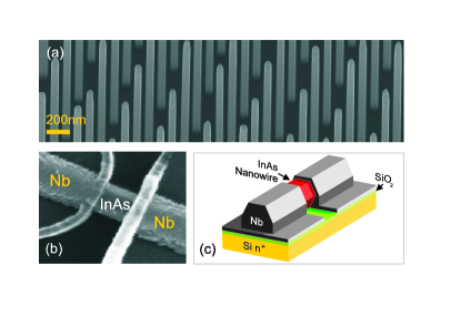
The -type doped InAs nanowires were grown by selective area metal organic vapor phase epitaxy (MOVPE) without using catalyst material. In order to tune the Si doping level, the ratio of disilane (Si2H6) partial pressure and group III precursor has been adjusted as , which is defined as doping factor 1. In this study we have used nanowires with two different doping concentrations.Wirths et al. (2011) The resistivity for the lower (doping factor 100, carrier concentration cm-3) and higher doped (doping factor 500, cm-3) nanowires was 0.019 and 0.0018 cm, respectively. In Fig. 1(a) a scanning electron micrograph of the as-grown nanowires is shown. Detailed information concerning the growth and characterization of the doped nanowires can be found elsewhere.Wirths et al. (2011) The samples are labeled as ”L1, L2” and ”H1, H2” for junctions based on a nanowire with lower (doping factor 100) or higher (doping factor 500) doping concentration, respectively.
In order to contact the nanowires with Nb electrodes they were transferred from the growth substrate to an -Si/SiO2 substrate with predefined electron beam markers. The Nb electrodes were defined by electron beam lithography and lift-off. Before Nb deposition the samples were exposed to an oxygen plasma to remove electron beam resist residues on the contact area. Furthermore, in order to obtain a high contact transparency, Ar+ ion milling was employed to remove the native oxide on the nanowire surface. The 100 nm thick Nb layer was deposited by sputtering. The highly doped -type substrate was used for back-gating of the nanowires. A scanning electron micrograph of a typical junction (sample L2) is shown in Fig. 1(b), while a schematics of the junction lay-out can be found in Fig. 1(c). The contact separations of the four different samples are given in 1. The transport measurements were performed at temperatures down to 0.3 K in a He-3 cryostat equipped with a superconducting solenoid with a magnetic field up to 7 T. The DC and differential current-voltage characteristics were measured using a four-terminal current-driven measurement scheme. Current and voltage leads were filtered by RC filters thermally anchored at 2 K. The differential resistance was measured with a lock-in amplifier by superimposing a small AC signal of 5 nA to the junction bias current.
III Results and Discussion
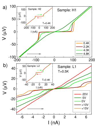
In Fig. 2(a) the current-voltage () characteristics at various temperatures between 0.4 and 4.8 K are shown for a sample with a highly doped nanowire (sample H1). At temperatures K and small bias, a clear Josephson supercurrent is observed in the junction. As the bias current exceeds a certain value , the Josephson junction switches from the superconducting to the normal state. The switching current measured at 0.4 K for the sample H1 is about 100 nA. With increasing the temperature is reduced. At K the supercurrent is suppressed completely. Our measurements show that at temperatures below 2 K the -characteristics are hysteretic. With increasing the temperature the hysteresis is gradually suppressed. The retrapping current , defined by the switching from the normal state back into the superconducting state, has a value of 84 nA at 0.4 K and remains almost constant when the temperature is increased to 2 K. As can be inferred from the -characteristics shown in Fig. 2(a) (inset) the switching current of the second sample with the highly doped nanowire (sample H2) has a somewhat smaller value of 70 nA compared to the first sample.
It should be noted that the switching current is strongly affected by the external on-chip circuit integrated with the Josephson junctionJarillo-Herrero et al. (2006); Pallecchi et al. (2008); Jespersen et al. (2009) and depends on the quality factor of the devices. Following the approach given in Refs.Jarillo-Herrero et al. (2006); Jespersen et al. (2009) we have estimated the quality factor of the samples H1, H2 taking into account the electromagnetic environment. Estimations show that , thus, the junctions H1, H2 are in the overdamped limit and the measurable supercurrent approaches the thermodynamic critical current . The observed hysteresis in the characteristics in our planar mesoscopic SNS Josephson junctions can be explained by the increase of the electron temperature in the weak link once the junction switches to the resistive state.Courtois et al. (2008)
Due to the lower electron concentration, gate control was achieved for the samples with the lower doped nanowires. For sample L1 this is shown in Fig. 2(b), where the -characteristics at 0.5 K are plotted for back-gate voltages between V and V. At zero gate voltage the measured is about 2.8 nA, which is considerably smaller than the of the junctions with the highly doped nanowires. We attribute the lower to the larger resistivity of the lower doped nanowires. As can be seen in Fig. 1(b), by applying a back-gate voltage of V the switching current can be increased by about a factor of 2. The larger value of the switching current is due to the fact that by applying a positive gate voltage the electron concentration in the nanowires is increased so that the resistivity is decreased. In contrast, by applying a negative gate voltage the electron concentration in the nanowire is reduced. As a consequence, is reduced [cf. Fig. 2(b)], and at a gate voltage of V the supercurrent is suppressed completely. As can be seen in Fig. 2(b), a small voltage drop appears for currents below which can be attribute thermal smearing. A Josephson supercurrent was also observed for the second sample with a low doped nanowire (sample L2) [cf. Fig. 2(b) (inset)]. Here, is found to be 12 nA at 0.4 K and thus larger than the value for sample L1. As discussed in detail below, for sample L2 a gate control of was obtained as well.
| Device | (nm) | (nm) | (k) | (nA) |
|---|---|---|---|---|
| Sample H1 | 140 | 110 | 0.75 | 100 |
| Sample H2 | 160 | 100 | 0.90 | 70 |
| Sample L1 | 70 | 80 | 3.8 | 2.8 |
| Sample L2 | 85 | 75 | 2.5 | 12 |
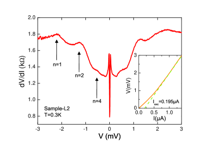
In Fig. 3, the differential resistance vs bias voltage of the sample L2 is shown. The measurement temperature was 0.3 K. The peaks in at finite bias voltages can be associated with the subharmonic energy gap structure caused by multiple Andreev reflections, with peak positions given by .Octavio et al. (1983); Flensberg et al. (1988); Cuevas et al. (2006) From the fit of the peak positions we have determined the superconducting energy gap in the Nb leads meV and found that the observed peaks correspond to and 3. The contact transparency in the device L2 can be estimated using the -characteristic for .Xiang et al. (2006); Nishio et al. (2011) We have found that the fit to the -curve at the normal state in the range mV extrapolates to a finite excess current nA as shown in the inset of Fig. 2. Using the superconducting energy gap meV and the normal state resistance of the junction k, we obtain =0.4. We analyzed the data within the framework of the standard Blonder-Tinkham-Klapwijk (BTK) theory.Blonder et al. (1982) The obtained value is converted to the BTK barrier strength parameter ,Flensberg et al. (1988) which corresponds to a contact transparency . Subgap features as found here have been observed before in other superconductor-semiconductor junctions.Frielinghaus et al. (2010); Batov et al. (2004); Chrestin et al. (1997) From the electron-phonon coupling strength 2/kBTc=3.9Carbotte (1990); Frielinghaus et al. (2010) and assuming =1.2 meV for the superconducting gap at , we obtain a critical temperature K for the Nb electrodes, which fits well to the measured value of .
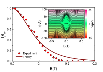
Owing to the large critical field of Nb a Josephson supercurrent is maintained up to relatively large magnetic fields. This is illustrated in Fig. 4 (inset), where the color-scaled voltage drop measured at sample H2 is given as a function of magnetic field and bias current. The measurement temperature was 0.4 K. The magnetic field was applied perpendicular to the substrate. The resulting values of normalized to the zero-field critical current are plotted as a function of in Fig. 4. A monotonous decrease of the measured critical current with magnetic field is found. A complete suppression of occurred at about 0.2 T. Earlier, a similar behavior of the critical current with magnetic field was observed in planar Nb/Au/Nb and Al/Au/Al Josephson junctions and in InN nanowire-based Josephson junctions.Frielinghaus et al. (2010) The monotonous decrease of with increasing can be explained within the framework of a recently developed theoretical model for the proximity effect in diffusive narrow-width Josephson junctions.Cuevas and Bergeret (2007); Bergeret and Cuevas (2008) There, it is shown that for junctions with a width comparable to or smaller than the magnetic length , the magnetic field acts as a pair-breaking factor that suppresses monotonously the proximity-induced superconductivity in the wire and the critical current.
For sample H2 the characteristic magnetic field defined by the flux quantum through the cross section of the normal wire, , is as large 0.13 T, resulting in nm. The value of is thus comparable to the junction width, so that the theoretical model for the limit of narrow-width Josephson junctions can be applied.Cuevas and Bergeret (2007); Bergeret and Cuevas (2008) We calculated the expected dependence of on using the Thouless energy defined by as a fitting parameter.Cuevas and Bergeret (2007); Bergeret and Cuevas (2008); Hammer et al. (2007) Here, is the diffusion constant and is the length of the junction. As can be seen in Fig. 4, a good agreement between experiment and theory is obtained. The best fit has been achieved for meV. This value is smaller than meV, determined from transport measurements in the normal state. We interpret the lower value of as compared to the Thouless energy obtained from the transport data by the presence of interface barriers in the junctions.Frielinghaus et al. (2010)
In Fig. 5(a) the differential resistance of sample L2 is plotted in color scale as a function of bias current and back-gate voltage. The measurements were taken at 0.4 K. It can be seen that on average the supercurrent range (black region) is reduced if a more negative gate voltage is applied. This is due to the corresponding decrease of the electron concentration in the nanowire. Since the current was biased from negative to positive values, the switching is nonsymmetric with respect to zero current, with the transition at negative and positive bias currents corresponding to the return current and the critical current , respectively. A closer look on Fig. 5(a) reveals that fluctuates as a function of back-gate voltage. The corresponding values of are plotted in Fig. 5(b). The average amplitude of the critical current fluctuations, i.e. the root-mean-square (rms) of fluctuations over the applied gate voltage range, is found to be nA. The critical current fluctuations were calculated by subtracting a linear increasing background current.
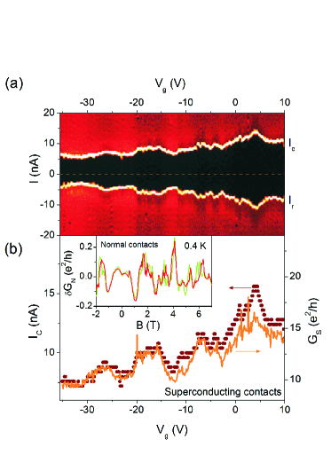
Mesoscopic fluctuations of the critical current have been theoretically studied mainly in two different regimes. For the short junction limit it is found that the fluctuations are universal and that the fluctuation amplitude depends only on the superconducting gap, : .Macêdo and Chalker (1994); Beenakker (1991); Beenakker and Rajaei (1994) The limit of long Josephson junctions, where the Thouless energy ETh is much smaller than the superconducting gap in the leads has been investigated by Altshuler and Spivak.Al’tshuler and Spivak (1987) In this model the energy scale for mesoscopic fluctuations in the critical current, , is set by the Thouless energy. Since in our case , we compared the experimental values of with the model of Alt’shuler and Spivak which is appropriate for this particular regime.Al’tshuler and Spivak (1987) Within this model the amplitude of supercurrent fluctuations at is given by . By taking a Thouless energy meV, as was estimated from the magnetic field dependence of for the sample L2, we obtain an expected fluctuation amplitude of nA. In the more recent model of Houzet and Skvortsov,Houzet and Skvortsov (2008) the proximity effect and the resulting formation of a minigap in the normal conductor is included in the analysis of the critical current fluctuations. For the long junction limit they obtained . According to this model we find an even higher expected fluctuation amplitude of approximately 18 nA. For both models the expected values of are considerably larger than the corresponding experimentally obtained values. The most probable reason of the lower measured value of is the presence of a non-ideal superconductor/normal conductor interface,Takayanagi et al. (1995b); Doh et al. (2005) i.e. an interface barrier or different Fermi velocities in both materials.Schäpers et al. (1997) Both contributions lead to a decrease of and can be expected to result in an according decrease of .
In Fig. 5(b) the normalized differential conductance is plotted in units of as a function of back-gate voltage. The conductance values have been taken at a bias voltage 0.1 mV, which is well below , so that multiple Andreev reflections partially contribute to the total conductance. However, we did not attempt to drive the junction into a higher bias state above or measure the fluctuations at temperatures above , such that any superconducting properties are suppressed. The reason is that under these conditions the quasi-equilibrium phase coherent transport regime is left. As can be seen in Fig. 5(b), the fluctuation pattern of follows almost perfectly the pattern of the previously discussed fluctuations in . A similar agreement between the fluctuation patterns of and has been observed before on Al/InAs-nanowire and on Nb/2-dimensional electron gas Josephson junctions.Doh et al. (2005); Takayanagi et al. (1995b)
The fluctuations in originate from the phase-coherent transport through a conductor with small dimensions where only a limited number of scattering centers are involved.Stone (1985); Al’tshuler (1985); Blömers et al. (2011) For our junction we find a fluctuation amplitude of , with calculated by subtracting the linearly increasing background conductance. In order to compare obtained for a sample with superconducting electrodes with the corresponding value of of a normal conducting reference sample, we have contacted a nanowire from the same growth run with normal Au/Ti electrodes. Here, the contact separation was 130 nm. As shown in Fig. 5(b) (inset), at a temperature of 0.4 K reproducible conductance fluctuations are measured as a function of magnetic field. However, the average conductance fluctuation amplitude of is significantly lower than the value found for the sample with superconducting electrodes. We attribute the enhanced conductance fluctuation observed for the sample with superconducting electrodes to the additional contribution of phase-coherent Andreev reflection. A similar behavior has been found in other Josephson junctions as well.Doh et al. (2005, 2008); Trbovic et al. (2010); Jespersen et al. (2009); Ojeda-Aristizabal et al. (2009) In Al-based Josephson junctions an enhancement of the average fluctuation amplitude between and has been reported,Trbovic et al. (2010) whereas in our Nb contacted junctions, we have found an enhancement by a factor of about 6. The larger enhancement compared to the values reported for Al-based junctions can be qualitatively explained by the larger superconducting energy gap of Nb compared to Al, resulting in a larger number of phase-coherent Andreev channels.
IV Summary and Conclusion
In summary, we have successfully fabricated and characterized Nb/InAs-nanowire/Nb Josephson junctions. By taking advantage of Nb as a superconductor, we could demonstrate that the junctions comprising a highly doped InAs nanowire show a clear Josephson supercurrent up to relatively high temperatures of 4 K. For the junctions with the lower doped nanowire, gate control of the Josephson supercurrent was achieved. The measurements of as a function of magnetic field show that a Josephson supercurrent can be maintained up to a field of 0.2 T. The observed monotonous decrease of with increasing magnetic field is explained by the magnetic pair breaking effect in narrow-width Josephson junctions.Cuevas and Bergeret (2007); Bergeret and Cuevas (2008) In the junctions with the lower doped nanowires the Josephson supercurrent as well as the conductance fluctuates when the gate voltage is varied. The measured average amplitude of supercurrent fluctuations was smaller than the theoretically expected value. The large difference between both values is attributed to the presence of a barrier at the Nb/nanowire interface. The average conductance fluctuation amplitude for the Nb/InAs-nanowire samples was considerably larger than the corresponding value for a reference sample with normal conducting Au/Ti contacts. We attribute this enhancement to the contribution of phase-coherent Andreev reflection.
IV.1 Acknowledgements
The authors are grateful to H. Kertz for assistance during the measurements and S. Trellenkamp for electron beam writing. H.Y.G. thanks The Scientific and Technological Research Council of Turkey (TUBITAK) foundation. I.E.B. acknowledges the Russian Foundation for Basic Research, Project No. RFBR 09-02-01499 for financial support.
References
- De Franceschi et al. (2010) S. De Franceschi, L. Kouwenhoven, C. Schönenberger, and W. Wernsdorfer, Nature Nano 5, 703 (2010).
- Schäpers (2001) T. Schäpers, Superconductor/Semiconductor Junctions, vol. 174 (Springer Tracts on Modern Physics, 2001).
- Akazaki et al. (1996) T. Akazaki, H. Takayanagi, J. Nitta, and T. Enoki, Appl. Phys. Lett. 68, 418 (1996).
- Takayanagi et al. (1995a) H. Takayanagi, T. Akazaki, and J. Nitta, Phys. Rev. Lett. 75, 3533 (1995a).
- Schäpers et al. (2003) Th. Schäpers, V. A. Guzenko, R. P. Müller, A. A. Golubov, A. Brinkman, G. Crecelius, A. Kaluza, and H. Lüth, Phys. Rev. B 67, 014522 (2003).
- Doh et al. (2005) Y.-J. Doh, J. A. van Dam, A. L. Roest, E. P. A. M. Bakkers, L. P. Kouwenhoven, and S. D. Franceschi, Science 309, 272 (2005).
- Xiang et al. (2006) J. Xiang, A. Vidan, M. Tinkham, R. M. Westervelt, and C. M. Lieber, Nature Nanotechnology 1, 208 (2006).
- van Dam et al. (2006) J. A. van Dam, Y. V. Nazarov, E. P. A. M. Bakkers, S. De Franceschi, and L. P. Kouwenhoven, Nature 442, 667 (2006).
- Frielinghaus et al. (2010) R. Frielinghaus, I. E. Batov, M. Weides, H. Kohlstedt, R. Calarco, and Th. Schäpers, Appl. Phys. Lett. 96, 132504 (2010).
- Roddaro et al. (2011) S. Roddaro, A. Pescaglini, D. Ercolani, L. Sorba, F. Giazotto, and F. Beltram, Nano Research 4, 259 (2011).
- Nishio et al. (2011) T. Nishio, T. Kozakai, S. Amaha, M. Larsson, H. A. Nilsson, H. Q. Xu, G. Zhang, K. Tateno, H. Takayanagi, and K. Ishibashi, Nanotechnology 22, 445701 (2011).
- Smit et al. (1989) K. Smit, L. Koenders, and W. Mönch, Journal of Vacuum Science & Technology B (Microelectronics Processing and Phenomena) 7, 888 (1989).
- Sand-Jespersen et al. (2007) T. Sand-Jespersen, J. Paaske, B. M. Andersen, K. Grove-Rasmussen, H. I. Jørgensen, M. Aagesen, C. B. Sørensen, P. E. Lindelof, K. Flensberg, and J. Nygård, Phys. Rev. Lett. 99, 126603 (2007).
- Hofstetter et al. (2009) L. Hofstetter, S. Csonka, J. Nygard, and C. Schönenberger, Nature 461, 960 (2009).
- Spathis et al. (2011) P. Spathis, S. Biswas, S. Roddaro, L. Sorba, F. Giazotto, and F. Beltram, Nanotechnology 22, 105201 (2011).
- Fasth et al. (2007) C. Fasth, A. Fuhrer, L. Samuelson, V. N. Golovach, and D. Loss, Phys. Rev. Lett. 98, 266801 (2007).
- Lutchyn et al. (2010) R. M. Lutchyn, J. D. Sau, and S. Das Sarma, Phys. Rev. Lett. 105, 077001 (2010).
- Cuevas and Bergeret (2007) J. C. Cuevas and F. S. Bergeret, Physical Review Letters 99, 217002 (pages 4) (2007).
- Bergeret and Cuevas (2008) F. S. Bergeret and J. C. Cuevas, J. Low Temp. Phys. 153, 304 (2008).
- Angers et al. (2008) L. Angers, F. Chiodi, G. Montambaux, M. Ferrier, S. Guéron, H. Bouchiat, and J. C. Cuevas, Physical Review B (Condensed Matter and Materials Physics) 77, 165408 (pages 12) (2008).
- Doh et al. (2008) Y.-J. Doh, S. D. Franceschi, E. P. A. M. Bakkers, and L. P. Kouwenhoven, Nano Letters 8, 4098 (2008).
- Jespersen et al. (2009) T. S. Jespersen, M. L. Polianski, C. B. S rensen, K. Flensberg, and J. Nyg rd, New Journal of Physics 11, 113025 (2009).
- Takayanagi et al. (1995b) H. Takayanagi, J. B. Hansen, and J. Nitta, Phys. Rev. Lett. 74, 166 (1995b).
- Wirths et al. (2011) S. Wirths, K. Weis, A. Winden, K. Sladek, C. Volk, S. Alagha, T. E. Weirich, M. von der Ahe, H. Hardtdegen, H. Lüth, et al., Journal of Applied Physics 110, 053709 (2011).
- Jarillo-Herrero et al. (2006) P. Jarillo-Herrero, J. van Dam, and L. Kouwenhoven, Nature 439, 953 (2006).
- Pallecchi et al. (2008) E. Pallecchi, M. Gaaß, D. A. Ryndyk, and C. Strunk, Applied Physics Letters 93, 072501 (2008).
- Courtois et al. (2008) H. Courtois, M. Meschke, J. T. Peltonen, and J. P. Pekola, Phys. Rev. Lett. 101, 067002 (2008).
- Octavio et al. (1983) M. Octavio, M. Tinkham, G. E. Blonder, and T. M. Klapwijk, Phys. Rev. B 27, 6739 (1983).
- Flensberg et al. (1988) K. Flensberg, J. B. Hansen, and M. Octavio, Phys. Rev. B 38, 8707 (1988).
- Cuevas et al. (2006) J. C. Cuevas, J. Hammer, J. Kopu, J. K. Viljas, and M. Eschrig, Phys. Rev. B 73, 184505 (2006).
- Blonder et al. (1982) G. E. Blonder, M. Tinkham, and T. M. Klapwijk, Phys. Rev. B 25, 4515 (1982).
- Batov et al. (2004) I. E. Batov, Th. Schäpers, A. A. Golubov, and A. V. Ustinov, Journal of Applied Physics 96, 3366 (2004).
- Chrestin et al. (1997) A. Chrestin, T. Matsuyama, and U. Merkt, Phys. Rev. B 55, 8457 (1997).
- Carbotte (1990) J. P. Carbotte, Rev. Mod. Phys. 62, 1027 (1990).
- Hammer et al. (2007) J. C. Hammer, J. C. Cuevas, F. S. Bergeret, and W. Belzig, Physical Review B 76, 064514 (2007).
- Macêdo and Chalker (1994) A. M. S. Macêdo and J. T. Chalker, Phys. Rev. B 49, 4695 (1994).
- Beenakker (1991) C. W. J. Beenakker, Phys. Rev. Lett 67, 3836 (1991).
- Beenakker and Rajaei (1994) C. W. J. Beenakker and B. Rajaei, Phys. Rev. B 49, 7499 (1994).
- Al’tshuler and Spivak (1987) B. Al’tshuler and B. Spivak, Zh. Eksp. Teo. Fiz. [Sov. Physics-JETP 65, 343-347 (1987)] 92, 609 (1987).
- Houzet and Skvortsov (2008) M. Houzet and M. A. Skvortsov, Phys. Rev. B 77, 024525 (2008).
- Schäpers et al. (1997) Th. Schäpers, A. Kaluza, K. Neurohr, J. Malindretos, G. Crecelius, A. van der Hart, H. Hardtdegen, and H. Lüth, Appl. Phys. Lett. 71, 3575 (1997).
- Stone (1985) A. D. Stone, Phys. Rev. Lett. 54, 2692 (1985).
- Al’tshuler (1985) B. Al’tshuler, Pis’ma Zh. Eksp. Teo. Fiz. [JETP Lett. 41, 648-651 (1985)] 41, 530 (1985).
- Blömers et al. (2011) C. Blömers, M. I. Lepsa, M. Luysberg, D. Grützmacher, H. Lüth, and Th. Schäpers, Nano Letters 11, 3550 (2011).
- Trbovic et al. (2010) J. Trbovic, N. Minder, F. Freitag, and C. Schönenberger, Nanotechnology 21, 274005 (2010).
- Ojeda-Aristizabal et al. (2009) C. Ojeda-Aristizabal, M. Ferrier, S. Guéron, and H. Bouchiat, Phys. Rev. B 79, 165436 (2009).