Dynamics and dissipation induced by single-electron tunneling in carbon nanotube nanoelectromechanical systems
Abstract
We demonstrate the effect of single-electron tunneling (SET) through a carbon nanotube quantum dot on its nanomechanical motion. We find that the frequency response and the dissipation of the nanoelectromechanical system (NEMS) to SET strongly depends on the electronic environment of the quantum dot, in particular on the total dot capacitance and the tunnel coupling to the metal contacts. Our findings suggest that one could achieve quality factors of 106 or higher by choosing appropriate gate dielectrics and/or by improving the tunnel coupling to the leads.
pacs:
81.07.Oj; 81.07.De; 85.85.+jCarbon nanotubes (CNT) have become an essential building block for nanoelectromechanical systems (NEMS). Their low mass and high Young’s modulus allow for instance ultrasensitive mass Lassagne et al. (2008); Chiu et al. (2008); Jensen et al. (2008) or force detection Eichler and et al. (2011); Lassagne et al. (2011) (electric and magnetic) over a wide range of frequencies and its small diameter enables even single-molecule detection Lassagne et al. (2011); Bogani and Wernsdorfer (2008); Urdampilleta et al. (2011). Moreover, CNT devices exhibit remarkable electronic transport properties, ranging from Kondo physics Nygård et al. (2000) to Coulomb blockade at high temperature Charlier et al. (2007). It was recently demonstrated that a CNT NEMS’ nanomechanical motion at very low temperature (i.e. in Coulomb blockade regime) is strongly affected by the electronic transport through the CNT quantum dot (QD), and vice versa: For instance, single-electron tunneling (SET) caused a frequency softening and increased dissipation when tuning the CNT dot’s potential through a Coulomb peak Lassagne and et al. (2009); Steele and et al. (2009); Hüttel et al. (2009).
Here we demonstrate that the response and dissipation of a CNT NEMS at very low temperature induced by zero bias SET through the CNT NEMS-QD critically depends on the dot capacitance, the tunnel coupling to the metal leads and temperature. We studied the frequency and dissipation response of nanomechanical bending modes to zero bias SET in suspended CNT devices with tunable tunnel couplings and different gate dielectrics, i.e. different dot capacitance. We observe that SET causes a frequency softening for small dot capacitance and/or tunnel coupling, whereas a frequency hardening or no frequency modulation is observed for large dot capacitance and/or tunnel coupling. We show that the dissipation of the CNT NEMS is mainly dominated by the capacitance, when electron tunneling through the dot is suppressed (i.e. in the Coulomb valley), whereas it is limited by the mean tunneling rate and the conductance, when electron tunneling through the dot is allowed (i.e. on a Coulomb peak). Finally we demonstrate that the tunnel current is the dominant dissipation mechanism in CNT NEMS at low temperature. Our findings are in fair agreement with a theoretical model provided previously Lassagne and et al. (2009); Steele and et al. (2009).
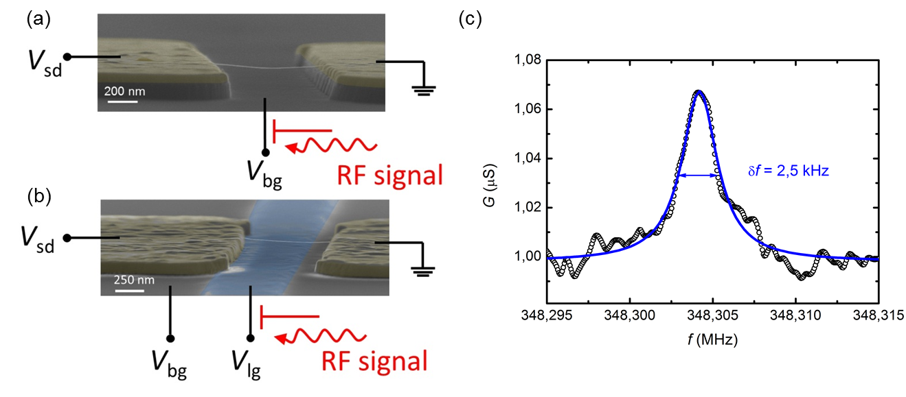
Low capacitance CNT quantum dots ( 20 - 40 aF) were obtained by using silicon dioxide as gate dielectric [Fig. 1(a)]. First, source-drain electrodes are patterned by optical DUV lithography and e-beam evaporation of Mo (20 nm) and Pt (160 nm) on 500 nm of thermal SiO2. To ensure the suspension of the CNT, 150 nm of SiO2 are dry etched in CHF3 plasma. High capacitance CNT quantum dots ( 160 - 260 aF) are obtained with high- gate dielectrics Al2O3 [Fig. 1(b)]. First, a 1 m-wide metallic local gate is patterned by optical DUV lithography and e-beam evaporation of Mo (20 nm) on 300 nm of thermal SiO2. A layer of 100 nm of Al2O3 is then deposited by atomic layer deposition. Using optical DUV lithography and e-beam evaporation of Mo (20 nm) and Pt (160 nm), source-drain electrodes are aligned above the local gate. Suspended CNT’s are finally grown by chemical vapor deposition at 800∘C from a CH4 feedstock and Fe/Mo catalyst spots patterned on the source-drain electrodes next to the junction. The CNT device length is approximately 800 nm ( 50 nm) and the dot capacitances are deduced from the dot’s charging energy at low temperature. The spread in capacitance values of nominally identically fabricated devices is due to variations in the nanotubes length and slack (see Supporting Information).
The measurements are carried out in a 3He/4He dilution refrigerator with a base temperature of 30 mK. The NEMS actuation and detection scheme used in our experiment is similar to the one used by Steele and co-workers Steele and et al. (2009); Hüttel et al. (2009). The RF actuation signal is injected into the gate electrode via a home-built bias T. As the induced mechanical motion changes the charge flow through the CNT quantum dot and vice versa, we can detect the CNT resonance through a change in zero bias conductance. The actuation power is kept to a minimum ( -100 dBm) in order to ensure a quasi-linear regime of the oscillator and a high lorentzian resonance shape [Fig. 1(c)]. All measurements were done under zero bias with a standard lock-in technique.
SET in a CNT NEMS-QD can be considered as an external perturbation to the CNT mechanical motion, and vice versa. This perturbation can be described as an electrodynamic force acting on the CNT. The contribution of this force, which is in phase with the mechanical motion, is responsible for a frequency modulation , whereas a contribution of the force being out of phase with mechanical motion induces a modification of the dissipation and the quality factor . and can be expressed as follows Lassagne and et al. (2009)
| (1) | |||||
| (2) |
Where is the mean tunnel coupling of the dot to the leads, yielding , and is the total dot capacitance. We can estimate the tunnel coupling for each device from the line shape of the Coulomb blockade peaks (see Supporting Information). Eqs. (1) and (2) are valid in the regime of Coulomb blockade and if .
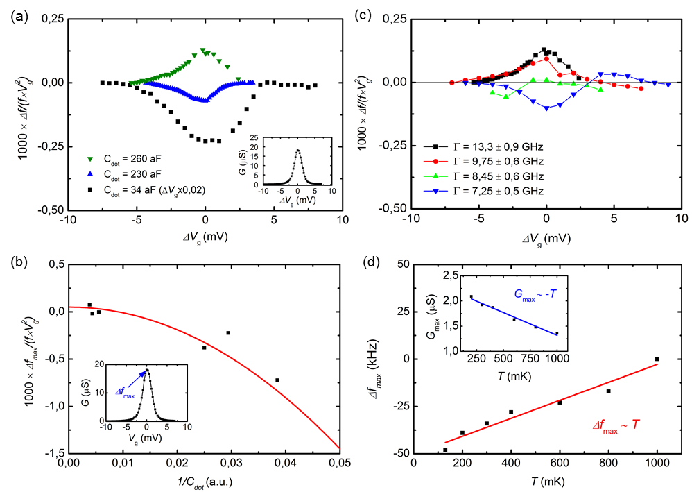
First, we compare the frequency response (scaled with ) of devices with different dot capacitances . We studied the frequency response for comparable Coulomb peaks height, i.e. for comparable conductance 20 S. The tunnel coupling are on the order of 10 GHz. As depicted in Fig. 2(a), we observe a strong frequency softening for small dot capacitances, whereas for high dot capacitances a frequency hardening or no modulation is observed. As shown in Fig. 2(b), the experimental data are in fair agreement with the model. A fit with Eq. 1 yields fitting parameters = 8 10 F2/Nm and 10 GHz, which are in rather good agreement with previous experiments Lassagne and et al. (2009); Steele and et al. (2009); Sazonova et al. (2004). Fig. 2(c) shows the (scaled) frequency modulation for different Coulomb peaks and tunneling rates on a given device (device 1). It was shown previously that one can tune a CNT quantum dot from a Coulomb blockade regime to a regime of strong tunnel coupling by simply changing the CNT’s gate potential Jespersen et al. (2011); Steele et al. (2009). Hence, we can change the tunnel coupling by tuning the gate voltage of our CNT device and estimate the values of from the Coulomb peak line shape (see Supporting Information). The dot capacitance = 260 aF remain unchanged by tuning the gate voltage. As increases, the CNT becomes stiffer, resulting in a sign change of and the transition from a frequency softening to frequency hardening, in qualitative agreement with Eq. 1 [Fig. 2(c)].
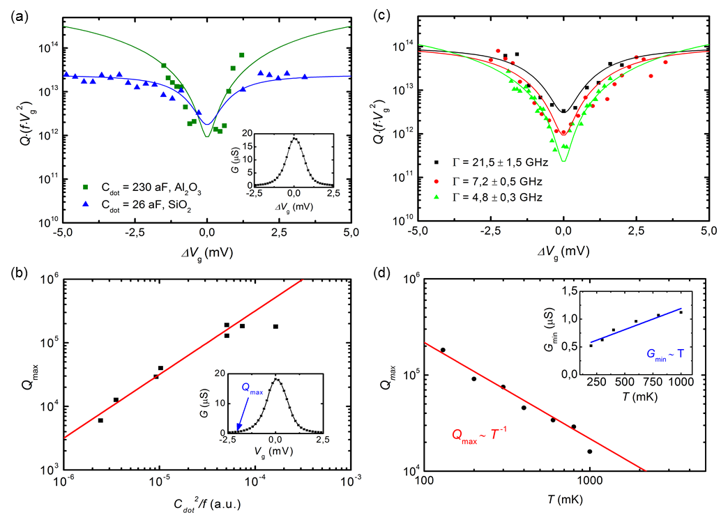
Fig. 3(a) depicts the effect of SET on the dissipation of the CNT NEMS, i.e. the factor (scaled with ), for devices with different dot capacitances. From Eq. 2, we expect an increase of the Q factor with increasing capacitance in the limit of suppressed SET through the dot. Indeed, in a region of suppressed SET (),the factor is larger for devices with higher dot capacitance [Fig. 3(a)]. The tunnel coupling GHz and the conductance 18 S are comparable for both traces. Fig. 3(b) shows the factor (scaled with ) in the limit of suppressed SET () as a function of the dot capacitance for all measured devices. The fit with Eq. 2 yields = 1 10 F2/Nm and 10 GHz which is consistent with the fitting parameters of Fig. 2(b) and previous experiments Lassagne and et al. (2009); Steele and et al. (2009); Sazonova et al. (2004). Despite the good agreement between theory and experiment, we observe deviations from the model for some devices in Fig. 2(b) and 3(b), which we attribute to variations in (see Supporting Information). Moreover, we expect from Eq. 2 and previous experiments Lassagne and et al. (2009); Steele and et al. (2009) an enhanced electromechanical dissipation in a given device if the conductance (i.e. the tunnel current) and the tunnel resistance at the nanotube-electrode interface are increased, in analogy to the current dissipation in a simple resistance. Indeed we observe increased dissipation (decreased Q factor) when tuning the gate voltage through a Coulomb peak [Fig. 3(a) and 3(c)]. In Fig 3(c) (device 2), this effect becomes more pronouced as we move to gate voltage regions with a smaller tunneling rate , i.e. larger tunnel resistance at the nanotube-electrode interface. The dot capacitance yields 160 aF for this device and the height of the Coulomb peak are comparable for all traces ( 7 S). Therefore, the CNT capacitance is the limiting factor for the dissipation in regions of suppressed SET, whereas the mean tunnel coupling and the tunneling current itself define the dissipation in regions of strong SET. We conclude that the electron transport through the CNT is the main dissipation mechanism in our nanoelectromechanical system.
Finally we study the temperature dependance of the frequency response and the dissipation. Fig. 2(d) depicts the frequency shift for whereas Fig. 3(d) shows the quality factor for as function of temperature. A fit of the data yields and . As temperature increases the Coulomb blockade peak broadens and becomes smaller (see supporting information Fig. S3). As a result decreases whereas increases with temperature, as depicted in the insets of Figs. 2(d) and 3(d). From the data fit we obtain and . It was previously demonstrated that carbon nanotubes show Luttinger liquid behavior Bockrath and et al. (1999); Kane et al. (1997); Egger and Gogolin (1997), where the conductance follows a characteristic power law dependence as a function of temperature , being related to the Luttinger parameter g by Bockrath and et al. (1999); Kane et al. (1997). We find and a Luttinger parameter of , which is close to previous measurements Bockrath and et al. (1999) and theoretical predictions Kane et al. (1997); Egger and Gogolin (1997). Comparing the temperature dependance of the conductance, the quality factor and the frequency shift we finally obtain and , which is in full agreement with Eqs. 1 and 2. We can conclude that the current is the dominant dissipation mechanism for carbon nanotube based NEMS in a Coulomb blockade regime at cryogenic temperatures.
We have demonstrated that the response and the dissipation to single-electron tunneling of carbon nanotube NEMS at low temperature depends on the dot capacitance and the tunnel coupling to the leads, the tunnel current itself being the main dissipation mechanism in the system. By choosing high- dielectrics (HfO2 or ZrO2) and improving the tunnel contact to the metal leads, one could significantly enhance the quality factor to values exceeding 106. It was proposed in theoretical calculation that one can use such high CNT NEMS as magnetic torque or force detectors for nanoparticles Lassagne et al. (2011) or single molecule magnets Kovalev et al. (2011); Garanin and Chudnovsky (2011) grafted to the CNT NEMS. In principle one can achieve a sensitivity of one at low temperature, whereas the best magnetometers, for instance the micro-SQUID, only have a sensitivity of 103 Wernsdorfer (2009). Finally, such molecular quantum spintronic device would allow single spin manipulation on a molecular level.
Acknowledgements.
This work is partially supported by the ANR-PNANO project MolNanoSpin No. ANR-08-NANO-002 and ERC Advanced Grant MolNanoSpin No. 226558. M.G. acknowledges the financial support from the RTRA Nanosciences Foundation. Samples were fabricated in the NANOFAB facility of the Neel Institute. We thank F. Balestro, E. Bonet, T. Crozes, J.P. Cleuziou, E. Eyraud, T. Fournier, R. Haettel, C. Hoarau, D. Lepoittevin, V. Nguyen, V. Reita, A. Reserbat-Plantey, C. Thirion, M. Urdampilleta.References
- Lassagne et al. (2008) B. Lassagne, D. Garcia-Sanchez, A. Aguasca, and A. Bachtold, Nano Lett. 8, 3735 (2008).
- Chiu et al. (2008) H.-Y. Chiu, P. Hung, H. W. C. Postma, and M. Bockrath, Nano Lett. 8, 4342 (2008).
- Jensen et al. (2008) K. Jensen, K. Kim, and A. Zettl, Nature Nanotech. 3, 533 (2008).
- Eichler and et al. (2011) A. Eichler et al., Nature Nanotech. 6, 339 (2011).
- Lassagne et al. (2011) B. Lassagne, D. Ugnati, and M. Respaud, Phys. Rev. Lett. 107, 130801 (2011).
- Bogani and Wernsdorfer (2008) L. Bogani and W. Wernsdorfer, Nature Mater. 7, 179 (2008).
- Urdampilleta et al. (2011) M. Urdampilleta, S. Klyatskaya, J.-P. Cleuziou, M. Ruben, and W. Wernsdorfer, Nature Mater. 10, 502 (2011).
- Nygård et al. (2000) J. Nygård, D. H. Cobden, and P. E. Lindelof, Nature (London) 408, 342 (2000).
- Charlier et al. (2007) J.-C. Charlier, X. Blase, and S. Roche, Rev. Mod. Phys. 79, 677 (2007).
- Lassagne and et al. (2009) B. Lassagne et al., Science 325, 1107 (2009).
- Steele and et al. (2009) G. A. Steele et al., Science 325, 1103 (2009).
- Hüttel et al. (2009) A. K. Hüttel et al., Nano Lett. 9, 2547 (2009).
- Sazonova et al. (2004) V. Sazonova et al., Nature (London) 431, 284 (2004).
- Jespersen et al. (2011) T. Jespersen et al., Nature Phys. 7, 348 (2011).
- Steele et al. (2009) G. A. Steele, G. Gotz, and L. P. Kouwenhoven, Nature Nanotech. 4, 363 (2009).
- Bockrath and et al. (1999) M. Bockrath et al., Nature (London) 397, 598 (1999).
- Kane et al. (1997) C. Kane, L. Balents, and M. Fisher, Phys. Rev. Lett. 79, 5086 (1997).
- Egger and Gogolin (1997) R. Egger and A. Gogolin, Phys. Rev. Lett. 79, 5082 (1997).
- Kovalev et al. (2011) A. A. Kovalev, L. X. Hayden, G. E. W. Bauer, and Y. Tserkovnyak, Phys. Rev. Lett. 106, 147203 (2011).
- Garanin and Chudnovsky (2011) D. Garanin and E. Chudnovsky, Phys. Rev. X 1, 011005 (2011).
- Wernsdorfer (2009) W. Wernsdorfer, Supercond. Sci. Technol. 22, 064013 (2009).
*
See pages 1 of Dynamics_and_dissipation_SI.pdf See pages 2 of Dynamics_and_dissipation_SI.pdf See pages 3 of Dynamics_and_dissipation_SI.pdf See pages 4 of Dynamics_and_dissipation_SI.pdf See pages 5 of Dynamics_and_dissipation_SI.pdf See pages 6 of Dynamics_and_dissipation_SI.pdf See pages 7 of Dynamics_and_dissipation_SI.pdf