Local Gating of an Ir(111) Surface Resonance by Graphene Islands
Abstract
The influence of graphene islands on the electronic structure of the Ir(111) surface is investigated. Scanning tunneling spectroscopy (STS) indicates the presence of a two-dimensional electron gas with a binding energy of and an effective mass of underneath single-layer graphene on the Ir(111) surface. Density functional calculations reveal that the STS features are predominantly due to a holelike surface resonance of the Ir(111) substrate. Nanometer-sized graphene islands act as local gates, which shift and confine the surface resonance.
pacs:
73.20.At, 73.21.Fg, 73.22.PrOn a number of metal surfaces, single layers of graphene may be grown. Owing to their different graphene–metal interactions Wintterlin and Bocquet (2009), these substrates may modify the electronic structure of the graphene layer. For example, the and bands of graphene, which give rise to a Dirac cone dispersion in the pristine material, are significantly altered on Ni(111) and Ru(0001) Nagashima et al. (1994); Himpsel et al. (1982), where a gap in the Dirac bands opens. In contrast, from Ir(111), an almost unchanged band structure of graphene has been reported Pletikosić et al. (2009). The modification of the electronic structure of the substrate upon graphene adsorption has hardly been investigated. From calculations, quenching of the Ni(111) surface state upon graphene adsorption was predicted Dzemiantsova et al. (2011). The only experiment related to this issue addressed a spatial variation of the Ru(0001) states, which arises from a graphene-induced moiré pattern Gyamfi et al. (2011). This state of affairs is surprising as electronic states at surfaces are sensitive probes of the interaction with adsorbates.
Here, we combine scanning tunneling spectroscopy and density functional theory (DFT) calculations of Ir(111) covered with a single layer of graphene. Spectra of the differential conductance (; : current; : sample voltage) of pristine and graphene-covered Ir(111) reveal a holelike surface resonance. Intriguingly, the most prominent features in the spectra are due to this resonance at the Ir–graphene interface rather than to any states of the graphene layer. This effect is attributed to the selectivity of the tunneling current for states with small parallel momentum. Although the electronic structure of graphene is only weakly perturbed by the Ir(111) substrate, graphene shifts the Ir surface resonance by towards the Fermi level. As a result, graphene islands act as local gates which confine the surface resonance and induce characteristic standing wave patterns. The resonance shift and an effective mass (: free electron mass) determined from these patterns are consistent with DFT results.
Experiments were performed with a home-built scanning tunneling microscope (STM), operated at in an ultrahigh vacuum. Ir(111) surfaces were cleaned by cycles of Ar+ bombardment and annealing. Graphene films were grown by exposing the sample to of at room temperature and subsequent annealing at . This procedure leads to a partial coverage of Ir(111) by highly ordered graphene N’Diaye et al. (2006). Au tips were prepared by ex-situ cutting, in-vacuo heating and Ar+ bombardment. Spectra of were acquired by a standard lock-in technique (modulation frequency: 9.1 kHz, modulation amplitude: 10 mV) and subsequently normalized by to compensate for the voltage-dependent transmission of the tunneling barrier Feenstra et al. (1987).
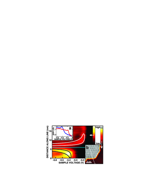
Figure 1 shows normalized data, which were obtained along a slightly curved line [Inset (b) to Fig. 1] crossing a step from bare Ir onto a graphene island. Above the bare Ir(111) surface, a steplike decrease in the signal at [Inset (a) to Fig. 1, blue (black) line] occurs, which is indicative of a holelike surface state or resonance 111The large width of the onset is consistent with the fact that the resonance is degenerate with bulk states. It may also be affected by residual adsorbates on Ir(111), which attenuate the signal of the surface resonance in their vicinity. Hence, spectra were obtained as far away from such defects as possible.. Such a resonance was previously observed with photoelectron spectroscopy van der Veen et al. (1980); Pletikosić et al. (2010). Above the graphene layer, the steplike feature is shifted to [Inset (a) to Fig. 1, red (dark gray) line]. When approaching the edge of the graphene island from either side, the step moves towards lower voltages and disappears on top of the graphene edge. This spatial variation of the shift can be explained by scattering at the graphene edge. The rather strong interaction between graphene edges and the Ir(111) substrate bends the graphene edges towards the metal and leads to the formation of chemical bonds between Ir and C atoms at the island edge Lacovig et al. (2009). The Ir(111) surface resonance is considered as a free electron gas with a binding energy and effective mass scattered from a hard-wall potential provided by the graphene edges. The spatial variation of the local density of states (LDOS), , can then be described as
| (1) |
where is the zeroth-order Bessel function, is the parallel momentum, is the energy, and is the position of the hard-wall potential Avouris et al. (1994); Davis et al. (1991); Crommie et al. (1993). Lines in Fig. 1 show contours of constant LDOS calculated for (see confinement analysis below), (curved black line) and (curved white line), for Ir(111) and graphene-covered Ir(111), respectively. To match experimental data, a Gaussian broadening of was applied. Further, the energies and were chosen to yield a good fit between the calculated first maximum of the oscillation (embraced by contour lines) and the experimental data. The simple hard-wall model reproduces the curvature and position of the LDOS maxima quite well and yields an energetic shift of the surface resonance between bare and graphene-covered Ir of . The energies fit well to the energies extracted from the single spectra; also matches the energy obtained by confinement analysis (see below). It is important to note that the data do not reveal any particle-hole symmetric counterpart of these confinement features above the Fermi level. At energies below (not shown in Fig. 1) variations in the LDOS with the periodicity of the moiré pattern predominate, probably due to weak periodic potential modulations.
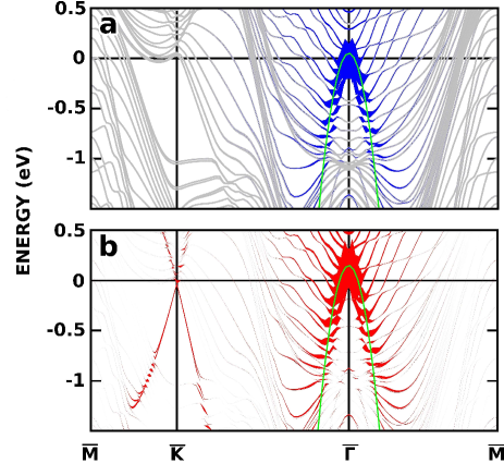
To further support the above model, DFT calculations of the pristine and graphene-covered Ir(111) surface were performed 222The Ir surface was modeled using a slab of 18 layers of Ir atoms and a vacuum gap of . A -mesh of points and a kinetic energy cut-off of were used. To study graphene on Ir(111), the slab was covered with graphene on one side with one of the two C atoms of the graphene unit cell on top of an Ir atom and the graphene lattice constant adjusted to match the Ir lattice. Spin-orbit coupling was taken into account to correctly model splitting of surface states Pletikosić et al. (2010).. We used the projector-augmented plane wave method Blöchl (1994); Kresse and Joubert (1999), as implemented in the Vienna ab initio simulation package Kresse and Hafner (1994). Light gray lines in Fig. 2(a) show the calculated band structure of an Ir(111) surface. Near the Fermi energy of the Ir(111) system, various bands originate from bulk bands with or character and there are several surface states around the bulk band gap near and a surface resonance near . This resonance is mainly derived from Ir orbitals of the first few atomic layers near the surface. In the energy range probed in the STM experiments, the calculated dispersion of the surface resonance is approximately parabolic, with an effective mass of [Fig. 2(a), green (gray) line]. At the graphene-covered surface [Fig. 2(b)], two additional bands derived from the C orbitals occur and form a Dirac cone near in agreement with previous photoemission Pletikosić et al. (2010) and DFT Pletikosić et al. (2009) studies. On the graphene-covered surface, the resonance is shifted upwards [Fig. 2(b), green (gray) line] by an amount which depends on the distance between the graphene sheet and the topmost Ir layer. For typical spacings between and Busse et al. (2011), the calculated shift is between and , which is consistent with our experimental value of .
To trace back the origin of the resonance shift upon graphene adsorption, calculations were performed in which the graphene C atoms were replaced by chemically fully inert Ne atoms. As a result, a Ne layer shifts the Ir surface resonance upwards by virtually the same amount as the graphene layer. As Ne provides no states at the Fermi level which could donate or accept charge from the Ir surface, the upward shift of the resonance is most likely due to a significant Pauli repulsion. Nevertheless, Coulomb potential effects, e. g., via charge redistribution Busse et al. (2011), occur and cannot be disregarded in modeling the full electronic structure of graphene/Ir(111). The calculations further show a downward shift of the Dirac cone when the graphene sheet is pushed towards the Ir substrate. This shift cannot be explained by Pauli repulsion and demonstrates that Coulomb potential effects are predominant for the energy of the graphene Dirac point.
To determine the contributions of the various states to the tunneling current, the approach of Tersoff and Hamann Tersoff and Hamann (1983); *art:Tersoff2 was used and the tip was modeled as an orbital . Based on an estimate of the experimental tip–sample distance fno the orbital is placed above the surface. The overlap , where is the wave function of a band at wave vector , is indicated by the width of the colored bands in Fig. 2. On both surfaces, clean and graphene-covered Ir(111), the main contribution to the current is due to the aforementioned surface resonance. The current due to the Dirac bands of graphene is significantly smaller. This may be understood from the parallel momenta of these states, which affect their decay into vacuum. The surface resonance is located around and thus decays less rapidly than the Dirac cone states near 333The periodic potential associated with the moiré superlattice of graphene on Ir(111), which is not included in the calculations, may in principle scatter states from to the center of the Brillouin zone. However, owing to the large lattice constant of the superstructure, the associated momentum is small and multiple scattering steps are required, which makes this mechanism unlikely.. Therefore, the steps in the spectra may safely be attributed to the (shifted) Ir(111) surface resonance. This result is also in agreement with the absence of electron–hole symmetry from the experimental spectra. In recent publications Hämäläinen et al. (2011); Phark et al. (2011), scanning tunneling spectroscopy data from graphene on Ir(111) are attributed to tunneling from graphene states. However, the analyses of Refs. Hämäläinen et al., 2011; Phark et al., 2011 neglect the substrate electronic states at the Brillouin zone center. In contrast, the present results show the importance of substrate states at which give the dominant contribution to the current in our STM experiments.
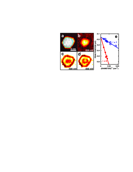
In addition to scattering at their edges, graphene islands lead to confinement of the hole states. Figure 3 shows an STM image of a graphene island along with normalized maps recorded at constant current. At increasingly negative sample bias [Figs. 3(b)–(d)] the pattern inside the island evolves from a central maximum over a ring to a ring with a central maximum, as expected for confined states with zero, one, and two nodes, respectively. For a more detailed analysis, we model the island by a circular quantum dot with hard walls. The eigenenergies of a confined electron gas are Platt (1954)
| (2) |
where is the th root of the th-order Bessel function and is the island diameter. Figure 3(e) displays the energies of the first two resonances which exhibit an LDOS maximum at the island center ( and ) evaluated from spatially resolved spectra of 8 nearly circular islands with diameters between and . The effective island diameters were determined from an inscribed circle, which touches the island boundaries at the midpoint of the step edge [Fig. 3(a), blue (light gray) line]. Energies calculated according to Eq. (2) with and [Fig. 3(e), lines] match the experimental data very well.
As a final test of the model spatially resolved spectra from a roundish island are compared with the calculated LDOS. The LDOS, , of the surface resonance confined to a disk is
| (3) |
are solutions to the Schrödinger equation as described by Platt et al. Platt (1954),
| (4) |
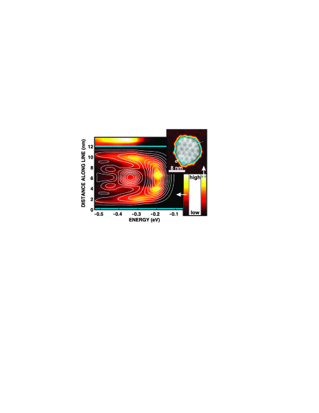
is a Gaussian broadening reflecting a finite lifetime of the states. While the broadening may depend on energy Jensen et al. (2005), the constant broadening assumed here is sufficient to match the experimental observations. Figure 4 shows a series of 29 normalized spectra measured along a line across a graphene island (inset). Light gray contour lines show the calculated LDOS using the measured diameter of (blue (gray) horizontal lines). The qualitative agreement of the theoretical and experimental data is further evidence that graphene islands confine the Ir(111) resonance.
In conclusion, van der Waals-bonded graphene on Ir(111) induces a pronounced shift in the Ir(111) surface resonance. The disappearance of the resonance at graphene edges indicates the covalent carbon-metal interaction, which acts as a hard-wall potential for scattering of resonance electrons. Nanometer-sized graphene flakes can therefore confine quasi-two-dimensional electron gases to artificial quantum dots.
Funding by the Deutsche Forschungsgemeinschaft via SPP 1459 and SFB 668, and the Schleswig-Holstein-Fonds, as well as computer time at HLRN, are acknowledged.
Note added in proof: Results concerning confined electronic states in graphene islands on Ir(111) Subramaniam et al. (2012) have been published after submission of this manuscript. Ref. Subramaniam et al., 2012 attributes the confined states to either graphene states or the scattered Ir(111) surface resonance, depending on the graphene island size. This is in contrast to our interpretation that the surface resonance predominates the STM data for any island size.
During the refereeing process an experimental observation of a graphene-induced shift of the Ir(111) surface resonance has been reported Varykhalov et al. (2012).
References
- Wintterlin and Bocquet (2009) J. Wintterlin and M.-L. Bocquet, Surf. Sci. 603, 1841 (2009).
- Nagashima et al. (1994) A. Nagashima, N. Tejima, and C. Oshima, Phys. Rev. B 50, 17487 (1994).
- Himpsel et al. (1982) F. Himpsel, K. Christmann, P. Heimann, D. Eastman, and P. J. Feibelman, Surf. Sci. 115, L159 (1982).
- Pletikosić et al. (2009) I. Pletikosić, M. Kralj, P. Pervan, R. Brako, J. Coraux, A. T. N’Diaye, C. Busse, and T. Michely, Phys. Rev. Lett. 102, 056808 (2009).
- Dzemiantsova et al. (2011) L. V. Dzemiantsova, M. Karolak, F. Lofink, A. Kubetzka, B. Sachs, K. von Bergmann, S. Hankemeier, T. O. Wehling, R. Frömter, H. P. Oepen, A. I. Lichtenstein, and R. Wiesendanger, Phys. Rev. B 84, 205431 (2011).
- Gyamfi et al. (2011) M. Gyamfi, T. Eelbo, M. Waśniowska, and R. Wiesendanger, Phys. Rev. B 83, 153418 (2011).
- N’Diaye et al. (2006) A. T. N’Diaye, S. Bleikamp, P. J. Feibelman, and T. Michely, Phys. Rev. Lett. 97, 215501 (2006).
- Feenstra et al. (1987) R. Feenstra, J. A. Stroscio, and A. Fein, Surf. Sci. 181, 295 (1987).
- Note (1) The large width of the onset is consistent with the fact that the resonance is degenerate with bulk states. It may also be affected by residual adsorbates on Ir(111), which attenuate the signal of the surface resonance in their vicinity. Hence, spectra were obtained as far away from such defects as possible.
- van der Veen et al. (1980) J. F. van der Veen, F. J. Himpsel, and D. E. Eastman, Phys. Rev. B 22, 4226 (1980).
- Pletikosić et al. (2010) I. Pletikosić, M. Kralj, D. Šokčević, R. Brako, P. Lazić, and P. Pervan, J. Phys.: Condens. Matter 22, 135006 (2010).
- Lacovig et al. (2009) P. Lacovig, M. Pozzo, D. Alfè, P. Vilmercati, A. Baraldi, and S. Lizzit, Phys. Rev. Lett. 103, 166101 (2009).
- Avouris et al. (1994) Ph. Avouris, I.-W. Lyo, R. E. Walkup, and Y. Hasegawa, J. Vac. Sci. Technol. B 12, 1447 (1994).
- Davis et al. (1991) L. C. Davis, M. P. Everson, R. C. Jaklevic, and W. Shen, Phys. Rev. B 43, 3821 (1991).
- Crommie et al. (1993) M. F. Crommie, C. P. Lutz, and D. M. Eigler, Nature 363, 524 (1993).
- Note (2) The Ir surface was modeled using a slab of 18 layers of Ir atoms and a vacuum gap of . A -mesh of points and a kinetic energy cut-off of were used. To study graphene on Ir(111), the slab was covered with graphene on one side with one of the two C atoms of the graphene unit cell on top of an Ir atom and the graphene lattice constant adjusted to match the Ir lattice. Spin-orbit coupling was taken into account to correctly model splitting of surface states Pletikosić et al. (2010).
- Blöchl (1994) P. Blöchl, Phys. Rev. B 50, 17953 (1994).
- Kresse and Joubert (1999) G. Kresse and D. Joubert, Phys. Rev. B 59, 1758 (1999).
- Kresse and Hafner (1994) G. Kresse and J. Hafner, J. Phys.: Condens. Matter 6, 8245 (1994).
- Busse et al. (2011) C. Busse, P. Lazić, R. Djemour, J. Coraux, T. Gerber, N. Atodiresei, V. Caciuc, R. Brako, A. N’Diaye, S. Blügel, J. Zegenhagen, and T. Michely, Phys. Rev. Lett. 107, 036101 (2011).
- Tersoff and Hamann (1983) J. Tersoff and D. R. Hamann, Phys. Rev. Lett. 50, 1998 (1983).
- Tersoff and Hamann (1985) J. Tersoff and D. R. Hamann, Phys. Rev. B 31, 805 (1985).
- (23) To estimate the tip-sample distance the tip was approached to the surface and the current was simultaneously measured. A drastic deviation of from an exponential signals the formation of a contact Limot et al. (2005); Altenburg et al. (2010). Assuming a typical bond length of at contact, we find at typical tunneling conditions.
- Note (3) The periodic potential associated with the moiré superlattice of graphene on Ir(111), which is not included in the calculations, may in principle scatter states from to the center of the Brillouin zone. However, owing to the large lattice constant of the superstructure, the associated momentum is small and multiple scattering steps are required, which makes this mechanism unlikely.
- Hämäläinen et al. (2011) S. K. Hämäläinen, Z. Sun, M. P. Boneschanscher, A. Uppstu, M. Ijäs, A. Harju, D. Vanmaekelbergh, and P. Liljeroth, Phys. Rev. Lett. 107, 236803 (2011).
- Phark et al. (2011) S.-h. Phark, J. Borme, A. L. Vanegas, M. Corbetta, D. Sander, and J. Kirschner, ACS Nano 5, 8162 (2011), http://pubs.acs.org/doi/pdf/10.1021/nn2028105 .
- Platt (1954) J. R. Platt, J. Chem. Phys. 22, 1448 (1954).
- Jensen et al. (2005) H. Jensen, J. Kröger, R. Berndt, and S. Crampin, Phys. Rev. B 71, 155417 (2005).
- Subramaniam et al. (2012) D. Subramaniam, F. Libisch, Y. Li, C. Pauly, V. Geringer, R. Reiter, T. Mashoff, M. Liebmann, J. Burgdörfer, C. Busse, T. Michely, R. Mazzarello, M. Pratzer, and M. Morgenstern, Phys. Rev. Lett. 108, 046801 (2012).
- Varykhalov et al. (2012) A. Varykhalov, D. Marchenko, M. R. Scholz, E. D. L. Rienks, T. K. Kim, G. Bihlmayer, J. Sánchez-Barriga, and O. Rader, Phys. Rev. Lett. 108, 066804 (2012).
- Limot et al. (2005) L. Limot, J. Kröger, R. Berndt, A. Garcia-Lekue, and W. A. Hofer, Phys. Rev. Lett. 94, 126102 (2005).
- Altenburg et al. (2010) S. J. Altenburg, J. Kröger, B. Wang, M.-L. Bocquet, N. Lorente, and R. Berndt, Phys. Rev. Lett. 105, 236101 (2010).