Manifestation of the shape and edge effects in spin-resolved transport through graphene quantum dots
Abstract
We report on theoretical studies of transport through graphene quantum dots weakly coupled to external ferromagnetic leads. The calculations are performed by exact diagonalization of a tight-binding Hamiltonian with finite Coulomb correlations for graphene sheet and by using the real-time diagrammatic technique in the sequential and cotunneling regimes. The emphasis is put on the role of graphene flake shape and spontaneous edge magnetization in transport characteristics, such as the differential conductance, tunneling magnetoresistance (TMR) and the shot noise. It is shown that for certain shapes of the graphene dots a negative differential conductance and nontrivial behavior of the TMR effect can occur.
pacs:
73.63.Kv, 73.23.Hk, 73.22.Pr, 85.75.-dI Introduction
Since its discovery, novoselov2004 graphene has been attracting an increasing attention due to its exceptional physical properties and also possibilities of various promising practical applications. Geim2007 ; katsnelson ; castro For example, owing to a very long spin diffusion length observed in graphene, tombros07 one may expect that graphene will play an important role in future molecular spintronics. Moreover, with the advent of new powerful experimental techniques, it is possible now to engineer and fabricate graphene structures of various shapes and sizes, ranging from sheets of large area to extremely small graphene flakes. The latter can in particular exhibit single-electron charging effects and, thus, behave as typical quantum dots - similar to quantum dots based on two-dimensional electron gas. sols07 ; ponomarenko08 ; stampfer08 ; todd09
In such small graphene flakes, the role of edges is much increased in comparison to large graphene sheets. It is also well known on theoretical grounds that zigzag edges of graphene nanostructures have large densities of states, which in the presence of strong enough on-site Coulomb repulsions can result in the appearance of edge magnetism. Fujita96 ; Yazyev10 ; Acik11 Indeed, it has been confirmed experimentally by scanning tunneling spectroscopy measurements that graphene nanoribbons and quantum dots reveal highly enhanced densities of states (DOS) at the zigzag-type fragments of their edges. Klusek00 ; Kobayashi05 It is worth noting, that the problem of graphene/graphite’s edges has been recently under intensive studies, as the carbon-based nanostructures can potentially be used in modern nanoelectronics, including also spintronics. Sutter09 ; Son06 ; Kim08 ; Munoz-Rojas09 ; SK09 ; Zhou10 ; Han11 ; Weymann08 Very recently, it has been demonstrated experimentally that the edge DOSs in graphene nanostructures are spin-split. Tao11 Following this line, in an attempt to gain additional insights into the edge states, we suggest another approach to the problem, namely a visualization of the effect of magnetic edges by the analysis of Coulomb blockade spectra for graphene dots of different geometries. To reach this objective we study the transport properties of graphene quantum dots coupled to ferromagnetic leads.
As already mentioned above, in this paper we focus on the limit of rather small graphene flakes, and address the transport properties of graphene quantum dots weakly coupled to external ferromagnetic leads. The Coulomb blockade phenomena become then relevant. In particular, we study the effects related with the shape and edges of the graphene flakes on various spin-resolved transport properties of the system, including differential conductance, tunnel magnetoresistance (TMR) and shot noise (Fano factor).
The question whether or not edge states can be probed by electronic transport methods is still a matter of intensive discussion. On the one hand, the edge magnetism is critically suppressed in the case of contacts of good (or even moderate) transparency. Areshkin12 ; MZ ; SK On the other hand, however, the edge magnetism appears in isolated graphene flakes and also survives when the flakes are weakly coupled to electrodes. Fernandez07 ; Yazyev10 ; Tao11 Additionally, the edge states may be localized and therefore (very) weakly conducting, which makes them hardly accessible by transport measurements. Our studies show that some information on the edge states can be extracted from transport measurements in the limit of weak coupling between the graphene flakes and electrodes, and when lateral dimensions of the flakes are not too large (comparable to the localization length of the edge states). The first assumption makes the energy spectra of the flakes rather independent of the coupling to electrodes, while the second one makes the edge states accessible in transport measurements (albeit the corresponding conductance can be rather small). The Coulomb blockade spectra provide then a kind of unique shape-specific ’fingerprints’, which also contain some information on the edge states.
The paper is organized as follows. First, the model as well as the computational method based on real-time diagrammatic technique are briefly outlined in Sec. II. Then, the numerical results are presented and thoroughly discussed in Sec. III. Summary and final conclusions are in Sec. IV.
II Theoretical framework
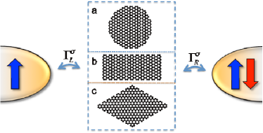
The considered system is displayed in Fig. 1. It consists of a graphene flake that is weakly coupled to external ferromagnetic leads. The coupling strengths are described by and for the left and right leads. We consider graphene flakes of three different hypothetical shapes: circular, rectangular and rhombic. It is assumed that the system can be in two magnetic configurations: either parallel or antiparallel one, see Fig. 1.
In order to find the energy levels as well as magnetic moments of graphene quantum dots (GQDs) we have performed exact diagonalization of the following mean-field Hamiltonian
| (1) |
Here, are the hopping integrals, stand for -electron orbitals at site with spin , describes the Stoner splitting, and are the respective occupation numbers. The latter have been computed self-consistently by summing up the squared eigenvectors corresponding to the eigenvalues not greater than the Fermi energy. The hopping integrals are assumed to be nonzero only for nearest neighbors, and the nearest neighbor hopping parameter is set to be equal eV. In turn, the Coulomb on-site repulsion is assumed to be (see e.g. Ref. [Yazyev10, ]). All the GQDs we consider are of comparable area (9 nm2) and consist of 350-400 carbon atoms. Here we focus on the shapes with a relatively small number of zigzag type edge atoms, and consequently few quasi-degenerate edge states in the vicinity of the Dirac point for U=0 (for triangular and hexagonal structures with purely zigzag edges see Refs. [Fernandez07, ; Potasz12, ]).
Exact diagonalization of the Hamiltonian (1) yields the eigenvalues that have been then used as an input to the mean-field Hamiltonian for the graphene quantum dot
| (2) |
Here, is the phenomenological charging energy of the dot, is the energy of the dot’s orbital discrete level for spin , denotes the particle number operator for the level , , and is the number of electrons in an electrically neutral quantum dot.
The leads are modeled by Hamiltonian of noninteracting quasi-particles
| (3) |
where creates a spin- electron with wave vector in lead and is the corresponding energy. In turn, tunneling processes between the dot and the leads are described by
| (4) |
with denoting the hopping matrix element between the dot level and the lead . The broadening of the GQD’s levels can be described by , where is the spin-dependent density of states in the lead for spin subband . In the case of ferromagnetic leads this can be then written as, , with and being the spin polarization of lead . Here, () corresponds to the coupling to the majority (minority) spin band. In the following we assume, and . Furthermore, in numerical calculations, for all three different shapes of the dots, we have also assumed the charging energy eV and the coupling strength eV. The value has been found from a scaling law (against QD-size) formulated in Ref. [Ma09, ]. Incidentally, this scaling leads also to acceptable estimations of charging energies in Ref. [ponomarenko08, ; stampfer08, ].
In order to reliably determine the transport properties of Coulomb-blockade graphene quantum dots weakly coupled to external leads, we employ the real-time diagrammatic technique. diagrams ; thielmann ; weymannPRB08 This technique relies on systematic perturbation expansion of the reduced density matrix and the operators of interest in the dot-lead coupling strength . The calculation proceeds with the determination of respective self-energy matrices , which enables the evaluation of the elements of the reduced density matrix of GQD by using the following master-like equation thielmann
| (5) |
Here, is the vector containing stationary probabilities, is the modified self-energy matrix so as to include the normalization of probabilities and labels the states of the graphene quantum dot. Having found the occupation probabilities, the current flowing through the system can be calculated using the following equation thielmann
| (6) |
where is the modified self-energy matrix to account for the number of electrons transferred through the system.
By performing the perturbation expansion of the respective self-energies one is then able to calculate the current order by order in tunneling processes. In this paper we have included the first and second-order self-energies. The first order of expansion corresponds to sequential tunneling, which dominates transport outside the Coulomb blockade regime, whereas the second-order self-energies describe the cotunneling processes. Cotunneling processes occur through virtual states of the system and are dominant in the Coulomb blockade regime. cotunneling Thus, to properly describe the transport properties of the system in the full range of bias and gate voltages, it is of vital importance to include both the first and second order terms of the perturbation expansion.
With the aid of the real-time diagrammatic technique, we have determined the behavior of the current , differential conductance and tunnel magnetoresistance TMR of graphene quantum dots in both the linear and nonlinear response regimes. In addition, we have also calculated the bias and gate voltage dependence of the shot noise and the corresponding Fano factor . thielmann The Fano factor is defined as, , and describes deviation of the shot noise from the Poissonian value, relevant for uncorrelated tunneling events. blanterPR00 The main results and their discussion are presented in the sequel.
III Results and discussion
Below we present numerical results on transport through graphene quantum dots of similar sizes (in terms of the number of atoms), but different shapes. For simplicity, we assume the Fermi level of the leads to be equal to the Fermi level of a neutral graphene. We show that the corresponding energy spectra are strongly dependent on the GQD geometry, and that the emerging magnetic moments are essentially localized at zigzag-like segments of the dots’ edges. This leads to different transport characteristics of particular GQDs, as shown and discussed in the following. More specifically, we show that the size of blockade regions (blockade diamonds in the bias-gate voltage dependence of the differential conductance) can be used to gain some information about the edge states. As it is well known, the size of the diamonds is determined by the Coulomb charging energy and the level spacing. Therefore, the sequence of diamonds depends on whether a given level is spin degenerate or not. The absence of spin degeneracy, in turn, implies the presence of magnetic states. Since the edge states are either in the center of the energy gap or close to it, the corresponding diamonds can be easily identified.
III.1 Rhombic graphene dots
Let us begin our considerations with the case of graphene flake of rhombic geometry with exclusively armchair-type edges. The atomic structure of the graphene dot and the corresponding energy spectrum measured from the Fermi level, , is shown in Fig. 2. As one can see in this figure, the rhombic graphene flake has neither low-energy localized states nor magnetic moments at the edges. Moreover, the energy levels of the dot are independent of the Coulomb parameter , which is a consequence of the absence of magnetized states. As one can readily see, such a structure has therefore a quite pronounced energy gap at the Fermi level. Thus, the armchair-edge rhombic geometry may be suitable for engineering graphene nanostructures useful for field effect transistor devices (with a pronounced ON/OFF current ratio).
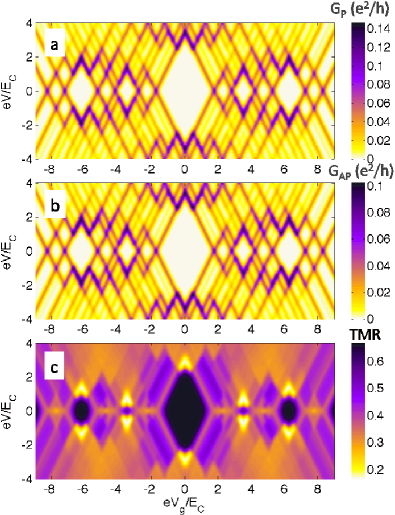
The bias and gate voltage dependence of the differential conductance in the parallel and antiparallel configurations is shown in Figs. 3(a) and 3(b). The central white region corresponds to zero excess electrons in the dot. This region is relatively large due to the large energy gap. With sweeping the gate voltage, one shifts the position of the graphene dot levels, changing thus the number of electrons in the dot. Due to particle-hole symmetry the spectrum is symmetric with respect to the central diamond. The second diamond (with increasing gate voltage starting from ) is much smaller, when compared to the middle one, as it is determined only by the charging energy . The next diamond, apart from the charging energy, also includes the level spacing between the first and second levels (for positive or negative energies). Since each level is spin degenerate, every second diamond (to the left or to the right of the central diamond) is determined only by the charging energy and therefore all of them are relatively small. The other diamonds include additionally the level spacing and are therefore larger. Thus, the level spacings and the energy gap can, in principle, be determined from the size of the corresponding blockade diamonds.
Except for particular structure of the Coulomb diamonds related with the energy spectrum of the dot, which is independent of the magnetic configuration of the device, one can see that the differential conductance in the parallel configuration is larger than that in the antiparallel configuration . This is related with the asymmetry in the couplings to the spin majority and spin minority bands of the ferromagnets. For the parallel configuration, the majority-majority channel is most conducting, while in the antiparallel configuration there are two weakly conducting majority-minority channels. As a consequence, . The difference between the system transport properties in these two magnetic configurations is described by the tunnel magnetoresistance, defined as, julliere , with and denoting the resistance in the parallel and antiparallel magnetic configurations of the device. The bias and gate voltage dependence of TMR is shown in Fig. 3(c). First of all, one can see that the TMR is always positive, as in typical spin-value quantum dot devices. weymannPRB05 The TMR is particularly enhanced in the central Coulomb blockade diamond [black area in Fig. 3(c)], where the sequential tunneling is exponentially suppressed while transport takes place via cotunneling events. In this transport regime the dot is empty and the current is driven by elastic cotunneling processes. weymannPRB05 ; weymannPRB08 The TMR is then exactly given by the Julliere value, julliere , which for the assumed parameters yields . In other Coulomb diamonds, the inelastic cotunneling processes become relevant and the TMR is generally smaller than Julliere’s value. Similar behavior can be observed in the sequential tunneling regime, where the TMR is much smaller than . This is related with the fact that the information about magnetic configuration of the device is now transferred by uncorrelated sequential tunneling events and the non-equilibrium spin accumulation which builds up in the graphene quantum dot. This mechanism is less effective than direct spin-conserving cotunneling between the left and right lead, thus the TMR is smaller than Julliere’s value.
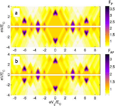
The Fano factors in the parallel and antiparallel magnetic configurations of the device are shown in Fig. 4. In both cases, the shot noise in the blockade regions, where cotunneling processes dominate, is generally super-Poissonian, i.e. the corresponding Fano factors are larger than unity, . This is related with bunching of inelastic cotunneling events sukhorukovPRB01 and has already been observed experimentally in transport through other quantum dot systems. onac06 ; zhang Interestingly, in the central diamond, where elastic cotunneling mediates the current, the Fano factors in both magnetic configurations approach unity. This is due to the fact that the elastic cotunneling processes are uncorrelated in time and the shot noise is Poissonian. In the regions, where transport is dominated by sequential tunneling processes, the corresponding shot noise is rather sub-Poissonian with the relevant Fano factors smaller than 1, . This suppression of the noise is due to Coulomb correlations between consecutive sequential tunneling processes. We note, that the calculations include also the thermal noise, which is dominant in the small bias voltage regime. Accordingly, when tends to zero, the current and shot noise both tend to zero, and the noise is dominated by the thermal noise (nonzero also at ). Thus, the corresponding Fano factor diverges when , as marked with a horizontal stripe in Fig. 4.
III.2 Circular graphene dots
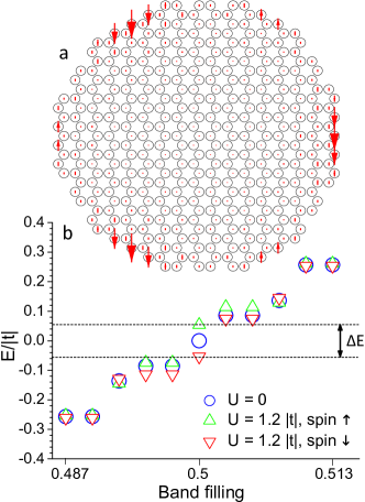
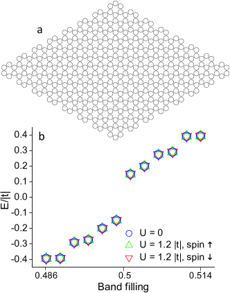
Let us now have a closer look at the circular graphene flake. In this geometry the edge atoms have rather short zigzag-like (and armchair-like) coordinations. Consequently, any complete compensation of the edge magnetization (antiferromagnetic alignment) can be hardly realized on geometrical grounds. Our calculations show that indeed the ground state magnetic configuration of the edges is ferromagnetic-like (ferrimagnetic), but with some admixture of antiparallel magnetic moments. In this situation there is no way to control spin dependent electric current with external magnetic field, unless one makes use of ferromagnetic electrodes.
When (nonmagnetic dot), there is no gap at the Fermi level. However, as shown in Fig. 5, the presence of edge magnetism () leads to the opening of an energy gap at the Fermi level. Noteworthy, near the half-band filling the highest occupied energy levels are fully spin-polarized - the dot behaves as a magnetic one. The overall magnetic moment of the dot shown in Fig. 5 is equal to . This, in turn, affects the spin-resolved transport properties of the system, which now show some asymmetry with respect to the bias and gate voltage reversal.
Incidentally, in accordance with Lieb’s theorem, lieb89 one can increase the net magnetic moment up to , by modifying the edges so as to increase the imbalance of the numbers and of the A(B)-sublattice atoms. Our results are rather robust against moderate edge disorder. In particular, when a few edge atoms are removed then possible implications are consistent with predictions based on the aforementioned theorem. Noteworthy, the asymmetry seen in Fig. 6 provides direct visualization of the presence of GQD’s uncompensated spin. In another context as the present one, the edge state effects on the electronic structure as well as charge and spin transport have been studied in Refs. [Libisch09, ; Wimmer08, ].
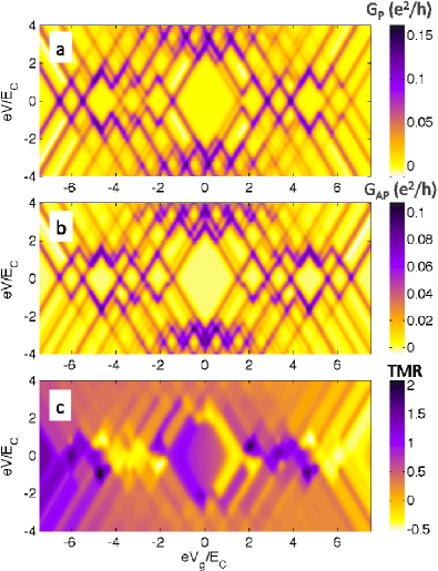
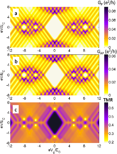
The differential conductance spectra in both magnetic configurations are shown in Fig. 6. First, we note that in equilibrium all the states of negative energy are occupied and the dot has one unpaired spin-down electron. The addition of a new electron costs then the charging energy plus half the level spacing , see Fig. 5. Note that the added electron is a spin-up one. This corresponds to the large central diamond in Fig. 6. The subsequent electron occupies spin-down level and the corresponding addition energy includes the Coulomb charging energy plus the spacing between the first and second levels of positive energy. Since the latter spacing is mach smaller than , the corresponding diamond is smaller than the central one, but it is still larger than the diamond determined by only. It indicates that this state is magnetic. The next electron occupies again the spin-down level, which is almost degenerate with the previous level. The corresponding diamond is determined practically by the charging energy and is therefore smaller than the preceding one. The following two electrons occupy the two spin-up states (also almost degenerate), so the corresponding two diamonds are determined by the charging energy plus the level spacing and charging energy, respectively. Similar scenario holds for higher gate voltages, when higher energy levels become occupied by electrons, as well as to negative gate voltages.
It is also worth noting that now the spectra are significantly different from the corresponding ones for , see Fig. 5. Since for there is no gap at the Fermi level, the central diamond should be then determined by the charging energy only and therefore should be small. The second diamond should be relatively large while the three subsequent diamonds should be small and determined by the charging energy. Thus, the conductance spectra can be used to distinguish the situation with nonzero from that with .
Apart from the typical Coulomb blockade diamonds described above, the transport characteristics display an asymmetry with respect to the bias reversal, see Fig. 6. This is due to the spin splitting of the GQD’s levels. In addition, in certain transport regimes one can find a negative differential conductance, which is present in both magnetic configurations. This effect is basically related with the fact that for certain transport voltages electrons participating in transport are mainly spin-down (minority-spin) ones and the current is thus decreased.
The difference between the currents flowing through the system in the two magnetic configurations of the device results in the TMR effect shown in Fig. 6c. Because now the energy eigenstates of the graphene dot are no longer spin degenerate, one can observe a nontrivial behavior of the TMR as a function of both the bias and gate voltages. First of all, it can be seen that in certain transport regimes the TMR can take values much larger than those given by Julliere’s model. Furthermore, there are transport regimes where TMR changes sign and becomes negative. To explain this behavior we will refer to approximate formulas for sequential tunneling and cotunneling currents. Suppose the temperature is much larger than the coupling strength , but still smaller than the charging energy , . Then, transport is mainly determined by thermally-activated sequential tunneling. The current is thus proportional to, . If transport occurs through the spin-up level of the dot, the current in the parallel configuration is, , while for the antiparallel configuration one finds, , which yields for the TMR, . If, in turn, the current is related with tunneling through spin-down levels, one gets and for the parallel and antiparallel configurations, respectively, and the TMR is now negative, . On the other hand, if the temperature is comparable to the coupling strength, , the current is mainly due to cotunneling processes. Its dependence on the spin polarization of the leads can be found if one considers elastic cotunneling regime, where . Then, if cotunneling occurs through spin-up levels, the currents in the two configurations are proportional to, , , yielding , which for the assumed parameters () gives, . Note that now , i.e. one obtains maximum TMR three times larger than in the case of rhombic-like graphene flake discussed in the previous section. However, if cotunneling occurs through spin-down levels, the current in the antiparallel configuration is the same as above, while the current in the parallel configuration becomes, , which results in . For the assumed parameters one then finds, , i.e. the system exhibits a large-magnitude negative TMR. Because the calculations are performed for , one finds that the TMR in the Coulomb diamonds is much enhanced compared to Julliere’s value, with , if transport is due to spin-up states of the graphene dot. On the other hand, if spin-down states are active in transport a negative TMR occurs with, . These values of the TMR can be clearly seen in Fig. 6c.
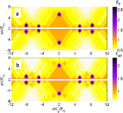
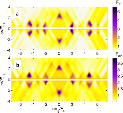
The corresponding Fano factors in both magnetic configurations are shown in Fig. 7. In both cases, the shot noise is generally super-Poissonian in the Coulomb blockade regions, where cotunneling processes dominate, and bunching of inelastic events enhances the noise. In other regimes transport is dominated by sequential tunneling processes and the corresponding shot noise is sub-Poissonian, . As before, this is due to the Coulomb correlations between sequential tunneling events and the Pauli exclusion principle, resulting in suppressing of the noise.
III.3 Rectangular graphene dots
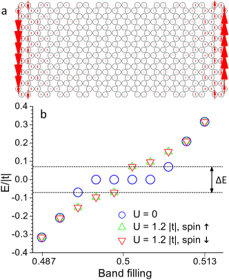
In this subsection, transport through a rectangular graphene quantum dot with zigzag and armchair edges is studied. In contrast to the cases discussed earlier, with either nonmagnetic edges (rhombus dot) or nearly ferromagnetically aligned ones (circular dot), the present case corresponds to a spontaneous antiparallel alignment of magnetic edges. This device may therefore act as an effective spin-valve or a magnetoresistive sensor, and appears potentially useful for spintronics. Son06 ; Maassen11
Figure 8 presents atomic structure of the considered graphene flake and the corresponding energy spectrum. It can bee seen that for a sufficiently large on-site Coulomb repulsion parameter , an energy gap opens in the energy spectrum, resulting in a metal/semiconductor (zero-gap/finite-gap semiconductor) transition. Moreover, the energy levels of this graphene dot remain spin degenerate (perfect compensation of the net magnetization), in contrast to the case of the circular dot.
The subsequent figures show the corresponding bias and gate voltage dependence of the differential conductance and TMR, see Fig. 9, as well as the Fano factor, see Fig. 10. Since there is a gap at the Fermi level, the central diamond in the differential conductance is now rather large and includes the charging energy plus a half of the energy gap. Because the energy levels are now spin degenerate, every second diamond is smaller, as it is determined merely by the charging energy . Moreover, because of the spin degeneracy of the levels, the differential conductance in the parallel configuration is always larger than that in the antiparallel configuration, yielding positive TMR, see Fig. 9. The behavior of TMR resembles that in the case of the rhombic graphene flake. The TMR is given by Julliere’s value in the Coulomb diamonds where elastic cotunneling drives the current, and is much more suppressed in the other diamonds with either inelastic cotunneling or sequential tunneling.
The bias and gate voltage dependence of the Fano factor in both magnetic configurations of the device is shown in Fig. 10. The general features of these spectra are qualitatively similar to those discussed earlier in the case of the rhombic-like graphene dots: in the Coulomb blockade regions when elastic cotunneling is relevant, in the blockade regions when inelastic cotunneling is present, and in the sequential tunneling regime.
IV Conclusions
In this paper we have analyzed transport properties of graphene quantum dots of different geometries in the presence of the on-site Coulomb repulsion. Characteristic features due to GQD edges are shown to be reflected in the Coulomb blockade diamonds and other transport characteristics. It has been demonstrated that the TMR effect in graphene quantum dots may be quite large, much larger then the corresponding Julliere’s value of TMR. In turn, the shot noise was found to take both sub-Poissonian as well as super-Poissonian values. Out of the three graphene flake shapes studied here, the armchair-edge rhombus flake shows no magnetism, the circular flake has uncompensated ferrimagnetic edge configuration, whereas the rectangular flake displays antiparallelly aligned zigzag-edge magnetizations. All these features manifest themselves in transport characteristics, providing information about the geometry and edge states of graphene dots.
In frame of the model assumed, the conductance spectra can be used to check whether the energy spectrum includes zero energy levels or not. If they do, then the first diamonds are determined only by the charging energy and are small. If not, then the central diamonds are large as they include not only the charging energy, but also the level separation due to the size quantization. However, the model is not free from some limitations, so the conductance spectra in real situations may be different. Accordingly, the conclusions concerning magnetic edge states should rather be regarded as indicative only. First of all, the description is based on mean-field approximation for charging energy and also for the coupling parameter . In reality, both parameters may depend on the particular states taking part in transport. As already mentioned in the introduction, this may be especially important for , when transport occurs via localized edge states. As the variation of has some influence on the size of the Coulomb diamonds, the variation of modifies mainly the conductance and TMR, leaving the size of the diamonds unchanged. Being aware of all the underlying assumptions, we believe our results present a sound starting point aimed at transport characterization of the electronic states (including also the edge states) of graphene flakes. Since both the crucial parameters (especially the coupling parameter ) depend on a particular experimental realization, a more accurate description can be performed when the relevant experimental data are available.
This work was supported by the Polish Ministry of Science and Higher Education as a research project No. N N202 199239 for years 2010-2013. I.W. also acknowledges support from the Alexander von Humboldt Foundation and the 7FP of the EU under REA grant agreement No CIG-303 689.
References
- (1) K.S. Novoselov, A.K. Geim, S.V. Morozov, D. Jiang, Y. Zhang, S.V. Dubonos, I.V. Grigorieva, A.A. Firsov, Science 306, 666 (2004).
- (2) A. K. Geim and K. S. Novoselov, Nature Mater. 6, 183 (2007).
- (3) M. I. Katsnelson, Mater. Today 10, 20 (2007).
- (4) A. H. Castro Neto, F. Guinea, N. M. R. Peres, K. S. Novoselov and A. K. Geim, Rev. Mod. Phys. 81, 109 (2009).
- (5) N. Tombros, C. Jozsa, M. Popinciuc, H. T. Jonkman and B. J. van Wees, Nature 448, 571 (2007).
- (6) F. Sols, F. Guinea, and A. H. Castro Neto, Phys. Rev. Lett. 99, 166803 (2007).
- (7) L. A. Ponomarenko, F. Schedin, M. I. Katsnelson, R. Yang, E. W. Hill, K. S. Novoselov, A. K. Geim, Science 320, 356 (2008).
- (8) C. Stampfer, J. Guttinger, F. Molitor, D. Graf, T. Ihn, and K. Ensslin, Appl. Phys. Lett. 92, 012102 (2008).
- (9) K. Todd, H.-T. Chou, S. Amasha, and D. Goldhaber-Gordon, Nano Letters 9, 416 (2009).
- (10) M. Fujita, K. Wakabayashi, K. Nakada, and K. Kusakabe, J. Phys. Soc. Jpn. 65, 1920 (1996).
- (11) O. V. Yazyev, Rep. Prog. Phys. 73, 056501 (2010).
- (12) M. Acik and Y. J. Chabal, Jap. J. Appl. Phys. 50, 070101 (2011).
- (13) Z. Klusek, Z. Waqar, E. Denisov, T. Kompaniets, I. Makarenko, A. Titkov, and A. Bhatti, Appl. Surf. Sci. 161, 508 (2000).
- (14) Y. Kobayashi, K.-i. Fukui, T. Enoki, K. Kusakabe, and Y. Kaburagi, Phys. Rev. B 71, 193406 (2005).
- (15) P. Sutter, Nature Mater. 8, 171 (2009).
- (16) Y.-W. Son, M. L. Cohen, and S. G. Louie, Nature (London) 444, 347 (2006).
- (17) W.Y. Kim and K. S. Kim, Nature Nanotech. 3, 408 (2008).
- (18) F. Muñoz-Rojas, J. Fernández-Rossier, and J. J. Palacios, Phys. Rev. Lett. 102, 136810 (2009).
- (19) W. Han, K.M.McCreary, K. Pi, W.H.Wang, Y. Li, H. Wen, J.R. Chen, R.K. Kawakami, J. Mag. Mag. Mat. 324, 369 (2011).
- (20) S. Krompiewski, Phys. Rev. B 80, 075433 (2009).
- (21) I. Weymann, J. Barnaś, and S. Krompiewski, Phys. Rev. B 76, 155408 (2007); 78, 035422 (2008).
- (22) B. Zhou, X. Chen, H. Wang, K. -H. Ding, G. Zhou, J. Phys.: Condens. Matter 22, 445302 (2010).
- (23) C. Tao, L. Jiao, O. V. Yazyev, Y.-C. Chen, J. Feng, X. Zhang, R. B. Capaz, J. M. Tour, A. Zettl, S. G. Louie, H. Dai, and M. F. Crommie, Nat. Phys. 7, 616 (2011).
- (24) D. A. Areshkin and B. K. Nikolić, Phys. Rev. B 79, 205430 (2009).
- (25) M. Zwierzycki and S. Krompiewski, Acta Physica Polonica A 118, 856 (2010).
- (26) S. Krompiewski, Nanotechnology, 22, 445201 (2011); ibidem, 23, 135203 (2012).
- (27) J. Fernández-Rossier and J. J. Palacios, Phys. Rev. Lett. 99, 177204 (2007).
- (28) P. Potasz, A. D. Güçü, A. Wójs, and P. Hawrylak, Phys. Rev. B 85, 075431 (2012).
- (29) Q. Ma, T. Tu, Z.-R. Lin, G.-C. Guo, G.-P. Guo, cond-mat/0911.2845v1 (2009).
- (30) H. Schoeller and G. Schön, Phys. Rev. B 50, 18436 (1994); J. König, J. Schmid, H. Schoeller, and G. Schön, Phys. Rev. B 54, 16820 (1996).
- (31) A. Thielmann, M. H. Hettler, J. König, and G. Schön, Phys. Rev. Lett. 95, 146806 (2005); Phys. Rev. B 68, 115105 (2003).
- (32) I. Weymann, Phys. Rev. B 78, 045310 (2008).
- (33) D. V. Averin and Yu. V. Nazarov, Phys. Rev. Lett. 65, 2446 (1990); K. Kang and B. I. Min, Phys. Rev. B 55, 15412 (1997).
- (34) J. Maassen, W. Ji, and H. Guo, Nano Lett. 11, 151 (2011).
- (35) Ya. M. Blanter and M. Büttiker, Phys. Rep. 336, 1 (2000).
- (36) I. Weymann, J. König, J. Martinek, J. Barnaś, and G. Schön, Phys. Rev. B 72, 115334 (2005).
- (37) M. Julliere, Phys. Lett. A 54, 225 (1975).
- (38) E. V. Sukhorukov, G. Burkard, and D. Loss, Phys. Rev. B 63, 125315 (2001).
- (39) E. Onac, F. Balestro, B. Trauzettel, C. F. J. Lodewijk, and L. P. Kouwenhoven, Phys. Rev. Lett. 96, 026803 (2006).
- (40) Y. Zhang, L. DiCarlo, D. T. McClure, M. Yamamoto, S. Tarucha, C. M. Marcus, M. P. Hanson, and A. C. Gossard, Phys. Rev. Lett. 97, 036603 (2007).
- (41) E. H. Lieb, Phys. Rev. Lett. 62, 1201 (1989).
- (42) F. Libisch, C. Stampfer, and J. Burgdörfer, Phy. Rev. B 79, 115423 (2009).
- (43) M. Wimmer, I. Adagideli, S. Berber, D. Tománek, and K. Richter, Phys Rev. Lett. 100, 177207 (2008).