Origin of the different conductive behavior in pentavalent-ion-doped anatase and rutile TiO2
Abstract
The electronic properties of pentavalent-ion (Nb5+, Ta5+, and I5+) doped anatase and rutile TiO2 are studied using spin-polarized GGA+U calculations. Our calculated results indicate that these two phases of TiO2 exhibit different conductive behavior upon doping. For doped anatase TiO2, some up-spin-polarized Ti 3d states lie near the conduction band bottom and cross the Fermi level, showing an n-type half-metallic character. For doped rutile TiO2, the Fermi level is pinned between two up-spin-polarized Ti 3d gap states, showing an insulating character. These results can account well for the experimental different electronic transport properties in Nb (Ta)-doped anatase and rutile TiO2.
Transparent conducting oxides (TCOs) have many applications in optoelectronic devices such as flat panel displays, organic light-emitting diodes and solar cells. As one of the TCOs, Sn-doped In2O3 is widely used because of its excellent optical transparency and electrical transport property.Edwards et al. (2004) However, owning to the high cost of indium and the increasing demand for high-performance TOCs, many efforts have been made to develop new TOCs materials.Tadatsugu (2005); Wang et al. (2010) Recently, as one potential candidate of TCOs, Nb (Ta)-doped anatase TiO2 has attracted lots of attention because of its high electrical conductivity and optical transparency.Furubayashi et al. (2005); Hitosugi et al. (2005); Furubayashi et al. (2006a, 2007); Gillispie et al. (2007a, b); Hoang et al. (2008); Archana et al. (2011) However, the origin of its high conductivity is still controversial. Wan et al.Wan and Wang (2006) found that Nb-doped TiO2 grown on (0001) Al2O3 substrate shows a much larger resistivity than that grown on (100) SrTiO3 substrate, and hence the Nb diffusion into the SrTiO3 substrate is thought to lead to the high conductivity of Nb-doped TiO2. Meanwhile, Furubayashi et al.Furubayashi et al. (2006b) confirmed that Nb-doped TiO2 forms a rutile phase on the (0001) Al2O3 substrate but an anatase phase on the other substrates, and hence they suggested that the higher resistivity of Nb-doped TiO2 grown on (0001) Al2O3 substrates is caused by the formation of rutile phase. Interestingly, later experiments further verified that Nb (Ta)-doped anatase TiO2 is metallic but Nb (Ta)-doped rutile TiO2 is insulating.Zhang et al. (2007); Barman et al. (2011) Therefore, one may speculate that the Nb (Ta) doping can lead to different conductive properties in anatase and rutile TiO2, i.e., conductive for anatase phase but insulating for rutile phase.Yang et al. (2009a)
In principle, a pentavalent dopant, such as Nb5+, Ta5+, and I5+,Yang et al. (2008, 2012) can release one additional electron into TiO2 than a Ti4+, and introduce donor levels.Finazzi et al. (2008); Hitosugi et al. (2008) Although Nb-doped anatase TiO2 has been studied using standard density functional theory (DFT) calculations,Hitosugi et al. (2008); Liu et al. (2008); Kamisaka et al. (2009) the standard DFT calculations within either local density approximation (LDA) or generalized gradient approximation (GGA) cannot properly deal with the strong-corrected Ti 3d electrons.Finazzi et al. (2008); Yang et al. (2010) In the present work, we studied the electronic properties of pentavalent-ion (Nb5+, Ta5+, and I5+) doped anatase and rutile TiO2, respectively, using spin-polarized GGA+U calculations which can give a proper description of Ti 3d orbitals.Finazzi et al. (2008); Yang et al. (2010, 2009b). Our calculations indicate that Nb (Ta, I)-doped anatase TiO2 shows an n-type half-metallic character, while Nb (Ta, I)-doped rutile TiO2 shows an insulating character. These results give a good explanation for experimentally observed different conductive behavior in Nb (Ta)-doped TiO2.
The spin-polarized GGA+U electronic structure calculations were carried out using the Vienna ab-inito simulation package (VASP).Kresse and Furthmüller (1996); Kresse and Furthm ller (1996) 108-atom supercell of the anatase phase and 72-atom supercell of the rutile phase are used to model Nb (Ta, I)-doped TiO2, in which a Ti atom is substituted by a Nb (Ta, I) atom. The projector augmented wave (PAW) potentials are used to treat electron-ion interactions and generalized gradient approximation parameterized by Perdew and Wang (PW91) are used for electron exchange-correction functional.Blöchl (1994); Perdew and Wang (1992) A cut-off energy of 500 eV and a k-point mesh centered at point are used. The lattice parameters and all the atomic positions are fully relaxed until all components of the residual forces are smaller than 0.01 eV/Å. In our GGA+U calculations, the on-site effective U parameter (Ueff=U-J=5.8 eV) proposed by Dudarev et al. is adopted for Ti 3d electrons.Dudarev et al. (1998); Anisimov et al. (1991)
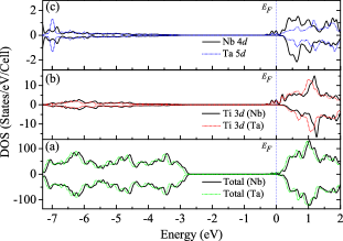
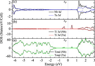
To examine the substitutional Nb (Ta, I) doping effects on the electronic property of TiO2, we calculated the total density of states (TDOS) and partial density of states (PDOS) for Nb (Ta)-doped anatase (see Fig 1) and rutile (see Fig 2), and the TDOS and PDOS for I-doped anatase (see Fig 3) and rutile (see Fig 4). For Nb (Ta)-doped anatase TiO2, the calculated TDOS shows that it is spin-polarized, and some up-spin-polarized gap states extend from the conduction band (CB) into the band gap. These up-spin-polarized gap states are located just below the CB bottom, and cross the Fermi level, indicating an n-type half-metallic character. This is in good agreement with the experimentally observed excellent conductive property in Nb (Ta)-doped anatase TiO2.Furubayashi et al. (2005); Hitosugi et al. (2005); Furubayashi et al. (2006a, 2007); Gillispie et al. (2007a, b); Hoang et al. (2008); Archana et al. (2011) The PDOS shows the Nb 4d (Ta 5d ) states mix with the Ti 3d states in the whole CB, indicating that the Nb (Ta) dopant forms a strong Nb (Ta)-O bond. It is also noted that the up-spin Ti 3d orbitals strongly hybridize with the Nb 4d (Ta 5d ) orbitals, and as will be further discussed below, the Ti 3d orbitals mostly contribute to the up-spin gap states. For Nb (Ta)-doped rutile phase (see Fig. 2), as in the case of doped anatase, Nb 4d (Ta 5d ) states spread over the whole CB, and two fully spin-polarized gap states with a gap about 1.1 eV lie in the band gap. Its PDOS shows that these two gap states are also mainly contributed by the Ti 3d states, however, the Fermi level lies between the two gap states, showing an insulating character. These calculated results can account for the experimentally observed much higher resistivity in Nb (Ta)-doped rutile phase than the anatase phase.Wan and Wang (2006); Furubayashi et al. (2006b); Zhang et al. (2007); Barman et al. (2011)
In addition, it is worth mentioning that our calculated results are different from previous GGA+U calculations done by Morgan et al.,Morgan et al. (2009) in which the Nb (Ta)-doped anatase and rutile TiO2 both show insulating properties. This discrepancy may be attributed to the following two reasons: (1) Morgan et al. applied a U parameter of 4.2 eV for Ti 3d electrons, which is much smaller than the used value of 5.8 eV in this work. (2) In our GGA+U calculations, all the degrees of the freedom for Nb (Ta)-doped TiO2, including lattice parameters and all the atomic positions, are fully relaxed. In contrast, in Morgan et al.’s calculations, only the internal degrees of freedom are allowed to relax. Therefore, the difference in U values and structural optimization methods may be responsible for the different electronic properties of Nb (Ta)-doped TiO2 in our calculations from those of Margan et al. In fact, Orita also found a metallic character in Nb-doped anatase TiO2 using GGA+U calculations,Orita (2010) in which all the atomic coordinates and lattice constants are optimized. In particular, recent hybrid density functional calculations also show that Nb (Ta)-doped anatase TiO2 is metallic, while Nb (Ta)-doped rutile TiO2 is semiconducting.Yamamoto and Ohno (2012) In summary, these related studies further confirm our GGA+U calculations. As a consequence, we can conclude that the conducting character of Nb (Ta)-doped anatase and the insulating character of Nb (Ta)-doped rutile are their intrinsic properties.
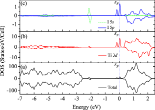
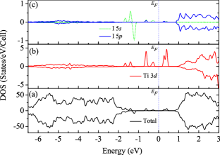
For I-doped anatase and rutile TiO2, similar to the case of Nb (Ta) doping, an n-type half-metallic character occurs in I-doped anatase phase but an insulating character occurs in I-doped rutile phase. The calculated TDOS and PDOS are shown in Fig 3 for anatase phase and Fig 4 for rutile phase. However, different from that of Nb (Ta) doping, a double filled gap state mostly consisting of I 5s orbital appears in the band gap, which is located just above the valence band maximum. This indicates that I dopant exists as I5+ (5s25p0) in TiO2, which is consistent with the standard GGA calculations.Yang et al. (2008)
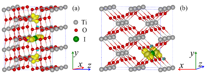
To understand the origin of the different conductive behavior associated with the spin-polarized Ti 3d states in Nb (Ta, I)-doped anatase and rutile TiO2, we take I-doped TiO2 as an example to show its three-dimensional spin density distribution in Fig. 5. For I-doped anatase TiO2, its spin density mostly comes from the four equivalent second-nearest Ti ions around the I dopant (see in Fig. 5a). These four equivalent Ti ions share one electron donated by one I5+ ion with their Ti 3d orbitals, and thus produce a total spin magnetic moment of 1.0 . Therefore, to a first approximation, these four equivalent Ti ions should exist as Ti+3.75 (d1/4). Actually, experimental core-level photoemission spectra measurements showed a minor peak of the binding energy below that of Ti4+ ion,Hitosugi et al. (2008) and this chemical shift corresponds to an increase of the valence electron density on Ti 3d orbitals. For I-doped rutile TiO2, in contrast, its spin density is mainly contributed by the two equivalent second-nearest Ti ions (see Fig 5b). These two Ti ions share one electron and produce a total spin magnetic moment of 1.0 , and thus one can assume that the two equivalent Ti ions exist as Ti+3.5 (d1/2). As a result, it is expected that a lower binding energy of Ti+3.5 ions than that of Ti+3.75 ions can be observed in Nb (Ta, I)-doped rutile TiO2 through experimental core-level photoemission spectra measurements. Furthermore, the increasing of the electron density on Ti 3d orbitals directly leads to the splitting between Ti 3d occupied states and unoccupied states, which is responsible for the insulating character of I-doped rutile TiO2. Similar spin density distributions also occur in Nb (Ta)-doped anatase and rutile TiO2.
In summary, we studied the electronic properties of Nb (Ta, I)-doped anatase and rutile TiO2 by spin-polarized GGA+U calculations. In doped anatase TiO2, the Fermi level is pinned in some up-spin-polarized gap states near the CBM, showing an n-type half-metallic conductive property. In doped rutile, in contrast, two localized states with a gap about 1.1 eV are introduced in the band gap, and the Fermi level lies between them, showing an insulating character. Therefore, to prepare the TiO2-based TCOs through pentavalent-ion-doping, it is essential to avoid the phase transition from anatase to rutile. Our theoretical calculations may provide some useful guidance to develop TiO2-based TCOs.
Acknowledgements.
This work is supported by the National Basic Research Program of China (973 program, 2007CB613302), National Science foundation of China under Grant 11174180 and 20973102, and the Natural Science Foundation of Shandong Province under Grant number ZR2011AM009. Y.P.F is thankful for the support of the Singapore National Research Foundation Competitive Research Program (Grant No. NRF-G-CRP 2007-05).References
- Edwards et al. (2004) P. P. Edwards, A. Porch, M. O. Jones, D. V. Morgan, and R. M. Perks, Dalton T. , 2995 (2004).
- Tadatsugu (2005) M. Tadatsugu, Semicond. Sci. Tech. 20, S35 (2005).
- Wang et al. (2010) L. Wang, D. W. Matson, E. Polikarpov, J. S. Swensen, C. C. Bonham, L. Cosimbescu, J. J. Berry, D. S. Ginley, D. J. Gaspar, and A. B. Padmaperuma, J. Appl. Phys. 107, 043103 (2010).
- Furubayashi et al. (2005) Y. Furubayashi, T. Hitosugi, Y. Y. K. Inaba, G. Kinoda, Y. Hirose, T. Shimada, and T. Hasegawa, Appl. Phys. Lett. 86, 252101 (2005).
- Hitosugi et al. (2005) T. Hitosugi, Y. Furubayashi, A. Ueda, K. Itabashi, K. Inaba, Y. Hirose, G. Kinoda, Y. Yamamoto, T. Shimada, and T. Hasegawa, Jpn. J. Appl. Phys 44, L1063 (2005).
- Furubayashi et al. (2006a) Y. Furubayashi, T. Hitosugi, Y. Yamamoto, Y. Hirose, G. Kinoda, K. Inaba, T. Shimada, and T. Hasegawa, Thin Solid Films 496, 157 (2006a).
- Furubayashi et al. (2007) Y. Furubayashi, N. Yamada, Y. Hirose, Y. Yamamoto, M. Otani, T. Hitosugi, T. Shimada, and T. Hasegawa, J. Appl. Phys. 101, 093705 (2007).
- Gillispie et al. (2007a) M. A. Gillispie, M. F. A. M. v. Hest, M. S. Dabney, J. D. Perkins, and D. S. Ginley, J. Appl. Phys. 101, 033125 (2007a).
- Gillispie et al. (2007b) M. A. Gillispie, M. F. v. Hest, M. S. Dabney, J. D. Perkins, and D. S. Ginley, J. Mater. Res. 22, 2832 (2007b).
- Hoang et al. (2008) N. L. H. Hoang, N. Yamada, T. Hitosugi, J. Kasai, S. Nakao, T. Shimada, and T. Hasegawa, Appl. Phys. Express 1, 115001 (2008).
- Archana et al. (2011) P. S. Archana, R. Jose, M. M. Yusoff, and S. Ramakrishna, Appl. Phys. Lett. 98, 152106 (2011).
- Wan and Wang (2006) Q. Wan and T. H. Wang, Appl. Phys. Lett. 88, 226102 (2006).
- Furubayashi et al. (2006b) Y. Furubayashi, T. Hitosugi, and T. Hasegawa, Appl. Phys. Lett. 88, 226103 (2006b).
- Zhang et al. (2007) S. X. Zhang, D. C. Kundaliya, W. Yu, S. Dhar, S. Y. Young, L. G. Salamanca-Riba, S. B. Ogale, R. D. Vispute, and T. Venkatesan, J. Appl. Phys. 102, 013701 (2007).
- Barman et al. (2011) A. R. Barman, M. Motapothula, A. Annadi, K. Gopinadhan, Y. L. Zhao, Z. Yong, I. Santoso, Ariando, M. Breese, A. Rusydi, S. Dhar, and T. Venkatesan, Appl. Phys. Lett. 98, 072111 (2011).
- Yang et al. (2009a) K. Yang, Y. Dai, B. Huang, and Y. P. Feng, International Conference on Materials for Advanced Technologies (ICMAT) (2009a).
- Yang et al. (2008) K. Yang, Y. Dai, B. Huang, and M.-H. Whangbo, Chem. Mater. 20, 6528 (2008).
- Yang et al. (2012) K. Yang, Y. Dai, and B. Huang, arXiv:1202.5651v1 [cond-mat.mtrl-sci] (2012).
- Finazzi et al. (2008) E. Finazzi, C. Di Valentin, G. Pacchioni, and A. Selloni, J. Chem. Phys. 129, 154113 (2008).
- Hitosugi et al. (2008) T. Hitosugi, H. Kamisaka, K. Yamashita, H. Nogawa, Y. Furubayashi, S. Nakao, N. Yamada, A. Chikamatsu, H. Kumigashira, M. Oshima, Y. Hirose, T. Shimada, and T. Hasegawa, Appl. Phys. Express 1, 111203 (2008).
- Liu et al. (2008) X. D. Liu, E. Y. Jiang, Z. Q. Li, and Q. G. Song, Appl. Phys. Lett. 92, 252104 (2008).
- Kamisaka et al. (2009) H. Kamisaka, T. Hitosugi, T. Suenaga, T. Hasegawa, and K. Yamashita, J. Chem. Phys. 131, 034702 (2009).
- Yang et al. (2010) K. Yang, Y. Dai, B. Huang, and Y. P. Feng, Phys. Rev. B 81, 033202 (2010).
- Yang et al. (2009b) K. Yang, Y. Dai, and B. Huang, ChemPhysChem 10, 2327 (2009b).
- Kresse and Furthmüller (1996) G. Kresse and J. Furthmüller, Phys. Rev. B 54, 11169 (1996).
- Kresse and Furthm ller (1996) G. Kresse and J. Furthm ller, Comp. Mat. Sci. 6, 15 (1996).
- Blöchl (1994) P. E. Blöchl, Phys. Rev. B 50, 17953 (1994).
- Perdew and Wang (1992) J. P. Perdew and Y. Wang, Phys. Rev. B 45, 13244 (1992).
- Dudarev et al. (1998) S. L. Dudarev, G. A. Botton, S. Y. Savrasov, C. J. Humphreys, and A. P. Sutton, Phys. Rev. B 57, 1505 (1998).
- Anisimov et al. (1991) V. I. Anisimov, J. Zaanen, and O. K. Andersen, Phys. Rev. B 44, 943 (1991).
- Morgan et al. (2009) B. J. Morgan, D. O. Scanlon, and G. W. Watson, J. Mater. Chem. 19, 5175 (2009).
- Orita (2010) N. Orita, Jpn. J. Appl. Phys 49, 055801 (2010).
- Yamamoto and Ohno (2012) T. Yamamoto and T. Ohno, Phys. Rev. B 85, 033104 (2012).