Email: ]ariando@nus.edu.sg
Atomically flat interface between a single-terminated LaAlO3 substrate and SrTiO3 thin film is insulating
Abstract
The surface termination of (100)-oriented LaAlO3 (LAO) single crystals was examined and the growth of SrTiO3 (STO) films on LAO substrates was investigated. Eventually, the atomically flat interface between a single-terminated LAO substrate and STO film was achieved, which is expected to be similar to the n-type interface of two-dimensional electron gas (2DEG),i.e.,(LaO)-(TiO2). Particularly, that can serve as a mirror structure for the typical 2DEG heterostructure to further investigate the origin of 2DEG. This newly developed interface was determined to be highly insulating and remained insulating even after 1 h vacuum reduction. Additionally, this study demonstrates an approach to achieve atomically flat film growth based on LAO substrates.
The high mobility 2DEG generated at the atomically flat interface between LAO films and TiO2-terminated STO substrates was reported for the first time by Ohtomo and Hwang. 1 Since then, 2DEG at the LAO/STO interface has attracted great attention from the community of oxide electronics and been one of the most fascinating topics in the contemporary condensed matter physics. Many intriguing physical properties have been unveiled at such interface by different groups , e.g., the electronically coupled complementary interfaces,2 the transition from metallic to insulating phase as the thickness of LAO films decreases to less than 4 unit cells (uc),3 the magnetic Kondo scattering at the interface,4 the low temperature two-dimensional superconductivity5 and the large gate capacitance enhancement due to strong electron correlations.6 Intriguingly, Ariando et al.7 recently found the coexistence of magnetic and superconducting-like state and proposed electronic phase separation for the 2DEG at the LAO/STO interface. Later the coexistence of superconductivity and ferromagnetism in this system was observed by Dikin et al.8 and Lu Li et al..9 The theoretical origin of this coexistence is attributed to the Ti 3d interface electrons.7,10 Moreover, the integration of 2DEG with Si recently demonstrated by Park et al.11 has pushed this functional oxide interface system forward to nanoelectronic device application.
As to the origin of the metallic conductivity at the LAO/STO interface, generally three different mechanisms have been proposed. The most possible mechanism is the polar discontinuity induced interface charge transfer to overcome polarization catastrophe owing to the polar and nonpolar nature of LAO and STO, respectively.12 The other possible mechanisms are intermixing of La and Ti atoms at the interface13,14 and induced oxygen vacancies15,16 on the STO side due to the oxygen growth pressure or the bombardment during the growth process,17 which could behave similarly as in thermally reduced bulk STO (Ref. 18) and thus lead to metallicity. Additionally, recent studies 19 indicate that the epitaxial strain at the interface seems to play an important role in the interface conductivity.
STO is a widely used substrate for atomically flat interface engineering not only because of its excellent chemical and thermal stabilities and the lattice match with other perovskite oxides, but also the atomically controllable surface termination.20 Similar to STO, LAO is also an excellent substrate and extensively utilized for oxide thin film growth. Moreover, it is extremely difficult to generate conductivity in LAO by thermal treatment because the diffusion coefficient of oxygen vacancies in LAO is very low.21 In addition, oxygen vacancies in LAO, if there is any, are energetically favored to be in energy levels of eV below the conduction band,22 which are too low and nearly impossible to serve as a donor level at room temperature. This is well in contrast to STO, in which the defect level of oxygen vacancies could only be several ten meV below the conduction band,23 and hence gives an advantage over STO for high temperature oxide film deposition.
The surface termination of (100)-oriented LAO single crystals has been previously investigated by Yao et al.24 and Wang et al.25 with multiple surface-sensitive techniques,e.g., time-of-flight scattering and recoiling spectrometry, atomic force microscopy (AFM), low-energy electron diffraction, Auger electron spectroscopy, x-ray photoelectron spectroscopy and reflection electron microscopy. They found that the surface termination of a LAO single crystal is strongly temperature-dependent: the surface is exclusively terminated in a Al-O layer from room temperature up to ∘C and a La-O layer above ∘C; Only in the intermediate temperature region 150 ∘C and 250 ∘C, mixed terminations exist. Using AFM 24 they also demonstrated an atomically flat LAO surface with uniform one-unit-cell step flow, which actually provides the possibility to prepare an atomically flat interface on a LAO substrate. More importantly, the realization and investigation of an atomically flat interface between a LAO substrate and STO film can provide a mirror structure for the typical 2DEG heterostructure, which could be useful for investigating the origin of 2DEG.
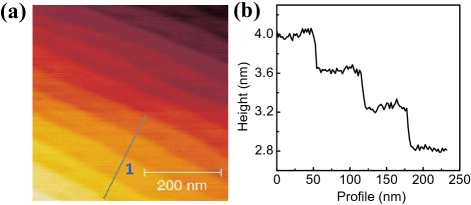
The as-received (100)-oriented LAO single crystals (CrysTec GmbH, Germany) with two sides polished were examined by AFM at room temperature, and indeed the steps on the surfaces were able to be seen, which is consistent with the earlier report.24 Moreover, the surface topography of LAO was largely improved by the subsequent air annealing at 1000 ∘C for 2 hours. The AFM image of an annealed LAO single crystal is shown in Fig. 1(a). As can be seen, the surface is single-terminated and atomically flat with uniform steps. The profile data in Fig. 1(b) corresponding to the cross line mark by ‘1’ in Fig. 1(a) displays the average terrace width of nm and the average step height of Å pertaining to 1 uc of LAO.
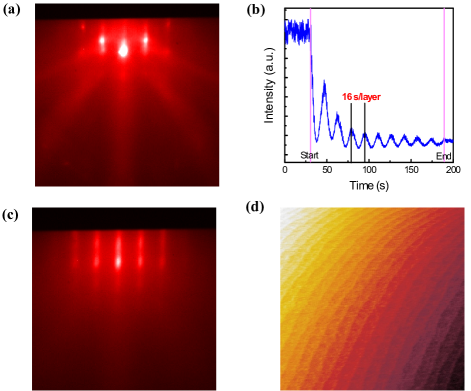
In our work, pulsed laser deposition with a KrF excimer laser ( nm) was used. STO films were deposited from a single crystal STO target on fully-terminated LAO single crystal substrates at 800 ∘C and oxygen pressure of mbar, which are typical conditions for 2DEG growth. Before deposition, LAO substrates were kept under the deposition conditions for 30 mins for the stabilization of surface termination. The reflection high-energy electron diffraction (RHEED) was utilized to monitor the entire growth process. The RHEED pattern of a LAO substrate at 800 ∘C before deposition is shown in Fig. 2(a). During the deposition, the fluence of laser energy was 1 J/cm2 and the frequency was 1 Hz. Consequently, the layer-by-layer growth of STO films on LAO substrates was achieved. In Fig. 2(b), the RHEED oscillation of a 10 uc STO is shown with an accurate periodicity of 16 s/uc, indicating a high quality layer-by-layer growth. The RHEED pattern after 10 uc STO film deposition is shown in Fig. 2(c). The surface of the 10 uc STO sample was examined by AFM and the terraces can be seen in Fig. 2(d) with analogous signatures as the previous single-terminated LAO substrate. Similarly, 25 uc STO films were also layer-by-layer grown on a single-terminated LAO substrate.
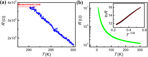
Upon heating to the deposition temperature of 800 ∘C, the surface termination of a LAO substrate will experience a transition from a Al-O layer at room temperature to a La-O layer possibly due to the creation of surface oxygen deficiencies during heating.24 Therefore, the (LaO)-(TiO2) interface is expected to form in our case, which is similar to the n-type interface as in the typical 2DEG LAO/STO heterostructure.12 Subsequently, the transport properties of both the 10 and 25 uc STO samples were examined by simple four-probe linear DC resistance measurements with a typical distance between voltage electrodes 1 mm. The samples were contacted using Al wires and the measuring current was 5 nA. Nevertheless, it was found that both samples are highly insulating with a resistance on the order of G at room temperature, in contrast to the metallicity of 2DEG observed in the case of n-type LAO/STO interface. The temperature dependence of resistance (R-T) for the 25 uc STO sample is shown in Fig. 3(a), which shows a characteristic behavior of insulators.
Microscopically the internal atomic layers of a LAO single crystal, i.e., AlO2- and LaO-layers, are polar, but the surface of a bulk LAO single crystal would likely experience surface reconstruction to be nonpolar. Thus, the growth of STO films on LAO substrates can be explained by a scenario that a nonpolar material is growing on another nonpolar surface. Therefore, the nonexistence of polar discontinuity at the interface between STO films and LAO substrates could be responsible for the highly insulating behavior. On the other hand, the epitaxial interface strain for STO films grown on LAO substrates works in the opposite direction compared to the case of LAO films grown on STO substrates, which could also affect the interface conductivity and hence account for the highly insulating behavior. However, the nanoscale intermixing of the interface atoms13 seems not suitable to clarify the highly insulating behavior here.
To investigate the effect of oxygen vacancies in the STO film on the transport properties of this heterostructure, the 25 uc STO sample was thermally reduced in a vacuum of 4 10-7 mbar at 950 ∘C for 1 h. The resistance measurement was then performed with the same measurement geometry as for Fig. 3(a). The R-T curve from 300 to 10 K as shown on a semi-logarithmic scale in Fig. 3(b) still represents an insulating behavior although the room temperature resistance decreases by nearly four orders of magnitude relative to the initial resistance (after the reduction, the LAO substrate was still extremely high insulating, which was checked from the backside of the crystal). The room temperature Hall measurement displays that the areal carrier density is cm-2, which is two orders of magnitude smaller than the ideal areal carrier density of 2DEG induced by the interface charge transfer, i.e., cm-2. Furthermore, it was found that the R-T curve can be well fitted by the variable-range hopping of Mott law, i.e., R , over the whole temperature range as plotted in the inset of Fig. 3(b), which reveals that the R-T curve belongs to the three dimensional transport property. Hence considering the thickness of 25 uc STO, the areal carrier density is converted into a volume density to be cm-3. The value is smaller than the experimental Mott critical carrier density cm-3 (Ref. 23) of the metal-insulator transition for a reduced STO film, so this can also explain why the film is still insulating even after high temperature vacuum annealing.
However, the insulating behavior in reduced STO thin films is completely different from those of reduced thicker films and bulk crystals, which show metal-insulator transition and metallicity, respectively 24. This could be due to the compensating defects like Ti vacancies and Sr vacancies dominant in ultrathin STO films, which are likely created in the high temperature and high vacuum reduction process.
Not only can STO films be layer-by-layer grown on a fully-terminated LAO substrate, the high quality atomically flat growth can also be obtained for some other perovskite materials like NdAlO3 and PrAlO3. This demonstrates an approach to achieve atomically flat interfaces based on LAO substrates, which are robust and nearly free of oxygen-vacancy-induced conductivity.
In summary, we demonstrated atomically flat interfaces between STO films and single-terminated LAO substrates. The transport measurements displayed that this type of interface is highly insulating and remains insulating even after 1 hour vacuum reduction. The reason for that could be the surface reconstruction of LAO single crystals or due to the interface epitaxial strain. This work can provide a fundamental perspective for the oxide electronics community. Besides, our work opens a way to achieve atomically flat film growth based on LAO substrates. Furthermore, the quasi-2DEG could even also be tailored probably by means of vacuum reduction or Argon-ion milling after the realization of atomically flat nanoscale film growth on LAO substrates.
Acknowledgements.
We thank M. Huijben and J. Mannhart for discussions and the National Research Foundation (NRF) Singapore under the Competitive Research Programme ‘Tailoring Oxide Electronics by Atomic Control’, NUS cross-faculty grant and FRC for financial support.References
- (1) A. Ohtomo and H. Y. Hwang, Nature (London) 427, 423 (2004).
- (2) M. Huijben, et al., Nature Mater. 5, 556 (2006).
- (3) S. Thiel, G. Hammerl, A. Schmehl, C. W. Schneider, and J. Mannhart, Science 313, 1942 (2006).
- (4) A. Brinkman, et al., Nature Mater. 6, 493 (2007).
- (5) N. Reyren, et al., Science 317, 1196 (2007).
- (6) L. Li, et al., Science 332, 825 (2011).
- (7) Ariando, et al., Nature Commun. 2, 188 (2011).
- (8) D. A. Dikin, et al., arXiv: 1103.4006.
- (9) L. Li, C. Richter, J. Mannhart, and R. C. Ashoori, arXiv: 1105.0235.
- (10) N. Pavlenko, T. Kopp, E. Y. Tsymbal, G. A. Sawatzky, and J. Mannhart, arXiv: 1105.1163.
- (11) J. W. Park, et al., Nature Commun. 1, 94 (2010).
- (12) N. Nakagawa, H. Y. Hwang, and D. A. Muller, Nature Mater. 5, 204 (2006).
- (13) P. R. Willmott, et al., Phys. Rev. Lett. 99, 155502 (2007).
- (14) J. Son, et al., Nature. Mater. 9, 482 (2010).
- (15) J. N. Eckstein, Nature Mater. 6, 473 (2007).
- (16) A. Kalabukhov, et al., Phys. Rev. B 75, 121404(R) 2007.
- (17) K. Shibuya, T. Ohnishi, M. Lippmaa, and M. Oshima, Appl. Phys. Lett. 91, 232106 (2007).
- (18) O. N. Tufte and P. W. Chapman, Phys. Rev. 155, 796 (1967).
- (19) H. W. Jang, et al., Science 331, 886 (2011).
- (20) M. Kawasaki, et al., Science 266,1540 (1994).
- (21) K. I. Nomura, et al., Japan. J. Appl. Phys. 50, 021502 (2011).
- (22) Z. Q. Liu, et al., Phys. Rev. B 84, 165106 (2011).
- (23) Z. Q. Liu, et al., Phys. Rev. Lett. 107, 146802 (2011).
- (24) J. Yao, P. B. Merrill, S. S. Perry, D. Marton, and J. W. Rabalais, J. Chem. Phys. 108, 1645 (1998).
- (25) Z. L. Wang and A. J. Shapiro, Surf. Sci. 328, 141 (1995).