Version: March 19, 2024
Epitaxial (111) Films of Cu, Ni, and CuxNiy on Al2O3(0001) for Graphene Growth by Chemical Vapor Deposition
Abstract
Films of (111)-textured Cu, Ni, and CuxNiy were evaluated as substrates for chemical vapor deposition of graphene. A metal thickness of to was sputtered onto a substrate of Al2O3(0001) at temperatures of to . The films were then annealed at in a tube furnace. X-ray and electron backscatter diffraction measurements showed all films have (111) texture but have grains with in-plane orientations differing by . The in-plane epitaxial relationship for all films was ||. Reactive sputtering of Al in O2 before metal deposition resulted in a single in-plane orientation over 97 % of the Ni film but had no significant effect on the Cu grain structure. Transmission electron microscopy showed a clean Ni/Al2O3 interface, confirmed the epitaxial relationship, and showed that formation of the twin grains was associated with features on the Al2O3 surface. Increasing total pressure and Cu vapor pressure during annealing decreased the roughness of Cu and and CuxNiy films. Graphene grown on the Ni(111) films was more uniform than that grown on polycrystalline Ni/SiO2 films, but still showed thickness variations on a much smaller length scale than the distance between grains.
1 Introduction
Uniform growth of graphene over wafer-scale areas is a critical enabling step for the commercial realization of various electronic, photonic, mechanical, and other devices based upon the superlative properties of graphene [1]. Considerable progress has been made in the growth of monolayer and few-layer graphene by chemical vapor deposition (CVD) on transition metals, particularly Cu and Ni [2, 3]. Typically, the metal surface is heated to and exposed to a hydrocarbon gas such as methane that decomposes catalytically to provide a source of C atoms on the surface. In the case of Cu, growth occurs almost entirely on the surface and is limited to a single layer for a wide range of hydrocarbon partial pressure. In the case of Ni, growth involves C dissolution into the film at high temperature and then precipitation to the surface as the film cools, which can result in both monolayer and multilayer graphene [4]. Alloys of Cu and Ni offer control over graphene thickness by adjusting the C solubility in the film [5]. The Cu or Ni can be etched away to transfer the graphene layer to an insulating substrate for further device fabrication steps [6].
Commercially available polycrystalline foils of Cu and Ni are commonly used for CVD growth of graphene because they can be annealed to have millimeter grain sizes. The best CVD graphene films to date, in terms of graphene grain size and carrier mobility, have been achieved on foils [7], but single crystal films offer several advantages. First, the hexagonal symmetry and small lattice mismatch of the (111) surface should provide a more ideal template for graphene growth than the (100), (110), or higher index surfaces. This idea is supported by recent experiments showing less rotational disorder in graphene grown on Cu(111) than on Cu(100) [8, 9]. Second, films typically provide a much smoother growth surface because foils have roughness due to the rolling process that is not fully removed by annealing. The experiments in [9] show how surface defects on Cu(111) can cause rotational disorder either at nucleation or during subsequent growth of graphene islands. Third, the diffusion of C into and out of Ni is different at grain boundaries than in the interior of grains, so better growth control and better uniformity are expected if grain boundaries are eliminated [10, 11]. Lastly, films are supported by a flat, rigid substrate, helping to simplify the process of graphene transfer to other materials. Thus we anticipate that high quality Cu(111) and Ni(111) films will enable CVD growth of graphene having improved properties compared to graphene grown on polycrystalline foils.
A suitable substrate for the metal films must, at a minimum, promote epitaxial growth with (111) texture and be physically and chemically stable under graphene CVD conditions. For wafer-scale production of graphene, the substrate should be commercially available in wafer form at a reasonable cost. The ability to reuse substrate wafers after metal etching to release the graphene layer is also desirable. Currently, the material that appears to best satisfy these requirements is Al2O3(0001), which is widely used by manufacturers of radio-frequency electronics and light-emitting diodes in the form of wafers with diameters up to . Given the advantages of single crystal Cu(111) and Ni(111) films described above, achieving such films on Al2O3 is an important step toward commercial graphene devices.
Previous investigations of Cu deposited on Al2O3(0001), mainly in ultra-high vacuum environments, found a variety of growth behaviors depending on how the Al2O3 surface was prepared. Kelber et al. [12] summarized several earlier results, discussed them in terms of multiple Al2O3(0001) surface terminations and multiple Cu ionization states, and emphasized the role of a hydroxyl layer bonded to the Al2O3 surface. The last point is particularly relevant for the work presented here. When Al2O3 is exposed to ambient air, water decomposes to form a hydroxyl (OH) layer [13] that is difficult to remove. While bombardment with 200 eV to 1000 eV Ar ions can remove all but of OH, annealing in O2 at temperatures is required to recrystallize the damaged surface [14, 15]. In typical film deposition chambers where such treatments are not available, an OH layer is likely present on Al2O3 substrates and may interfere with epitaxial growth. This may be why previous Cu films deposited on Al2O3(0001) [16, 17, 18] were not single crystals but consisted of (111) grains having in-plane orientations differing by . While Ni on Al2O3(0001) has not been the subject of extensive experimental studies, the OH layer can also be expected to interfere with epitaxy in this case. As with Cu, previous Ni films on Al2O3(0001) showed in-plane orientations differing by [11].
Epitaxy and film adhesion are relevant to graphene growth for several reasons. For Cu, which has a bulk melting point of , evaporation can cause roughness or even complete loss of the Cu film [19]. Previous work on Cu [18] showed that epitaxial and highly textured films with large grains survive graphene CVD conditions better than polycrystalline films with small grains. Ni evaporation under growth conditions is negligible, since the bulk melting point is , but Ni films can be damaged by the annealing in H2 which typically precedes graphene growth [20]. An additional consideration for Ni is that films thinner than are desirable in order to limit the total amount of C that is available to precipitate to the surface, since of Ni at can absorb enough C to form a monolayer [21]. Such thin Ni films, even when epitaxial and highly textured, can be damaged by graphene CVD conditions [11]. Given the various factors summarized here, the properties and limitations of Cu and Ni films must be considered, alongside the kinetics and thermodynamics of graphene formation from a hydrocarbon precursor, when optimizing a recipe for graphene growth by CVD.
This paper reports a study of sputtered Cu, Ni, and Cu/Ni films that have been exposed to typical graphene CVD conditions. We used x-ray diffraction (XRD) and electron backscatter diffraction (EBSD) to measure crystallinity, atomic force microscopy (AFM) to measure surface morphology, transmission electron microscopy (TEM) to image the metal/substrate interface, and optical microscopy to show film properties over large areas. We also report results for graphene growth by CVD on these films, characterized by scanning electron microscopy (SEM) and Raman spectroscopy.
2 Film Preparation
Wafers of -Al2O3(0001) were prepared by annealing at in O2 at atmospheric pressure for 24 h to remove scratches due to polishing and give atomically flat terraces. Chips of were cleaned by ultrasonic agitation in acetone and isopropanol, mounted on a resistively heated Cu puck, and placed in a cryopumped vacuum system with a base pressure below . Metal films were deposited by dc magnetron sputtering from 76 mm targets of 99.99+ % Cu or Ni in of Ar. Sputtering powers between and , corresponding to deposition rates calibrated using a profilometer of to , produced no significant differences in film properties. For some films, a “seed layer” of Al2O3 was deposited immediately before the metal by reactive sputtering from a 76 mm target of 99.999 % Al in a mixture of 40 % O2 in Ar (both 99.999 %) at a total pressure of and a power of . The target-to-substrate distance in all cases was 10 cm.
The use of a reactively sputtered seed layer to improve film adhesion and epitaxy was motivated by a desire to remove OH without using ion bombardment and high temperature annealling. Sputtering with high O2 content causes “resputtering” of the substrate due to bombardment by O– ions generated at the target and accelerated across the plasma sheath [22]. This results in a low net deposition rate, in our case, and should remove the OH layer from the substrate. The TEM results discussed below show that the reactive sputtering did not damage the surface. For the films reported here, this step was done at a substrate temperature of to promote crystallinity, but the technique was also successful at .
Metal film properties were strongly influenced by the substrate temperature during sputtering. The deposition temperature reported here was measured using a thermocouple clamped to the side of the puck facing away from the sputter gun. For fixed and without a seed layer, the films did not adhere to the Al2O3 substrate above for Cu and for Ni. Most films reported here were deposited at for Cu and for Ni. Cu/Ni bilayer films were formed by depositing of Ni and then of Cu. These films formed a homogeneous alloy upon annealing (see below) and we refer to them as “Cu-Ni” in the rest of the paper. When the Al2O3 seed layer was used, better film adhesion allowed higher . These films were deposited using a linear ramp of during deposition, from to for Cu and from to for Ni.
In order to evaluate survivability, the films were annealed in a hot-wall tube furnace before characterization. The annealing conditions were similar to those used for graphene CVD, but without the hydrocarbon precursor: duration 10 min to 15 min, temperature of , flowing 5 % H2 in Ar at a total pressure of to ( to ). The temperature of the furnace was measured using a thermocouple mounted just outside the quartz tube.
3 Film Characterization
The overall crystalline structure of the films without a seed layer, as characterized by XRD using Cu radiation with a spot size of several mm2, is shown in Fig. 1. The curves in Fig. 1a, with intensity plotted on a logarithmic scale, show a peak at from the Al2O3(0001) substrate and a peak corresponding to (111) orientation of the metal film. These peaks are located at for Cu, for Cu-Ni, and for Ni. The peaks between and are higher-order reflections, and the lack of any other peaks indicates all films are exclusively (111) textured. The rocking curves in Fig. 1b were fit with a gaussian function, yielding a full-width-at-half-maximum of 0.334° for Cu, 0.533° for Cu-Ni, and 0.393° for Ni. The single peak observed for the Cu-Ni alloy film indicates complete mixing of the two metals during annealing. Its position corresponds to an alloy composition of Cu70Ni30, whereas the Cu and Ni film thicknesses predict a composition of Cu87Ni13. We attribute this difference to the preferential evaporation of Cu during annealing.
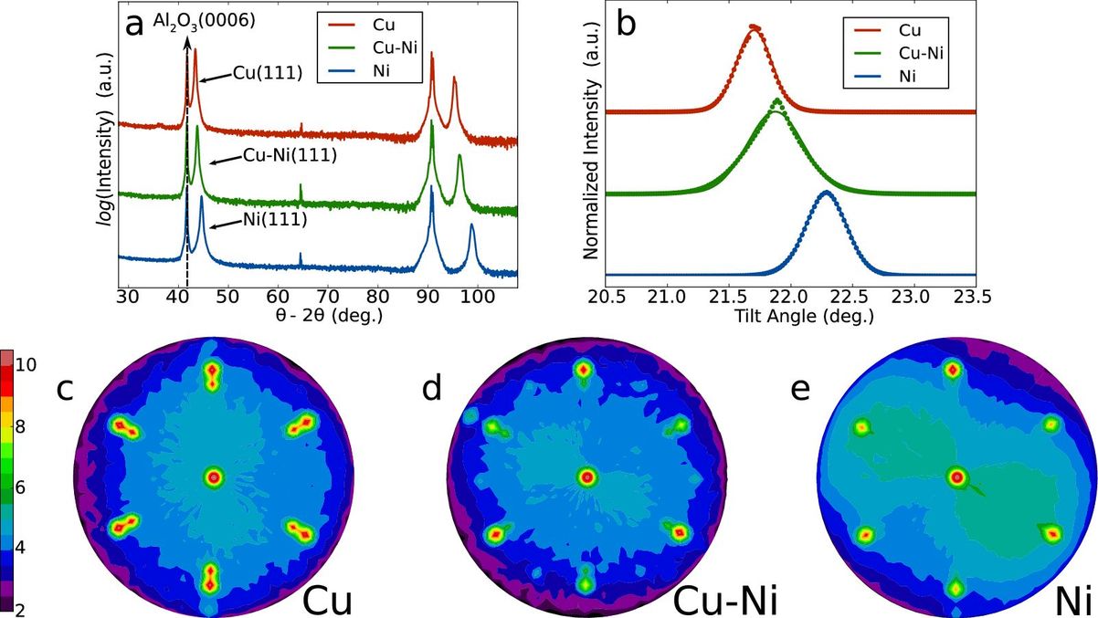
Figures 1c, d, and e show pole figures measured at the peak of the (111) reflection and plotted on a logarithmic color scale. In each pole figure, the six innermost spots come from the substrate, the other spots come from the metal film, and the rotational alignment of the two sets of spots indicates the film is epitaxially aligned with the substrate. The measured epitaxial relationship for all films can be expressed as || and ||, consistent with prior results for several fcc metals on Al2O3 [23]. For a (111) film with a single in-plane orientation, the pole figure would show only three spots. The six spots with similar intensity shown in Fig. 1c indicate roughly half the Cu film is rotated in-plane by with respect to the rest of the film. The second set of spots appears with lower intensity in Figs. 1c, d, indicating that only a minority of the Cu-Ni and Ni films are rotated by . Comparing the integrated intensities for the two sets of spots, we estimate the fraction of the film composed of these twin domains to be 50 % for Cu, 15 % for Cu-Ni, and 25 % for Ni. The Cu-Ni film also shows faint spots in between the six stronger spots, indicating that a small minority (< 1 %) of the film is rotated in-plane by 30°. Overall, the XRD characterization shows that all films are (111) textured but have some degree of in-plane rotational disorder. This is not unexpected because there are two equivalent orientations for a cubic film deposited on a hexagonal substrate.
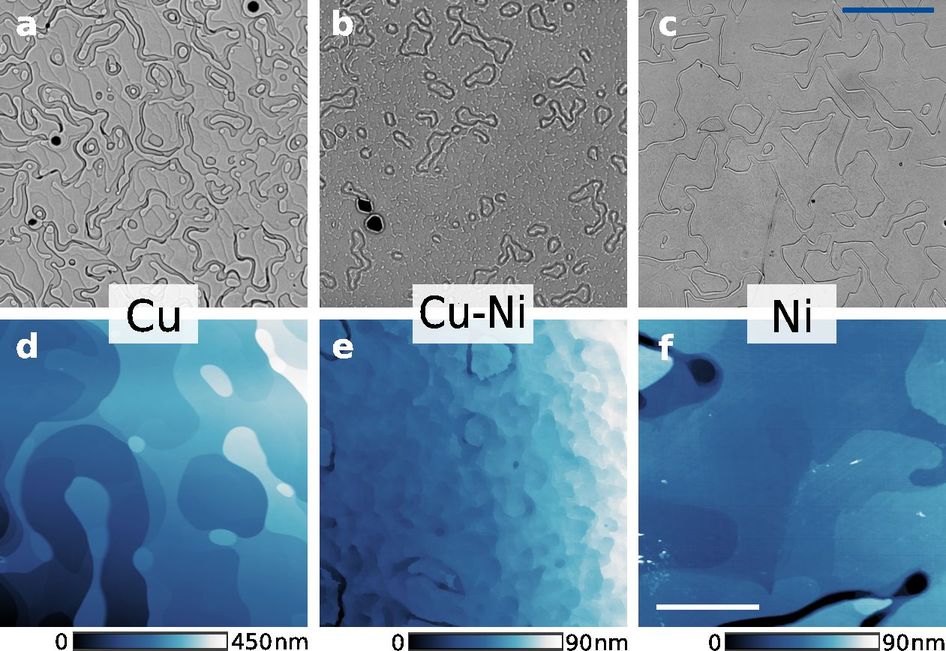
The morphology of the films without a seed layer is shown in Fig. 2. The Cu film shows a rough surface in both optical and AFM images. The black spots in the optical image are areas of the film that have dewetted from the substrate, and these spots increase in size and density for longer annealing times. Both the roughness and the dewetting indicate the Cu film is only marginally stable at . Such instability has been noted previously [24, 19] and can be attributed to the rapid evaporation of Cu when heated near its bulk melting temperature in rough vacuum. This is discussed further below. The Cu-Ni film is smoother than the Cu film and shows a lower density of dewetting spots. The Ni film is smoothest of all and has the fewest dewetting spots. The AFM image of the Ni shows areas of several that are atomically smooth (rms roughness to for a area). The EBSD characterization discussed below suggests that the dark lines in the optical images for Cu-Ni and Ni are boundaries between the twin domains revealed in the XRD data. These grain boundaries are wider for the Cu-Ni film than for the Ni film, and are obscured by roughness for the Cu film. In the AFM images for Cu-Ni and Ni, the grain boundaries appear as trenches. These trenches, which do not appear in the as-deposited films, likely form when grain boundaries move during annealing. These morphological characterizations show that the Ni film clearly survives the annealing better than the Cu film, as expected from the higher melting point of Ni.
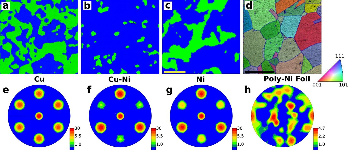
The micro-crystalline structure of the films can be characterized by EBSD, as shown in Fig. 3 for films without a seed layer. Because the films are fully (111) textured, we use a color scale for in-plane direction only: blue and green regions differ by a rotation about the [111] axis. The upper images are therefore spatial maps of the twin domains revealed in the XRD data. The lower images are (111) pole figures with a logarithmic color scale. The spatial map for the Cu film shows a broad distribution of grain sizes, and the pole figure shows equal intensity for both in-plane orientations. For the Cu-Ni film, both the spatial map and the pole figure indicate that one orientation dominates in the region shown here. Comparing the orientation map of Fig. 3b and the optical image of Fig. 2b, we conclude that the dark lines enclosing small areas in the optical image are boundaries between twin domains. A less pronounced preference for one in-plane orientation is apparent in the spatial map and pole figure of the Ni film. For comparison with our (111) films, Figs. 3d, h show EBSD data for a polycrystalline Ni foil, also annealed at . In this case we use a color scale for out-of-plane orientation. The foil shows a broad distribution of grain sizes and orientations.
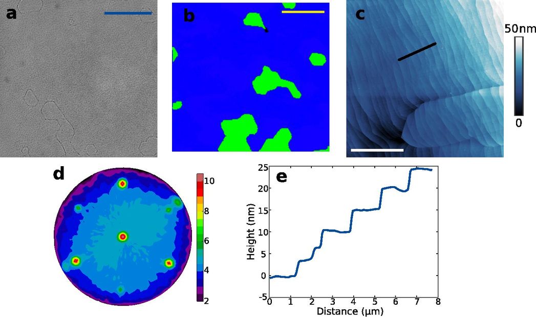
We now turn to the effect of the Al2O3 seed layer and other measures that improved the metal films in terms of epitaxy and/or survivability under graphene CVD conditions. The seed layer improved the adhesion of all films, as indicated by a reduced density of dewetting areas after annealing. For the Cu films, the seed layer had little effect on crystallinity: the XRD pole figure (not shown) has six spots of similar intensity, indicating roughly equal amounts of each twin orientation, as in the data of Fig. 1c. For the Ni films, the seed layer increased grain size and reduced twin formation, as shown in Fig. 4. The second set of spots in the XRD pole figure of Fig. 4d is faint even on a logarithmic scale, and from their integrated intensity we estimate that only 3 % of the film area is composed of twin domains. The optical image in Fig. 4a shows fewer lines due to grain boundaries, and the lines are less distinct than in Fig. 2c. Finally, the AFM image in Fig. 4c shows the detailed morphology of the improved Ni film. The surface shows a regular series of atomically flat terraces, also seen in the profile of Fig. 4e, that are wide and separated by steps tall. This profile corresponds to a slope of 0.3°, consistent with the miscut specification of the Al2O3 wafer. The trenches between twin domains are shallower than for Ni without the seed layer, which is consistent with less grain boundary motion during annealing due to the higher deposition temperature.
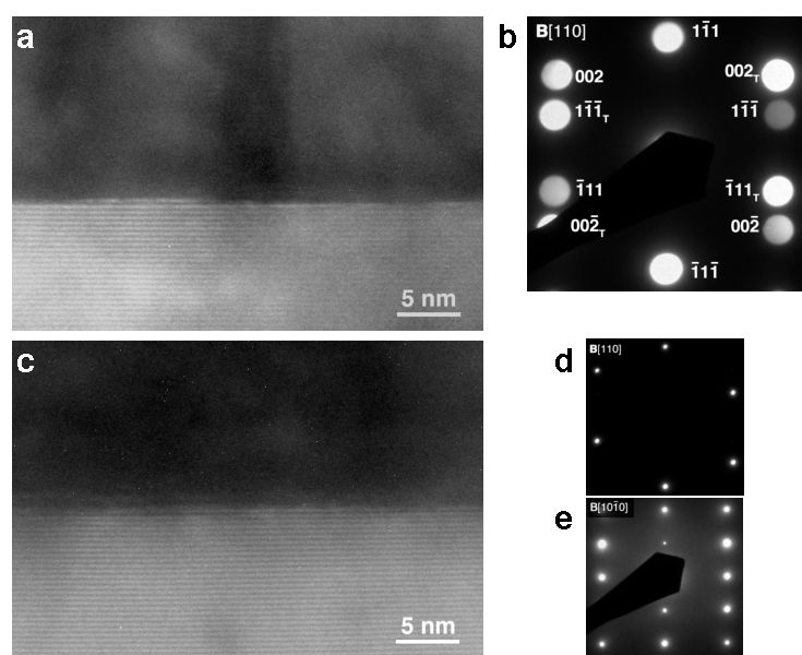
To further investigate the effect of the seed layer, TEM was performed on a cross-section of the Ni/Al2O3 interface from unannealed samples with and without the seed layer. The bottom half of each image in Figs. 5a,c shows Al2O3(0003) lattice fringes, which are kinematically forbidden but dynamically allowed and are observed due to double diffraction. Ni lattice fringes are not resolved because the distance between Ni(111) planes, 0.203 nm, is beyond the 0.28 nm point resolution of the microscope. For the Ni film without the seed layer, Fig. 5a, the last Al2O3 fringe shows a lateral intensity modulation that could indicate a fractional-unit-cell island or dislocation near the surface. At the edge of the extra fringe, there is a vertical grain boundary in the Ni (darker region near the center of the image). The focused probe diffraction pattern corresponding to this region, shown in Fig. 5b, indicates both grains share the [111] out-of-plane and [110] in-plane directions. This can only occur for a twin boundary with a in-plane rotation about the [111] direction. The presence of a Ni grain boundary at the edge of an extra (0003) Al2O3 lattice fringe was not uncommon, so the extra fringe is likely correlated with the mechanism for grain boundary formation. Thus the TEM results independently confirm the EBSD results and provide a microscopic view of the origin of the twin domains.
For the Ni film grown with the seed layer, we found far fewer grain boundaries for an equivalent length of cross-sectional interface. Fig. 5c shows a typical image for this film. The Al2O3 lattice fringes are continuous and smooth, indicating the reactive sputtering produced a seed layer with an undamaged surface. Selected area electron diffraction patterns show the Ni (Fig. 5d) and the Al2O3 (Fig. 5e) are highly ordered.
While the Al2O3 seed layer did not significantly affect the amount of twin domains or other properties of the Cu films, the roughness of these films was strongly affected by the annealing conditions. The rough surface shown in Fig. 2a, produced by annealing for 15 min at in a total pressure of (), offers a poor substrate for graphene growth. Increasing the total pressure during annealing reduced the overall roughness of Cu and Cu-Ni films, as shown in Table 1. We attribute this improvement to the reduced evaporation rate of Cu at higher pressure. Table 1 also shows that roughness was further decreased by placing a Cu foil above the surface of the Cu film. This improvement is presumably due to a higher vapor pressure of Cu near the film, and is likely related to the improvements seen in graphene CVD when the Cu foil was folded and crimped to make an enclosure [25]. With both higher total pressure and a foil cover, a Cu(111) film annealed at for 15 min showed a roughness only slightly larger than that of the Ni film in Fig. 4c. Thus thin Cu(111) films on Al2O3 can survive graphene CVD conditions, even those approaching the Cu melting point, if the total pressure is high enough and there is a nearby source of Cu vapor.
| Film | Thickness (nm) | Temp. () | Press. (Torr) | Foil cover | Roughness (nm) |
|---|---|---|---|---|---|
| Cu | 400 | 1000 | 2 | No | 27 |
| Cu | 700 | 1000 | 20 | No | 9.5 |
| Cu | 700 | 1000 | 40 | No | 6.8 |
| Cu | 700 | 1000 | 20 | Yes | 5.8 |
| Cu | 700 | 1065 | 40 | Yes | 5.0 |
| Cu-Ni | 350/50 | 1000 | 2 | No | 18 |
| Cu-Ni | 350/50 | 1000 | 20 | No | 13 |
| Ni | 400 | 1000 | 2 | No | 3.3 |
4 Graphene Growth and Characterization
Graphene was grown using CH4 as the precursor gas in a hot-wall tube furnace with an inner diameter of 80 mm and an overall length of 1.5 m. The tube was evacuated using a scroll pump (base pressure of ) and all gases were 99.99+ % pure. For growth on Ni, the films were annealed at in a flow of () of Ar and of H2 for 15 min, cooled to , and then exposed to of H2 and of CH4. Growth conditions were maintained for 30 min to ensure full C saturation, and the film was cooled at in the same gas flows used for growth. A total pressure of () was maintained throughout the process. For growth on Cu, the films were annealed at in () of Ar and () of H2 for 15 min. A flow of () of CH4 was then added to the Ar and H2, growth lasted 4 min, and the film was cooled at approximately in the same gas flows used for growth. A total pressure of () was maintained throughout the process.
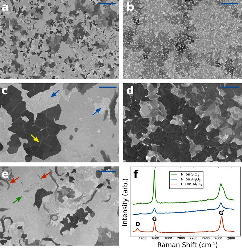
Scanning electron microscopy (SEM) at low accelerating voltage (5 kV) was used to image graphene on the Ni and Cu surfaces. Figure 6 compares growth on films of epitaxial Ni(111) on Al2O3 (Fig. 6a,c,e) and polycrystalline Ni on SiO2 (Fig. 6b,d). The graphene films were grown simultaneously to ensure identical treatment. We attribute variations in the grey-scale to variations in graphene thickness, with darker areas presumably corresponding to thicker graphene. Although contrast variations from the polycrystalline Ni film itself could exist due to channeling, we expect this effect to be minimal because the images were taken with an in-lens detector. The most striking feature in these images is the different relationship between graphene thickness changes and Ni grain boundaries for the two films. For the polycrystalline Ni film, most changes in thickness occur at grain boundaries, leading to mostly faceted edges for regions of a given thickness (Fig. 6d). For the Ni(111) film, the graphene thickness varies dramatically on a length scale much smaller than the size of the grains shown in the EBSD data of Fig. 4b. Thus while graphene growth on Ni(111) is indeed more uniform than growth on polycrystalline Ni, it is not nearly as uniform as one would expect if thickness variations are simply caused by faster precipitation of C at grain boundaries than within the interior of grains. This suggests there is an additional source of thickness variations that remains to be identified. Similar thickness variations occured for a variety of growth parameters.
The higher resolution SEM images in Fig. 6c,e show detailed features of the thickness variations that are worth mentioning. In some places, thicker graphene follows the boundary between a minority grain and the surrounding majority grain (red arrows in Fig. 6e). This has been reported previously for growth on Ni [11] and is likely due either to faster precipitation of C or to trapping of C atoms at these boundaries. In other places, the boundaries of minority grains have no change in graphene thickness (green arrow in Fig. 6e). In many of the thicker graphene regions, straight, bright lines may indicate buckling of the graphene from differential contraction during cooling (yellow arrow in Fig. 6c). Some of the thinnest graphene regions show a network of bright lines that may indicate a discontinuous mosaic of graphene patches (blue arrows in Fig. 6c). The variety of growth features on a substrate of such high quality highlights the need for a better understanding of how graphene grows on Ni.
Raman spectroscopy using an excitation wavelength of 633 nm was done to verify the existence of graphene and as a rough characterization of defects. The thickest graphene ( layers) on Ni films appears darker in an optical microscope. Raman spectra with a spot size of were taken in between these darker patches to preferentially sample the thinnest regions. Fig. 6f shows typical spectra, which have the G and G’ peaks characteristic of few-layer graphene [26]. No places were found that did not have these peaks, indicating the films were fully covered by graphene. The lack of a significant D peak in the Raman spectra for graphene on Ni indicates there are few defects.
The graphene grown on Cu is primarily monolayer, as shown by the Raman spectrum in Fig. 6e, and therefore SEM images (not shown) reveal little about the growth. The large D peak is likely due to a high density of graphene nucleation sites, resulting in a large number of graphene grain boundaries. When graphene growth is interrupted before a complete layer forms, the nucleation sites can be seen directly in SEM images [7]. Nucleation sites were separated by roughly , much less than the distance between Cu grain boundaries in Fig. 3a. As with Cu foils [7], we expect that optimization of growth conditions can improve the quality of graphene on Cu(111) films.
5 Conclusion
The metal films reported here have many of the properties needed for wafer-scale growth of graphene by CVD. They can be deposited epitaxially with a pure (111) texture on commercially available Al2O3(0001) substrates. The films fall short of being single crystals only due to grain boundaries between (111) regions that differ by an in-plane rotation of . For Ni, a film that is 97 % single orientation and has a smooth, well ordered surface can be achieved by reactive sputtering of an Al2O3 seed layer immediately before metal deposition. This process, which probably helps by removing the OH layer typically found on Al2O3 after exposure to air, does not require ion bombardment or temperatures above and thus can be implemented in many commercial sputtering systems if they are fitted with a basic substrate heater. Cu films do not show significant improvement from the seed layer process, but the roughness of these films caused by evaporation under graphene CVD conditions can be reduced by a combination of higher total pressure and proximity of a Cu foil. Cu-Ni films deposited as bilayers become homogeneous alloys when annealed at , demonstrating the possibility of tuning C solubility through alloy composition and thereby controlling graphene thickness. The evaporation of Cu during annealing can have a significant effect on the final alloy composition.
Further improvements are needed to reach the goal of wafer-scale, single crystal thin films of Cu, Ni, and Cu-Ni alloys. Optimization of the reactive sputtering process and the use of a sputtering system with lower base pressure may result in fewer grain boundaries than demonstrated here. The improvements found in the Ni films may be transferable to Cu films through the use of a few nanometers of Ni deposited before the Cu. Another possible route is the use of MgO substrates. In recent work, both Cu [27] and Ni [28] deposited on MgO(111) showed a (111) texture without apparent in-plane rotational disorder, and the films did not noticeably degrade under graphene CVD conditions. These measurements may have been less sensitive to in-plane rotations than the XRD pole figures presented here, but if these films do contain a small fraction that is rotated in-plane, they may also benefit from a reactively sputtered seed layer. Unfortunately, wafers of crystalline MgO are not widely available.
Independent of progress on film quality, there is clearly room for improvement in our understanding of graphene CVD on metal substrates, be they foils, films or ingots. The work presented here implies that even a single crystal metal film free of grain boundaries may not be sufficient to achieve the graphene uniformity needed for commercial applications. The identification of other mechanisms for graphene nonuniformity remains an important topic of research.
6 Acknowledgments
We thank Dustin Hite and David Pappas for advice on metal film growth, Lawrence Robins and Angela Hight-Walker for assistance with Raman spectroscopy, and Stephen Russek for helpful discussions about magnetron sputtering.
References
References
- [1] Phaedon Avouris. Graphene: Electronic and photonic properties and devices. Nano Lett., 10:4285–4294, 2010.
- [2] Matthias Batzill. The surface science of graphene: Metal interfaces, CVD synthesis, nanoribbons, chemical modifications, and defects. Surf. Sci. Reports, 67:83 – 115, 2012.
- [3] Cecilia Mattevi, Hokwon Kim, and Manish Chhowalla. A review of chemical vapour deposition of graphene on copper. J. Mater. Chem., 21:3324–3334, 2011.
- [4] Alfonso Reina, Stefan Thiele, Xiaoting Jia, Sreekar Bhaviripudi, Mildred Dresselhaus, Juergen Schaefer, and Jing Kong. Growth of large-area single- and bi-layer graphene by controlled carbon precipitation on polycrystalline Ni surfaces. Nano Research, 2:509–516, 2009.
- [5] Xun Liu, Lei Fu, Nan Liu, Teng Gao, Yanfeng Zhang, Lei Liao, and Zhongfan Liu. Segregation growth of graphene on Cu–Ni alloy for precise layer control. J. Phys. Chem. C, 115:11976–11982, 2011.
- [6] Ji Won Suk, Alexander Kitt, Carl W. Magnuson, Yufeng Hao, Samir Ahmed, Jinho An, Anna K. Swan, Bennett B. Goldberg, and Rodney S. Ruoff. Transfer of CVD-grown monolayer graphene onto arbitrary substrates. ACS Nano, 5:6916–6924, 2011.
- [7] Xuesong Li, Carl W. Magnuson, Archana Venugopal, Jinho An, Ji Won Suk, Boyang Han, Mark Borysiak, Weiwei Cai, Aruna Velamakanni, Yanwu Zhu, Lianfeng Fu, Eric M. Vogel, Edgar Voelkl, Luigi Colombo, and Rodney S. Ruoff. Graphene films with large domain size by a two-step chemical vapor deposition process. Nano Lett., 10:4328–4334, 2010.
- [8] Joseph M. Wofford, Shu Nie, Kevin F. McCarty, Norman C. Bartelt, and Oscar D. Dubon. Graphene islands on Cu foils: The interplay between shape, orientation, and defects. Nano Lett., 10:4890–4896, 2010.
- [9] Shu Nie, Joseph M. Wofford, Norman C. Bartelt, Oscar D. Dubon, and Kevin F. McCarty. Origin of the mosaicity in graphene grown on Cu(111). Phys. Rev. B, 84:155425, 2011.
- [10] Yi Zhang, Lewis Gomez, Fumiaki N. Ishikawa, Anuj Madaria, Koungmin Ryu, Chuan Wang, Alexander Badmaev, and Chongwu Zhou. Comparison of graphene growth on single-crystalline and polycrystalline Ni by chemical vapor deposition. J. Phys. Chem. Lett., 1(20):3101–3107, 2010.
- [11] Shigeo Yoshii, Katsuya Nozawa, Kenji Toyoda, Nozomu Matsukawa, Akihiro Odagawa, and Ayumu Tsujimura. Suppression of inhomogeneous segregation in graphene growth on epitaxial metal films. Nano Lett., 11:2628–2633, 2011.
- [12] J.A. Kelber, Chengyu Niu, K. Shepherd, D.R. Jennison, and A. Bogicevic. Copper wetting of Al2O3(0001): theory and experiment. Surf. Sci., 446:76 – 88, 2000.
- [13] Peter J. Eng, Thomas P. Trainor, Gordon E. Brown Jr., Glenn A. Waychunas, Matthew Newville, Stephen R. Sutton, and Mark L. Rivers. Structure of the hydrated -Al2O3 (0001) surface. Science, 288(5468):1029–1033, 2000.
- [14] Sang Ho Oh, Christina Scheu, Thomas Wagner, Elena Tchernychova, and Manfred Rühle. Epitaxy and bonding of Cu films on oxygen-terminated -Al2O3(0 0 0 1) surfaces. Acta Materialia, 54:2685 – 2696, 2006.
- [15] C. Scheu, M. Gao, S. Oh, G. Dehm, S. Klein, A. Tomsia, and M. Rühle. Bonding at copper–alumina interfaces established by different surface treatments: a critical review. J. Mater. Sci., 41:5161–5168, 2006.
- [16] Kongara M. Reddy, Andrew D. Gledhill, Chun-Hu Chen, Julie M. Drexler, and Nitin P. Padture. High quality, transferrable graphene grown on single crystal Cu(111) thin films on basal-plane sapphire. Appl. Phys. Lett., 98:113117, 2011.
- [17] Masatou Ishihara, Yoshinori Koga, Jaeho Kim, Kazuo Tsugawa, and Masataka Hasegawa. Direct evidence of advantage of Cu(111) for graphene synthesis by using Raman mapping and electron backscatter diffraction. Mater. Lett., 65:2864 – 2867, 2011.
- [18] Baoshan Hu, Hiroki Ago, Yoshito Ito, Kenji Kawahara, Masaharu Tsuji, Eisuke Magome, Kazushi Sumitani, Noriaki Mizuta, Ken ichi Ikeda, and Seigi Mizuno. Epitaxial growth of large-area single-layer graphene over Cu(111)/sapphire by atmospheric pressure CVD. Carbon, 50:57 – 65, 2012.
- [19] Ariel Ismach, Clara Druzgalski, Samuel Penwell, Adam Schwartzberg, Maxwell Zheng, Ali Javey, Jeffrey Bokor, and Yuegang Zhang. Direct chemical vapor deposition of graphene on dielectric surfaces. Nano Lett., 10:1542–1548, 2010.
- [20] Stefan Thiele, Alfonso Reina, Paul Healey, Jakub Kedzierski, Peter Wyatt, Pei-Lan Hsu, Craig Keast, Juergen Schaefer, and Jing Kong. Engineering polycrystalline Ni films to improve thickness uniformity of the chemical-vapor-deposition-grown graphene films. Nanotechnology, 21:015601, 2010.
- [21] W. W. Dunn, R. B. McLellan, and W. A. Oates. The solubility of carbon in cobalt and nickel. Trans. Metall. Soc. AIME, 242:2129, 1968.
- [22] Daniel J. Kester and Russell Messier. Macro-effects of resputtering due to negative ion bombardment of growing thin films. J. Mater. Res., 8:1928–1937, 1993.
- [23] H Bialas and K Heneka. Epitaxy of fcc metals on dielectric substrates. Vacuum, 45:79 – 87, 1994.
- [24] Mark P. Levendorf, Carlos S. Ruiz-Vargas, Shivank Garg, and Jiwoong Park. Transfer-free batch fabrication of single layer graphene transistors. Nano Lett., 9:4479–4483, 2009.
- [25] Xuesong Li, Carl W. Magnuson, Archana Venugopal, Rudolf M. Tromp, James B. Hannon, Eric M. Vogel, Luigi Colombo, and Rodney S. Ruoff. Large-area graphene single crystals grown by low-pressure chemical vapor deposition of methane on copper. J. Amer. Chem. Soc., 133:2816–2819, 2011.
- [26] L.M. Malard, M.A. Pimenta, G. Dresselhaus, and M.S. Dresselhaus. Raman spectroscopy in graphene. Phys. Rep., 473:51 – 87, 2009.
- [27] Yui Ogawa, Baoshan Hu, Carlo M. Orofeo, Masaharu Tsuji, Ken-ichi Ikeda, Seigi Mizuno, Hiroki Hibino, and Hiroki Ago. Domain structure and boundary in single-layer graphene grown on Cu(111) and Cu(100) films. J. Phys. Chem. Lett., 3:219–226, 2012.
- [28] Takayuki Iwasaki, Hye Jin Park, Mitsuharu Konuma, Dong Su Lee, Jurgen H. Smet, and Ulrich Starke. Long-range ordered single-crystal graphene on high-quality heteroepitaxial Ni thin films grown on MgO(111). Nano Lett., 11:79–84, 2011.