Magnetodielectric effect of Graphene-PVA Nanocomposites
Abstract
Graphene-Polyvinyl alcohol (PVA) nanocomposite films with thickness were synthesized by solidification of PVA in a solution with dispersed graphene nanosheets. Electrical conductivity data were explained as arising due to hopping of carriers between localized states formed at the graphene-PVA interface. Dielectric permittivity data as a function of frequency indicated the occurrence of Debye-type relaxation mechanism. The nanocomposites showed a magnetodielectric effect with the dielectric constant changing by as the magnetic field was increased to 1 Tesla. The effect was explained as arising due to Maxwell-Wagner polarization as applied to an inhomogeneous two-dimensional,two-component composite model. This type of nanocomposite may be suitable for applications involving nanogenerators.
I Introduction
Graphene has been at the forefront of nanomaterials research in recent times geim ; novo . Apart from devising simpler and more efficient ways of synthesizing graphene sheets stankovich ; lotya ; cnrjpc ; cnrjmc ; cnrwi ; reinanl ,theoretical work has progressed at a fast pace to explain the intriguing electronic properties of graphene castro ; sds ; allor ; shytov ; young ; stander ; sui . The elucidation of quantum transport mechanism in graphene will have a strong bearing on the design of graphene based nanoscale devices. A number of investigations have been reported regarding synthesis of composites incorporating graphene sheets. Transparent and electrically conducting graphene-silica composites have been prepared and characterized watcharotonenl . Polystyrene-graphene composites formed via complete exfoliation of graphite and dispersion of resultant graphene sheets in the polymer have shown a very low percolation threshold for room temperature conductivity stankovichnat . Graphene-metal particle nanocomposites have been synthesized by first adsorbing metal particles on graphene oxide sheets which are then catalytically reduced to graphene xujpcc . An interesting development is the method of chemical storage of hydrogen in a few-layer graphene structure cnrpnas . Graphene-Polyaniline nanocomposites have been used for hydrogen gas sensing almashatjpcc .
Our objective was to investigate the electrical properties of a composite consisting of graphene sheets dispersed in a polymer matrix. Apart from the conduction mechanism we wanted to explore the possibility of inducing magnetodielectric effect in these materials because of inhomogeneous conductor microstructure within them. It was indeed possible to obtain such behaviour. The details are reported in this paper.
II Experimental
The graphene-PVA nanocomposite was synthesized by a simple chemical polymerization method. Primarily, graphene nanosheets were prepared by the chemical reduction and exfoliation of graphite oxide. The graphite oxide (GO) was prepared from high purity graphite flakes (as obtained from LOBACHEMIE) using modified Hummers’ method hummersjacs ; zhoujpcc . In brief, 2gm of powdered flake graphite was added to a mixture of 50ml concentrated sulfuric acid (,as obtained from E-Merck) 2gm and 6gm .The ingredients were mixed in a beaker that had been cooled to 273K in an ice-bath. After removing the ice-bath the temperature of the suspension was brought to room temperature under constant stirring. After 3 hrs,300ml distilled water and 5ml hydrogen peroxide() were added to the thick mixture under stirring. Finally, the suspension was filtered,resulting in a yelloish brown cake. This was washed with 1:10 HCl solution inorder to remove unwanted metal ions kovtycm . The washed product was then collected and dried in an air oven at 333K. Graphene (or more suitably reduced graphene oxide) was prepared by usual chemical reduction technique dannn . 0.01gm GO powder was uniformly dispersed in 10 ml water and 6 ml hydrazine hydrate was added. The pH of the mixture was kept at by adding ammonia solution. The mixture was stirred thoroughly at room temperature for 3 hrs to remove the oxygen functionality of the graphite oxide.
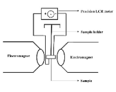
0.909 gm of poly-vinyl alcohol (PVA) powder (as obtained from S-d fine-Chem Pvt.Ltd.) was dissolved in 15 ml water and stirred at 333K for 3hrs. to form a homogeneous polymer solution. The elevated temperature was needed as PVA does not dissolve in water at room temperature (300K). It may be noted therefore that the preparation entailed GO and of PVA (by weight) as precursors. 3 ml of dispersed graphene was mixed with 10 ml PVA solution and stirred for 4 hrs. to form a homogeneous mixture. The mixture was then cast on a teflon petri-dish at ordinary atmosphere. After solidification, graphene-PVA nanocomposite film was obtained. To characterize the prepared graphene, the sample was mounted on transmission electron microscope (JEOL 2010, operated at 200 kV). Fourier Transform Infrared spectroscopy studies of both the GO and pristine graphene samples were carried out using FTIR8400S spectrometer. For electrical measurements,silver electrodes (silver paint supplied by M/S Acheson Colloiden, B.V. The Netherlands) were applied on both the faces of a piece of graphene-PVA nanocomposite film. For dc electrical resistivity measurement Keithley 617 electro meter was used,whereas, for dielectric and magnetodielectric coupling measurements, an Agilent E4890A precision LCR meter was used. In order to determine the change of dielectric constant with applied magnetic field (magnetodielectric coupling measurement) the orientation of magnetic field was kept perpendicular to the applied electric field. In this case magnetic field was generated by a large water cooled electromagnet supplied by M/S Control Systems & Devices, Mumbai,India. The schematic diagram of the experimental set-up has been shown in 1.
III Results and Discussion
The FTIR (Fourier Transform Infrared Spectroscopy) spectra of both the graphite oxide (GO) and the graphene sample has been shown in 2. The spectrum for GO shows transmittance dips at 1390.65 ,1634.23 and 1725.14 , which correspond to deformation of O-H bond in water, stretching mode of carbon carbon double bond (C=C) and stretching mode of carbon oxygen double bond (C=O) respectively.On the other hand in the spectrum for chemically derived graphene the absence of any dip around 1725 establishes that the derived graphene samples are free from the oxygen functionality present in GO.
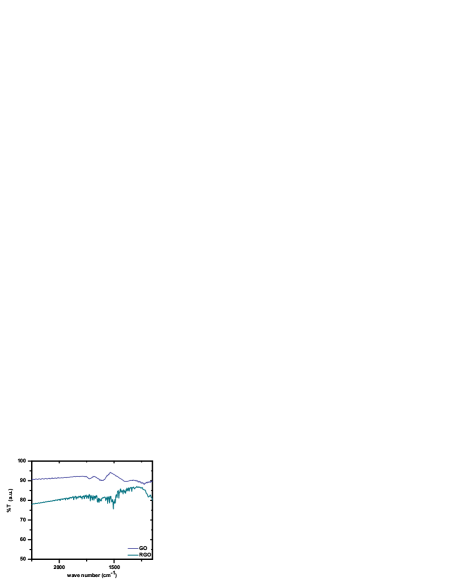
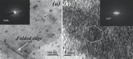
Figure 3(a) shows the low magnification transmission electron micrograph of the graphene sheet showing the morphology. The folded edge signifies that the sheet is very thin as expected, probably 4-5 layers of graphene. The selected area electron diffraction pattern of the graphene sheet is shown in the inset of figure 3(a). The high resolution transmission electron micrograph of graphene sheet showing the lattice planes, has been shown in figure 3(b). It should be evident that the lattice pattern is hexagonal in nature ,which is further substantiated by the fast fourier transform (FFT) of the image, shown as inset in figure 3(b).
The variation of logarithm of dc resistivity as a function of T-1 for the graphene-PVA nanocomposite film has been shown in 4. The silver electroded film has a thickness and area of cross-section ( and ) respectively.
From the slope of this Arrhenius plot we calculate a value of activation energy using
| (1) |
where, is the activation energy which comes out to be 0.38 eV.
The points shown in figure are the experimental points and the solid line represents the least square fitted curve.

We argue that the edges of the graphene sheets form localised states in the amorphous PVA medium and the conduction mechanism is governed by hopping of the carriers near the Fermi level between these localised states mott .The variation of the ac conductivity of the nanocomposite as a function of the angular frequency at 304K is shown in 5. We have used the formula derived by Davis and Mott, mott
| (2) |
where is the conductivity for the angular frequency , N is the density of states in the vicinity of Fermi level, kB is Boltzmann constant, T is temperature, e is the electronic charge, is the localization constant and is the inverse of phonon frequency. The experimental data in 5 were least-square fitted to eq.2 using N,,and as parameters. The theoretically fitted curve is shown in 5. The values extracted are N=1.0×10,=1.0×10⁻¹¹ sec,and =72 Ao. These values are similar to those reported for various chalcogenide glassesmott .

The dielectric permittivity of the nanocomposite film was measured and we have delineated the real and imaginary components of the same. The variation of real and imaginary parts of the dielectric permittivity with the frequency, measured at different temperatures is shown in figures 6 and 7 respectively. It can be seen that the real part decreases from a constant high value as the frequency is increased and on the contrary, the imaginary part shows a Debye-like relaxation peak hippel ,which shifts towards the higher frequency side as the temperature is increased. The graphene-PVA nanocomposite film shows dielectric dispersion, which is evident from the Cole-Cole diagram cole shown in 8. The semi-circle in the Cole-Cole plot characterizes the dielectric data.


The dielectric data can be explained on the basis of an inhomogeneous dielectric having laminar structure with different values of dielectric permittivity and electrical conductivity. It was shown previously, such systems exhibited dielectric dispersion with a single relaxation time cole ; isard which is evident from the Cole-Cole diagram. In the present case, the laminae consist of two-dimensional graphene sheets acting as conducting layer surrounded by the insulating PVA. The analysis of the dielectric data signifies that the graphene-PVA nanocomposite is electrically inhomogeneous.
From 7 the values of the relaxation times corresponding to the maximum values of at different temperatures were found out and the results are plotted in 9 as a function of T-1. The activation energy of the relaxation process was estimated according to carbon
| (3) |
where is the activation energy for the relaxation process and T is absolute temperature. From the slope of the straight line the value of the activation energy of 1.29 eV was extracted.

Our system resembles an ideal Maxwell-Wagner dielectric, for which we have investigated a possible magnetodielectric effect. This work has been motivated by a recent theoretical work littlewood . We had earlier reported this effect in case of nickel nanosheets embedded within the crystal channels of Na-4 mica selfepl . This is essentially an interface effect, in which the space charges accumulate at the interface of the conducting and non conducting layers. This causes an effective dipole moment in the system, reflected in the corresponding dielectric constant of the nanocomposite. By the application of the magnetic field,the charges move perpendicular to both the electric and magnetic field directions. The movement of these charges, causes the lowering of the space charge density and the value of dielectric constant is decreased. The dielectric permittivity of an inhomogeneous medium consisting of a purely capacitive and a purely resistive region connected in series, under magnetic field has been given by, littlewood
| (4) |
where is the effective dielectric permittivity, is angular frequency of the applied electric field, is the dielectric constant of the polymer matrix, , is the resistivity of the graphene film, and ; is the carrier mobility and H is the applied magnetic field. The variation of the real part of the dielectric permittivity of the nanocomposite film with the magnetic field has been shown in 10.


As explained above,the dielectric constant decreases with the increase in magnetic field. We have fitted the experimental data with equation (4), for different frequencies of applied electric field,and the fitting looks satisfactory for all frequencies. In the calculation, we have used geim for graphene film and for PVA url . It is worthy to note that the dielectric constant of the composite decreases with the increasing frequencies,which is a characteristic feature of the Maxwell-Wagner polarization effect hippel . The variation of the imaginary part of the dielectric constant with the magnetic field has also been shown in 11, and the solid line represents the theoretically fitted curve.
From the magnetic field dependence of the dielectric permittivity of this material one will be tempted to make use of it to probe magnetic field. However the effect is admittedly quite small for such an application to be feasible.Use as a magnetic sensor in nanocircuits could still be a possibility. On the other hand, such materials should be explored for making nano-generators viz;by applying an alternating magnetic field a sinusoidal variation of polarization (i.e. bound charge density at electrodes) could be effected. From the latter by a suitable electrical circuitry a sinusoidal voltage could be generated.Such work will be taken up in our laboratory shortly.
IV Conclusion
In summary, graphene sheets were produced by reduction and subsequent exfoliation of graphite oxide powder. PVA solution with dispersed graphene nanosheets were solidified, which led to the formation of graphene-PVA nanocomposite films of thickness 120 . Electrical conductivity of the composite was found to be caused by hopping of carriers between localised states formed at graphne-PVA interface. Dielectric dispersion data showed a Debye like relaxation mechanism. The nanocomposites exhibited magnetodielectric effect which was explained on the basis of a heterogeneous two-dimensional,two-component composite model.
Acknowledgement
Support for this work was derived from an Indo-Australian Project on nanocomposites for Clean Energy granted by Department of Science and Technology, Govt. of India, New Delhi. SM thanks University Grants Comission,New Delhi,and DRS thanks Council of Scientific and Industrial Research,New Delhi for awarding Senior Research Fellowships. DC thanks Indian National Science Academy, New Delhi, for an Honorary Scientist’s position.
References
- (1) A. K. Geim, Science 324, 1530 (2009)
- (2) A. K. Geim and K. S. Novoselov, Nat. Mater. 6, 183 (2007)
- (3) S. Stankovich, D. A. Dikin, R. D. Piner, K. A. Kohlhaas, A. Kleinhammes, Y. Jia, Y. Wu, S. T. Nguyen, and R. S. Ruoff, Carbon 45, 1558 (2007)
- (4) M. Lotya, Y. Hernandez, P. J. King, R. J. Smith, V. Nicolosi, L. S. Karlsson, F. M. Blighe, S. De, Z. Wang, I. T. McGovern, , and J. N. C. Georg S. Duesberg, J. AM. CHEM. SOC. 131, 3611 (2009)
- (5) K. S. Subrahmanyam, L. S. Panchakarla, A. Govindaraj, and C. N. R. Rao, J. Phys. Chem. C. Lett. 113, 4257 (2009)
- (6) K. S. Subrahmanyam, S. R. C. Vivekchand, A. Govindaraj, and C. N. R. Rao, J. Mater. Chem. 18, 1517 (2008)
- (7) C. N. R. Rao, A. Sood, K. S. Subrahmanyam, and A. Govindaraj, Angew. Chem. Int. Ed. 48, 7752 (2009)
- (8) Alfonso Reina, X. Jia, J. Ho, D. Nezich, H. Son, V. Bulovic, M. S. Dresselhaus, and J. Kong, Nano Lett. 9, 30 (2009)
- (9) A. H. C. Neto, F. Guinea, N. M. R. Peres, K. S. Novoselov, and A. K. Geim, Rev. Mod. Phys. 81, 109 (2009)
- (10) S. D. Sarma, P. Kim, A. K. Geim, and A. H. MacDonald, Solid State Communications 143, 1 (2007)
- (11) D. Allor, T. D. Cohen, and D. A. McGady, Phys. Rev. D 78, 096009 (2008)
- (12) A. Shytov, M. I. Katsnelson, and L. S. Levitov, Phys. Rev. Lett. 99, 246802 (2007)
- (13) A. F. Young and P. Kim, Nat. Phys. 5, 222 (2009)
- (14) N. Stander, B. Huard, and D. Goldhaber-Gordon, Phys. Rev. Lett. 102, 026807 (2009)
- (15) Y. Sui, T. Low, M. Lundstrom, and J. Appenzeller, Nano Lett. 11, 1319 (2011)
- (16) S. Watcharotone, D. A. Dikin, S. Stankovich, R. Piner, I. Jung, G. H. B. Dommett, G. Evmenenko, S.-E. Wu, S.-F. Chen, C.-P. Liu, S. T. Nguyen, and R. S. Ruoff, Nano Lett. 7, 1888 (2007)
- (17) S. Stankovich, D. A. Dikin, G. H. B. Dommett, K. M. Kohlhaas, E. J. Zimney, E. A. Stach, R. D. Piner, S. T. Nguyen, and R. S. Ruoff, Nature 442, 282 (2006)
- (18) C. Xu, X. Wang, and J. Zhu, J. Phys. Chem. C 112, 19841 (2008)
- (19) K. S. Subrahmanyam, P. Kumar, U. Maitra, A. Govindaraj, K. P. S. S. Hembram, U. V. Waghmare, and C. N. R. Rao, Proc. of the Nat. Acad. of Sc. of USA 108, 2674 (2011)
- (20) L. Al-Mashat, K. Shin, K. Kalantar-zadeh, J. D. Plessis, S. H. Han, R. W. Kojima, R. B. Kaner, D. Li, X. Gou, S. J. Ippolito, and W. Wlodarski, J. Phys. Chem. C 114, 16168 (2010)
- (21) W. S. Hummers and R. E. Offeman, J. Am. Chem. Soc. 80, 1339 (1958)
- (22) X. Zhou, X. Huang, X. Qi, S. Wu, C. Xue, F. Y. C. Boey, Q. Yan, P. Chen, and H. Zhang, J. Phys. Chem. C 113, 10842 (2009)
- (23) N. I. Kovtyukhova, P. J. Ollivier, B. R. Martin, T. E. Mallouk, S. A. Chizhik, E. V. Buzaneva, and A. D. Gorchinskiy, Chem. Mater. 11, 771 (1999)
- (24) D. Li, M. B. Müller, S. Gilje, R. B. Kaner, and G. G. Wallace, Nat. Nanotech. 3, 101 (2008)
- (25) N. F. Mott and E. Davis, Electronic processes in non-crystalline materials (Clarendon Press, Oxford, UK, 1971)
- (26) A. R. von Hippel, Dielectrics and Waves (The MIT Press, Massechusets,USA, 1966)
- (27) K. Cole and R. Cole, J.Chem.Phys. 9, 341 (1941)
- (28) J. Isard, Proc.Inst.Electr.Eng. 109B, 440 (1962)
- (29) Y. Xi, Y. Bin, C. Chiang, and M. Matsuo, Carbon 45, 1302 (2007)
- (30) M. M. Parish and P. B. Littlewood, Phys. Rev. Lett. 101, 166602 (2008)
- (31) S. Mitra, A. Mandal, A. Datta, S. Banerjee, and D. Chakravorty, Euro. Phys. Lett. 92, 26003 (2010)
- (32) https://www.clippercontrols.com/pages/dielectric-constant-values(accessed March 11,2011)