Helicity sensitive terahertz radiation detection by field effect transistors
Abstract
Terahertz light helicity sensitive photoresponse in GaAs/AlGaAs high electron mobility transistors. The helicity dependent detection mechanism is interpreted as an interference of plasma oscillations in the channel of the field-effect-transistors (generalized Dyakonov-Shur model). The observed helicity dependent photoresponse is by several orders of magnitude higher than any earlier reported one. Also linear polarization sensitive photoresponse was registered by the same transistors. The results provide the basis for a new sensitive, all-electric, room-temperature and fast (better than 1 ns ) characterisation of all polarization parameters (Stokes parameters) of terahertz radiation. It paves the way towards terahertz ellipsometry and polarization sensitive imaging based on plasma effects in field-effect-transistors.
I Introduction
Terahertz (THz) science and technology hold a great promise for progress in diverse scientific areas and have a wide application potential in environmental monitoring, security, biomedical imaging and material characterization, see e.g. sakai05 ; book ; miles07 ; woolard07 ; Dexheimer2007 ; Lee2008 ; Zhang09 ; Mittleman2010 . Most of the potential THz applications require sensitive, but robust room temperature THz detectors with fast response time. Recently, field-effect-transistors (FETs) as well as low dimensional structures made of different semiconductor materials have been demonstrated as promising detectors of THz radiation DS96 ; knapAPL02 ; knapJAP02 ; Knap02 ; peralta02 ; knap04 ; shaner05 ; Tauk06 ; sakowicz08 ; knap08 ; kim08 ; veksler09 ; knap09 ; dyer09 ; Popov11 ; Schuster11 . The operation principle is based on the use of nonlinear properties of the two-dimensional (2D) plasma in the transistor channel DS96 . Both resonant knapAPL02 ; Knap02 and nonresonant knapJAP02 regimes of THz detection have been studied. Plasmonic effects can serve for room temperature detection from tens of gigahertz up to terahertz, enabling the combination of individual detectors in a matrix. While plasma nonlinearities based compact THz receivers are in focus of current research, the dependence of the voltage response on the radiation’s polarization state is not yet exhaustively studied. The problem of radiation coupling and angular response to the linearly polarized radiation has been recently addressed by several groups sakowicz08 ; knap08 ; kim08 ; Sak2010 . It was found that the response is proportional to the squared cosine of the azimuth angle and is attributed to the radiation coupling to the transistor via an antenna formed mainly by the bonding wires and metallization of contact pads sakowicz08 ; Sak2010 . However, no studies on the detector’s response to circularly polarized radiation have been carried out so far.
Here we report on the observation of the helicity dependent photoresponse of FETs. We demonstrate that for a certain design of GaAs/AlGaAs high electron mobility transistors (HEMTs) and silicon modulation-doped field effect transistors (Si-MODFETs) the photosignal has a substantial contribution proportional to the degree of circular polarization of the incident radiation. In particular, the photoresponse may change its sign when the light’s helicity is switched from the right- to the left-handed circularly polarized state. The observed photoresponse is at least by three orders of magnitude higher than that known for the circular photogalvanic Ganichev02 ; Ivchenko08 ; Ganichev03_1 and the spin-galvanic effect Ivchenko08 ; Ganichev03_2 . While the fact that terahertz plasmonic broadband detectors are sensitive to linear polarization is relatively well established sakowicz08 ; knap08 ; kim08 , a photoresponse proportional to the degree of circular polarization has not been observed. We show that the generation of the photoresponse as well as its polarization dependence can be well described in the frame of the Dyakonov-Shur (DS) model of rectification by FETs DS96 . Our results demonstrate that in HEMTs of particular design an access to the photon’s helicity can be obtained through the interference of two ac currents generated on opposite sides of the transistor channel. The observed helicity dependent photoresponse in FETs provides the basis for a sensitive all-electric characterization of THz radiation’s polarization state and, therefore, can be used for the development of new methods of THz ellipsometry applying FET detectors. We emphasize that such room temperature FET detectors may have a very high sensitivity (5 kV/W) and low noise equivalent power below 10 pW Schuster11 . They can also be integrated on chip electronics and combined into matrices using standard III-V or Silicon CMOS technology knap08 ; Lisauskas2009 ; Lisauskas2009_2 ; Knap2009_imaging .
II Experiment
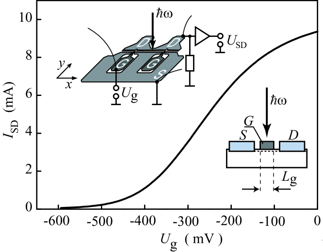
We studied commercially available GaAs/AlGaAs HEMTs with a gate length of 150 nm and a gate width of 280 m. Figure 1 shows the design of the transistors, where the disposition of source (S), drain (D) and two gate (G) pads is sketched. The transistor’s threshold voltage is obtained from the transfer characteristics, shown in Fig. 1, to approximately -440 mV. More detailed description of HEMT layers can be found in Ref. [transistor, ]. We also investigated Si-MODFETs with 150 nm and m.
The experiments have been performed applying a cw methanol laser as well as pulsed NH3, D2O and CH3F lasers JETP1982 ; physicaB99 as sources of radiation in the frequency range of THz. The cw laser operated at THz (wavelength m) with a power of about 20 mW cw . The NH3, D2O, CH3F lasers provided 100 ns pulses at 2 THz ( m), 1.1 THz ( m), 0.8 THz ( m), and 0.6 THz ( m) with an output power of about 10 kW Schneider2004 ; our6 . The incident radiation power was monitored by a photon drag reference detector JTPL1985 . The laser beam was focused onto the sample by a parabolic mirror with a focal length of 65 mm. Typical laser spot diameters varied, depending on the wavelength, from 1 to 3 mm. The spatial laser beam distribution had an almost Gaussian profile, checked with a pyroelectric camera Ziemann00 . In some experiments we used also a 95.5 GHz ( mm) Gunn diode as a cw source with a maximum output power of about 20 mW. No special antennas were used and the terahertz/microwave radiation was coupled to the device directly through bonding wires or metalization contact pads. The spatial distribution of the microwave radiation at the sample’s position, and, in particular, the efficiency of the radiation coupling to the sample, by, e.g., the bonding wires and metalization of contact pads, could not be measured. Thus, all microwaves data are given in arbitrary units. Both linear and circular polarized light experiments were performed. To study the detector response upon variation of the radiation polarization state /4 - and /2 - plates made of x-cut crystalline quartz were used. In the pulsed THz experiments, the photoinduced voltage, , was fed through an inverting input of an amplifier with a voltage amplification of 20 dB and a bandwidth of 300 MHz (rise time of about 1 ns) to a digital broadband 1 GHz-oscilloscope. In the cw experiments with the Gunn diode or gas laser sources, we used standard lock-in technique with a voltage amplification of 20 dB. The photoresponse was studied at different values of gate bias, . All experiments were performed at room temperature.
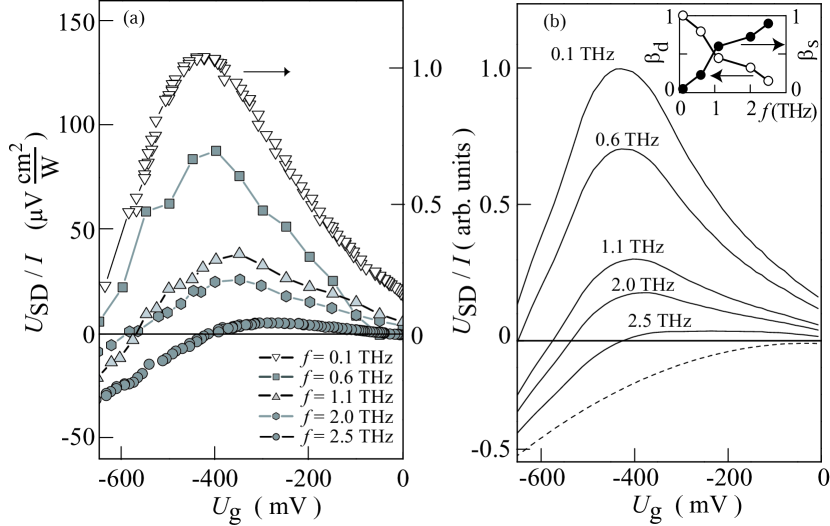
Results of experiments with linearly polarized light are summarized in Figs. 2(a) and 3. Figure 2(a) shows a gate voltage dependence of the HEMT’s photoresponse measured for different radiation frequencies in the range of 0.1 to 2.5 THz. For all used frequencies, the signal shows a maximum for a gate bias close to the threshold voltage, mV. With increasing frequency the magnitude of the maximum of the response decreases rapidly. The data show also that, at high frequencies, the signal switches its polarity at a certain gate bias. Note that the gate-bias of the inversion point diminishes with raising frequency. While a non-monotonic behavior of the signal, like observed for lower frequencies, is well known for FET detectors, the change of the response sign with increasing radiation frequency has not been reported so far. Moreover, our experiments revealed a peculiar polarization behavior of the photosignal, in particular, at high radiation frequencies and large negative voltages.
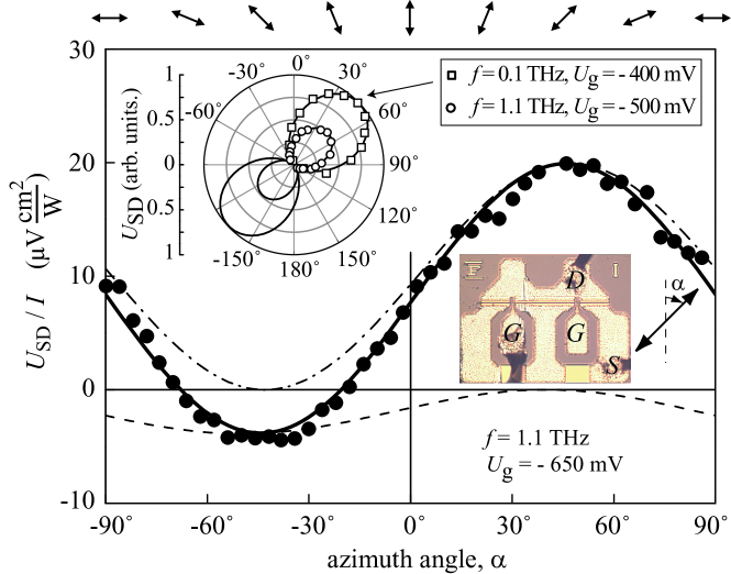
Sakowicz et al. Sak2010 have shown that at low frequencies the radiation is coupled to the transistor mainly by bonding wires, whereas at higher frequencies ( 100 GHz) the metalization of the contact pads plays the role of efficient antennas. Therefore, to interpret our experiments we represent the photoinduced signal as a sum of two contributions:
| (1) | |||||
with (, ) and (, ) being of opposite sign. Herein, is the azimuth angle defined in the inset of Fig. 3, and are the phase angles, depending on the special alignment/geometry of bonding wires and metalization pads. Below we show that this assumption allows to reproduce the experimental traces, see Fig. 3. At the lowest radiation frequency of 100 GHz, the signal is well described by Eq. (1) with the phase angle and the second contribution close to zero. These data are shown in the top left inset in Fig. 3. Comparison of the photovoltage distribution with the picture of the HEMT transistor (right inset in Fig. 3) reveals that the signal achieves a maximum value for the radiation polarization vector aligned roughly parallel to the line connecting the contact wires of the gate and drain. Disregarding the vanishingly small portion of the signal proportional to , this behavior corresponds to the photoresponse of conventional FET detectors with the incoming radiation coupled to the transistor channel only by the bonding wires. Almost the same result has been obtained for higher frequencies and relatively small gate voltages, see e.g. the data for THz and mV shown in top left inset of Fig. 3. For higher frequencies and large bias voltages, however, we observed that the magnitudes of and become comparable. An example of such a behavior is shown in Fig. 3 for 1.1 THz and -650 mV, together with the corresponding fits to Eq. (1). Note that the sign of and the value of the phase angle remain unchanged. The best fit is obtained for negative value of and , i.e. the maximum of this contribution is obtained for the polarization vector oriented almost perpendicular to the line connecting the contact wires of the gate and drain. Thus, the contribution to the photosignal given by the voltage could not result from the antenna coupling to the connecting wires and can be only attributed to the radiation coupling through the contact pads.
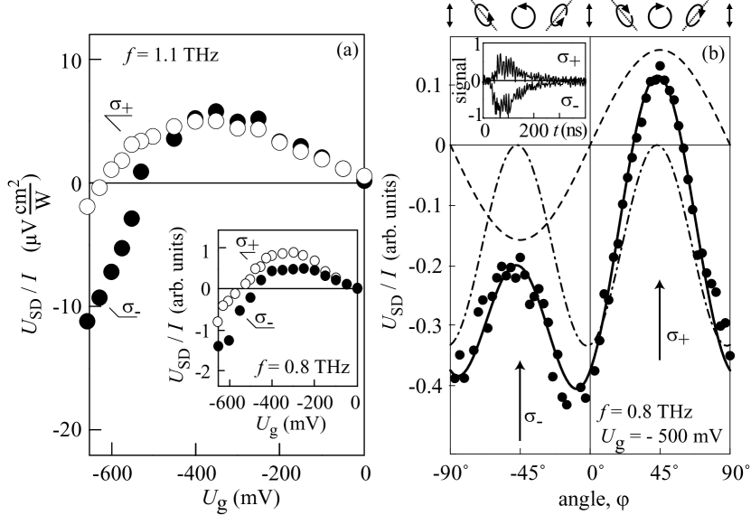
Besides the complex polarization dependence upon rotation of the linear polarization plane, we observed that the photoresponse depends on the radiation’s helicity. Fig . 4(a) shows versus the gate voltage measured for right- () and left- () handed circularly polarized radiation with frequencies and 1.1 THz. The data show that at relatively low bias voltages , for which the dominating contribution of the signal proportional to is detected, the photoresponse is insensitive to the radiation helicity. At higher negative bias voltages, however, the values and even the sign of the signal becomes different for and polarized radiation. By varying the radiation ellipticity we obtain a polarization behavior of the signal as shown Fig. 4(b) which can be well reproduced by the following equation:
with , , and as the fitting parameters. This equation shows that the photoresponse is caused by a superposition of i) the signal proportional to the degree of circular polarization (first term) and ii) signals determined by the degree of linear polarization of elliptically polarized light (second and third terms). Here, is the radiation electric field. The inset in Fig. 4(b) shows the typical photoresponse pulses for right- and left-handed circularly polarized radiation. A helicity dependent photoresponse was also observed for Si-MODFETs of similar design but the discussion of this data is out of scope of this paper.
III Theoretical background and discussion
In the following, we show that the observed photoresponse as well as its polarisation dependence can be well described in the frame of the generalized model of THz detection by FETs DS96 . The operation regime of the FET as a THz detector depends on the parameter , which determines whether plasma waves are excited () or not (). In our experimental conditions the value of is between 0.04 and 1 so that plasma oscillations are overdamped and the FET operates as a broadband detector. The channel length in the investigated transistors is much shorter than the wavelength, and the channel is mostly covered by the metallic gate. Hence, there is no direct interaction of the electromagnetic radiation with the electron gas in the channel. Therefore, the radiation is coupled to the channel through the source-gate and drain-gate contacts by effective antennas formed by the metallic contact pads and/or bonding wires. An ac current induced by the radiation at the source (or at the drain) will leak to the gate at a distance on the order of the leakage length
| (3) |
where is the conductivity of the channel and C is the gate-to-channel capacitance per unit length. If the is much larger than the leakage length , the photovoltage is generated in a region on the order of near the contact.
In the case when the radiation produces an ac voltage with an amplitude between the source and gate contacts, the photoresponse is given by D2010 :
| (4) | |||||
| (5) |
The prefactor in the expression for is valid for positive values of the gate voltage swing, , which are not too close to zero. In the vicinity of the threshold and in the subthreshold region this prefactor was calculated in Ref. DS96 . It depends on the dc gate leakage current as well as on the transistor impedance. The dependence on is universal. Experimentally, the photoresponse as a function of has a broad maximum around the threshold. The amplitude of the input ac voltage is related to the incoming radiation intensity and the antenna’s sensitivity as . Thus, the photoresponse can be presented in the form D2010
| (6) |
In order to interpret the experimental results, we assume that the radiation is fed to both, the source-gate and the gate-drain contacts. In other words, the coupling of the radiation to the transistor channel can be modeled by two effective antennas, one of them producing an ac voltage between source and gate (), and the other one between drain and gate (). As long as is much smaller than , there is no interference between the currents induced at opposite sides of the channel, and the corresponding contributions to the total photoresponse are independent. These contributions are obviously of opposite signs, resulting in a vanishing photoresponse for equal ac amplitudes. The total photoresponse is given by
| (7) |
where is the parameter describing the frequency dependence of the photoresponse, whereas and are frequency dependent sensitivities of the source-gate and drain-gate effective antennas, respectively. The functions and describe the gate bias dependences of the photoresponse generated at the source and drain sides of the channel.
The role of antennas can be played by contact wires as well as metallic contact pads. Our results show that at = 95.5 GHz the incoming radiation is coupled to the transistor channel by contact wires. This fact is in agreement with Ref. sakowicz08 ; Sak2010 where similar devices were studied. Indeed, we find that the photoresponse is optimal when the radiation polarization is aligned along the line connecting the gate and drain contact wires (see the right inset in Fig. 3). This demonstrates that at low frequencies the radiation is mostly coupled to the drain side of the channel. Hence, the upper curve in Fig. 2(a) can be attributed to the photoresponse generated at the drain side only, , i.e. (0.1 THz) = 1 and (0.1 THz) = 0. In contrast, at high frequencies, the radiation is expected to be coupled to the channel primarily through the contact metallic pads Sak2010 . This enables coupling to the source side of the channel which, obviously, should lead to an opposite sign of the signal. Indeed, the photoresponse at 2.5 THz is negative in most of the gate voltage range. Figure 2(b) shows calculated for different fitting parameters and . In order to determine the function we used the experimental dependence of the photoresponse on the gate voltage measured at THz. Function is presented by the dashed line in Fig. 2(b). In agreement with the above discussion it is assumed to be negative in the whole range of the gate voltage.
This choice of the functions and allows a good fit of photoresponse curves for all frequencies, see Fig. 2. The inset in Fig. 2 demonstrates that the increase of the radiation frequency consistently decreases the efficiency of the gate-drain antenna, , and increases the coupling by the source-gate antenna, footnote1 . Thus, at intermediate frequencies the photoresponse is a superposition of two signals generated at the drain and the source sides of the channel. This becomes also apparent in experiments with linear polarization of radiation. As seen in Fig. 3, at a frequency of 1.1 THz and mV, the polarization dependence of the photoresponse is well fitted by the sum of dot-dashed and dashed curves footnotex .
Now we turn to the observed helicity dependent photoresponse, and we show that it can just as well be understood using the described model of two effective antennas. So far we have assumed that the ac currents generated on both sides of the channel do not interfere. This corresponds to the case when the leakage length is sufficiently small compared to . If is of the order of there would be a region where the ac currents generated at the source and drain coexist. Then the resulting ac current will depend on their phase difference, . Such a phase difference appears when source and drain are excited by mutually orthogonal components of circularly (or elliptically) polarized radiation. As we have seen above this is the case in our experimental setup, where source and drain effective antennas show maximal sensitivity for polarization directions differing by about 90∘. Consequently, the ac currents generated at source and drain will have phase shift . It can be shown LifhitsDyakonov that, if is comparable to , Eq. (7) should be modified as follows:
| (8) | |||
where the last interference term is sensitive to the radiation’s helicity (sign of ). For linear polarization and , Eq. (III) reduces to Eq. (7). The characteristic length is frequency dependent, see Eq. (3), and can be estimated to 76 nm (0.8 THz) and 89 nm (1.1 THz). Thus, it is of the same order as the gate length, and the induced ac currents at the drain and source sides can interfere. As it follows from Fig. 2, for THz the contributions of source-gate and drain-gate antenna become equal at 565 mV, where . Thus, for this gate voltage only the interference term remains and the photoresponse should change its sign when the helicity of radiation is reversed. This is indeed what we observe, see Fig. 4(a). The pulse traces obtained for right- and left- handed circularly polarized radiation demonstrate that the transistor allows the time resolved detection of a fine structure of the laser pulses with short spikes of the order of nanoseconds, see the inset in Fig. 4(b). The response time of the transistor is determined by the time resolution of our setup, but it is 2 ns or less. The same response times were observed at . The time constant is given by the cut-off frequency which is 10 GHz. The practically achievable time resolution, however, is RC-limited by the design of the electric circuitry and by the bandwidth of cables and amplifiers.
IV Summary
To summarize, we demonstrate that for certain conditions high electron mobility transistors excited by terahertz laser radiation yield a photoresponse which depends on the radiation handedness, in particular may change its sign by reversing the circular polarization of radiation from right to left handed. The helicity dependent detection mechanism is interpreted in the frame of the generalized Dyakonov-Shur model, by taking into account the interference of the ac currents in the transistor channel and specific antenna design. We show that, (i) optimization of the transistor design and (ii) the proper choice of the gate voltage, for which response to the linear polarization vanishes, should allow constructing a detector element with the responsivity just proportional to the radiation helicity, i.e. to the corresponding Stokes parameter. Combining such a detector element with two conventional FETs yielding a response to the linearly polarized radiation and, consequently, to the two remaining Stokes parameters should permit the complete characterization of radiation polarization in an all-electric manner. By the proper choice of the gate voltage, such room temperature detectors can be tuned to any radiation frequency in the THz range and are characterized by a nanosecond time resolution. Finally, we would like to emphasize that the observed transistor photoresponse is by several orders of magnitude higher than that one observed for the photogalvanic effect considered for the all-electric detection of the radiation’s polarization state Ganichev07 ; Danilov09 . Thus, the field effect transistor is a valuable candidate as a polarization detector.
V Acknowledgements
We thank M.I. Dyakonov, V.V. Bel’kov, and V.Yu. Kachorovskii for useful discussions. This work was supported by the DFG via Project SFB 689, Applications Center ”Miniaturisierte Sensorik” (SappZ) of the Bavarian Government, the Linkage Grant of IB of BMBF at DLR. This work was supported by the CNRS through GDR-I project, by Region of Languedoc-Roussillon through the ”Terahertz Platform” project and by the ANR via the ”With” project. Y. M. M. acknowledges the financial help from the Ministry of Science and Innovation (project TEC2008-02281).
References
- (1) K. Sakai, Terahertz Optoelectronics (Springer, Berlin 2005).
- (2) S. D. Ganichev and W. Prettl, Intense Terahertz Excitation of Semiconductors (Oxford University Press, Oxford, 2006).
- (3) Terahertz Frequency Detection and Identification of Materials and Objects, eds. R.E. Miles, X. C. Zhang, H. Eisele, and A. Krotkus (Springer, Dordrecht, 2007).
- (4) Terahertz Science and Technology for Military and Security Applications, eds. D. L. Woolard, J. O. Jensen, and R. J. Hwu (World Scientific, Singapore, 2007).
- (5) Terahertz Spectroscopy: Principles and Applications (Optical Science and Engineering), ed. S.L. Dexheimer (CRC Press, Boca Raton, 2007).
- (6) Yun-Shik Lee, Principles of Terahertz Science and Technology (Springer, New York, 2008).
- (7) Xi-Cheng Zhang and Jingzhou Xu Introduction to THz Wave Photonics (Springer, New York, 2009).
- (8) D. Mittleman Sensing with Terahertz Radiation (Springer Series in Optical Sciences) (Springer, Berlin, 2010).
- (9) M. Dyakonov and M. S. Shur, IEEE Trans. Electron Devices 43, 380 (1996).
- (10) W. Knap, et al. Appl. Phys. Lett. 80, 3433 (2002).
- (11) W. Knap, V. Kachorovskii, Y. Deng, S. Rumyantsev, J.-Q. L , R. Gaska, M. S. Shur, G. Simin, X. Hu, M. Asif Khan, C. A. Saylor, and L. C. Brunel, J. Appl. Phys. 91, 9346 (2002).
- (12) W. Knap, Y. Deng,S. Rumyantsev and M. S. Shur, Appl.Phys. Lett. 81, 4637 (2002).
- (13) X. G. Peralta, S. J. Allen, M. C. Wanke, N. E. Harff, J. A. Simmons, M. P. Lilly, J. L. Reno, P. J. Burke, and J. P. Eisenstein, Appl. Phys. Lett. 81, 1627 (2002).
- (14) W. Knap, F. Teppe, Y. Meziani, N. Dyakonova, J. Lusakowski, F. Boeuf, T. Skotnicki, D. Maude, S. Rumyantsev and M. S. Shur, Appl. Phys. Lett. 85, 675 (2004).
- (15) E. A. Shaner, Mark Lee, M. C. Wanke, A. D. Grine, and J. L. Reno S. J. Allen, Appl. Phys. Lett. 87, 193507 (2005).
- (16) R. Tauk, F. Teppe, S; Boubanga, D. Coquillat, W. Knap, Y. M. Meziani, C. Gallon, F. Boeuf, T. Skotnicki, C. Fenouillet-Beranger, D. K. Maude, S. Rumyantsev, and M. S. Shur, Appl. Phys. Lett. 89, 253511 (2006).
- (17) M. Sakowicz, J. Łusakowski, K. Karpierz, M. Grynberg, W. Knap, and W. Gwarek, J. Appl. Phys. 104, 024519 (2008).
- (18) W. Knap, F. Teppe, N. Dyakonova, D. Coquillat and J usakowski, J. Phys.: Condens. Matter 20, 384205 (2008).
- (19) S. Kim, Jeramy D. Zimmerman, P. Focardi, A.C. Gossard, D.H. Wu, and M.S. Sherwin, Appl. Phys. Lett. 92, 253508 (2008).
- (20) D.B. Veksler, A.V. Muravjov, V.Yu. Kachorovskii, T.A. Elkhatib, K.N. Salama, X.-C. Zhang, and M.S. Shur, Solid-State Electron. 53, 571 (2009).
- (21) W. Knap, M. I. Dyakonov, D. Coquillat, F. Teppe, N.Dyakonova, M. Sakowicz, J. Łusakowski, K. Karpierz, G. Valusis, D. Seliuta, I. Kasalynas, A. El Fatimy, Y. Meziani, and T. Otsuji, J. Infrared Milli Terahz Waves 30, 1319 (2009).
- (22) G.C. Dyer, J.D. Crossno, G.R. Aizin, E.A. Shaner, M.C. Wanke, J.L. Reno and S.J. Allen, J. Phys.: Condens. Matter 21, 195803 (2009).
- (23) V. V. Popov, D. V. Fateev, T. Otsuji, Y. M. Meziani, D. Coquillat, and W. Knap, Appl. Phys. Lett. 99, 243504 , (2011).
- (24) F. Schuster , D. Coquillat, H. Videlier, M. Sakowicz, F. Teppe, L. Dussopt, B. Giffard, T. Skotnicki, and W. Knap, Opt. Express 19, 7827 (2011).
- (25) M. Sakowicz, J. Lusakowski, K. Karpierz, M. Grynberg, W. Gwarek, S.Boubanga, D.Coquillat, W. Knap, A. Shchepetov, and S. Bollaert, AIP Conf. Proc. 1199, 503 (2010).
- (26) S.D. Ganichev, E. L. Ivchenko, and W. Prettl, Physica E 14, 166 (2002).
- (27) Spin Physics in Semiconductors, edited by M. I. D’yakonov (Springer, Berlin 2008).
- (28) S.D. Ganichev, V. V. Bel’kov, Petra Schneider, E. L. Ivchenko, S.A. Tarasenko, W. Wegscheider, D. Weiss, D. Schuh, E.V. Beregulin and W. Prettl, Phys. Rev. B 68, 035319 (2003).
- (29) S.D. Ganichev, Petra Schneider, V. V. Bel’kov, E. L. Ivchenko, S.A. Tarasenko, W. Wegscheider, D. Weiss, D. Schuh, B. N. Murdin, P. J. Phillips, C. R. Pidgeon, D. G. Clarke, M. Merrick, P. Murzyn, E. V. Beregulin, and W. Prettl, Phys. Rev. B. (Rapid Communic.) 68, 081302 (2003).
- (30) E. Öjefors, A. Lisauskas, D. Glaab, H. G. Roskos, and U.R. Pfeiffer, J. Infrared Millimeter Terahertz Waves 30, 1269 (2009).
- (31) A. Lisauskas, U. Pfeiffer, E. Öjefors, P.H. Bolivar, D. Glaab, and H. G. Roskos, J. Appl. Phys. 105, 114511 (2009).
- (32) W. Knap, G. Valusis, J. Lusakowski, D. Coquillat, F. Teppe, N. Dyakonova, S. Nadar, K. Karpierz, M. Bialek, D. Seliuta, I. Kasalynas, and A. E. Fatimy, phys. status solidi C 6, 2828 833 (2009).
- (33) Fujitsu Microwave Semiconductor Databook (1999), Fujitsu Compound Semiconductor, Inc., 2355 Zanker Rd., San Jose, CA 95131-1138, USA.
- (34) S. D. Ganichev, S. A. Emel’yanov, and I. D. Yaroshetskii, Pis’ma Zh. Èksp. Teor. Fiz. 35, 297 (1982) [JETP Lett. 35, 368 (1982)].
- (35) S. D. Ganichev, Physica B 273-274, 737 (1999).
- (36) Z.D. Kvon, S.N. Danilov, N.N. Mikhailov, S.A. Dvoretsky, and S.D.Ganichev, Physica E 40, 1885 (2008).
- (37) P. Schneider, J. Kainz, S.D. Ganichev, V.V. Bel’kov, S.N. Danilov, M.M. Glazov, L.E. Golub, U. Rössler, W. Wegscheider, D. Weiss, D. Schuh, and W. Prettl, J. Appl. Phys. 96, 420 (2004).
- (38) S.D. Ganichev, S.N. Danilov, V.V. Bel’kov, S. Giglberger, S.A. Tarasenko, E.L. Ivchenko, D. Weiss, W. Jantsch, F. Schäffler, D. Gruber, and W. Prettl, Phys. Rev. B 75, 155317 (2007).
- (39) S. D. Ganichev, Ya. V. Terent’ev, and I. D. Yaroshetskii, Pis’ma Zh. Tekh. Fiz 11, 46 (1985) [Sov. Tech. Phys. Lett. 11, 20 (1985)].
- (40) E. Ziemann, S. D. Ganichev, I. N. Yassievich, V. I. Perel, and W. Prettl, J. Appl. Phys. 87, 3843 (2000).
- (41) M.I. Dyakonov, C.R. Physique 11, 413 (2010). See also arXiv:1103.4316v1.
- (42) It should be noted that here we compare only the shape of the photoresponse curves to establish the relative contributions of source and drain sides of the channel. The absolute value of the photoresponse depends also on the radiation power , which, for the large variety of the radiation sources used in our work, could not be compared properly for different frequencies varying over almost two decades.
- (43) Note that the first curve has a maximum when the polarization direction coincides with the line connecting the contact wires, i. e. it describes the photoresponse to the radiation coupled to drain side of the channel. The second one is of opposite sign and maximal when the polarization axis is turned by 97∘ with respect to the wires connecting line. This curve is attributed to the photoresponse caused by the radiation coupling to the source side of the channel.
- (44) M. Lifhits and M. Dyakonov, to be published.
- (45) S.D. Ganichev, J. Kiermaier, W. Weber, S.N. Danilov, D. Schuh, Ch. Gerl, W. Wegscheider, D. Bougeard, G. Abstreiter, and W. Prettl, Appl. Phys. Lett. 91, 091101 (2007).
- (46) S.N. Danilov, B. Wittmann, P. Olbrich, W. Eder, W. Prettl, L.E. Golub, E.V. Beregulin, Z.D. Kvon, N.N. Mikhailov, S.A. Dvoretsky, V.A. Shalygin, N.Q. Vinh, A.F.G. van der Meer, B. Murdin, and S.D. Ganichev, J. Appl. Physics 105, 013106 (2009).