Gap modification of atomically thin boron nitride by phonon mediated interactions.
Abstract
A theory is presented for the modification of bandgaps in atomically thin boron nitride (BN) by attractive interactions mediated through phonons in a polarizable substrate, or in the BN plane. Gap equations are solved, and gap enhancements are found to range up to 70% for dimensionless electron-phonon coupling , indicating that a proportion of the measured BN bandgap may have a phonon origin.
Introduction
The need for bandgaps in graphene on eV scales has led to a number of proposals, such as the use of bilayer graphene [1] creation of nanoribbons [2] and manipulation through substrates [3, 4]. Recently it has become possible to manipulate atomically thin layers of boron nitride (BN) and other materials with structure similar to graphene [5]. This may lead to a complimentary method of manipulating bandgaps to make digital transistors.
In low dimensional materials, strong effective electron-electron interactions can be induced via interaction between electrons confined to a plane and phonons in a polarizable neighboring layer [6]. Theory has shown that similar interactions account for the transport properties of graphene on polarizable substrates [7], and that sandwiching graphene between polarisable superstrates and gap opening substrates can cause gap enhancement [8]. This paper examines similar gap changes in atomically thin BN due to interactions mediated through substrates.
Model
Atomically thick hexagonal BN (h-BN) has similar chemistry to graphene: Bonding occurs through hybridization, and electrons with energies close to the chemical potential are in unhybridized orbitals [9]. A key difference is that the electronic charge is not completely screened by the hybridization, shifting orbitals by on N sites and on B sites. This shift is the dominant cause of a gap of order . Tight binding fits to ab-initio simulations of monolayer BN have established that the hopping, eV [10], with an estimate of eV. Experiments indicate larger gaps: bulk h-BN has eV [11], and monolayer h-BN has a gap of eV [12] corresponding to eV. There is significant variation in phonon energies, , in h-BN [13]. LA phonons energies range up to around 140meV at the M point, and TA phonons to around 110meV at the K point. Optical phonon energies range between 160meV and 200meV. Coupling, , between electrons and phonons in either a polarisable substrate, or the BN monolayer is possible and the corresponding Hamiltonian is,
| (1) |
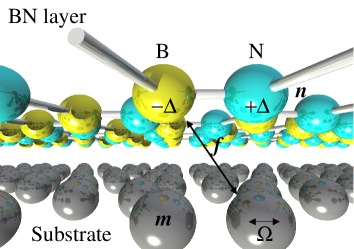
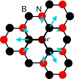
The Hamiltonian terms are shown schematically in Fig. 1 (left). creates electrons of spin on B sites and on N sites. Vectors are to atoms in the monolayer, and to atoms in the substrate. is the number operator for phonons. The Hamiltonian is also approximately valid for interactions in the plane, and Fig. 1 (right) shows the forces on ions from an increase in electron density at a B site. The largest forces are on the near-neighbor sites, so the effective interaction is mainly site diagonal (electrons on A sites self-interact through phonons on B sites and vice versa). The diagram indicates that the strongest interaction is between electrons and optical phonon modes.
For simplicity, I use the Holstein electron-phonon interaction, , which qualitatively captures the physics. There may be quantitative changes to the results for longer range Fröhlich interactions and from modulation of the electron-phonon interaction due to incommensurability of the substrate, which was estimated at around of the average value [8].
Gap equations and results
Low order perturbation theory is applicable for low phonon frequency and weak coupling. I derive a set of gap equations by symmetrizing the self energy,
The local approximation used here is a good starting point here because the modulated potential is large, and electrons are well localised. Off diagonal terms do not feature in the lowest order perturbation theory for the Holstein model since the interaction is site diagonal. is the quasi-particle weight and is the gap function. For bosonic quantities, and for fermions . is the temperature and and are integers.
The full Green function can be established using Dyson’s equation , leading to,
| (2) |
Substituting the expression for the Green function into the lowest order contribution to the self energy,
| (3) |
Here, the phonon propagator, , hence there are no off diagonal elements of the lowest order self energy. The use of a single averaged and here is consistent with a mean-field approximation. At half-filling, it is reasonable to assume that within the scope of the model, so that and . This leads to the gap equations,
| (4) |
| (5) |
where the full gap is . The density of states for a tight binding hexagonal lattice in the absence of a gap, , has the form given in Ref. [14]. The equations may be solved self consistently by performing a truncated sum on Matsubara frequencies.
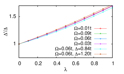
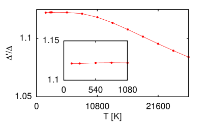
Gap and quasi-particle weight functions only have a weak Matsubara frequency dependence ( for , ). The local gap enhancement factors , are shown in Fig. 2 (left) for various , showing a modest increase of for . The enhancement factor increases slightly with decreasing but is essentially unchanged by modifications to phonon frequency and temperature for the parameter values used here. I also calculate the temperature dependence of the gap, Fig. 2 (right). For very large temperatures, where approaches , there is a drop in the gap size. For 8000 K, this levels off, and the gap becomes relatively constant.
Summary and conclusions
I have presented a theory for the modification of BN band-gaps by interaction with phonons. It is of interest to make comparison between the bandgaps of bulk h-BN, nanotubes, monolayer h-BN and the theory presented here. Measured bandgaps of bulk h-BN are of between 5.8eV [15] and 5.971eV [11], indicating that interaction between layers increases the bandgap, consistent with the theory here. The bulk gap is also higher than that for nanotubes (5eV) [16]. On the other hand, Song et al. [12] claim that the gap is reduced as BN thickness increases. The above discussion is presented with the caveat that the theory requires that hopping between the substrate and the BN monolayer is small. Interlayer hopping will affect the bandwidth and bandgap, and direct Coulomb interaction with strongly ionic substrates could also affect the band structure if the charge density at the surface of the substrate varies dramatically.
It is also of interest to estimate the magnitude of the bandgap modification due to electron-phonon interaction in isolated monolayers of BN. Ab-initio calculations have attempted to quantify the magnitude of the interaction between electrons and acoustic phonons for small momentum excitations [17]. Extrapolating the interaction, and taking a mean-field average (assuming mean momentum magnitude of ), the electron-phonon coupling can be estimated as , taking eV from Ref. [17], amu, . The mean energy of longitudinal acoustic phonons lies in the range meV, giving a range of , so the contribution of phonons to the bandgap is estimated as %. I would expect BN to have stronger interaction with optical phonons, since the pattern of distortions around an electronic defect is consistent with optical modes (see Fig. 1).
The BN gap is too wide for digital applications. Recently, it has become possible to manufacture silicene, an atomically thick layer of silicon with similar properties to graphene [18], so it may be possible to make GaAs or AlP analogues to BN. Smaller gaps could be available from those materials, which might be used to create tunable bandgaps for atomically thick transistors.
Acknowledgments
I acknowledge EPSRC grant EP/H015655/1 for funding and useful discussions with A. Ilie and A. Davenport.
References
- [1] McCann E, Fal’ko VI: Phys. Rev. Lett. 2006, 96:086805.
- [2] Brey L, Fertig HA: Phys. Rev. B 2006, 73:235411.
- [3] Zhou SY, Gweon GH, Fedorov AV, First PN, Heer WAD, Lee DH, Guinea F, Neto AHC, Lanzara A: Nature Materials 2007, 6:770.
- [4] Enderlein C, Kim YS, Bostwick A, Rotenberg E, Horn K: New J. Phys. 2010, 12:033014.
- [5] Novoselov KS, Jiang D, Schedin F, Booth TJ, Khotkevich VV, Morozov SV, Geim AK: Proc. Natl. Acad. Sci. U.S.A. 2005, 102:10451.
- [6] Alexandrov AS, Kornilovitch PE: J. Phys.: Condens. Matter 2002, 14:5337.
- [7] Fratini S, Guinea F: Phys. Rev. B 2008, 77:195415.
- [8] Hague J: Phys. Rev. B 2011, 84:155438.
- [9] Alem N, Erni R, Kisielowski C, Rossell M, Gannett W, Zettl A: Phys. Rev. B 2009, 80:155425.
- [10] Ribeiro RM, Peres NMR: Phys. Rev. B 2011, 83:235312.
- [11] Watanabe K, Taniguchi T, Kanda H: Nat. Mater. 2004, 3:404.
- [12] Song L, Ci L, Lu H, Sorokin P, Jin C, Ni J, Kvashnin A, Kvashnin D, Lou J, Yakobson B, Ajayan P: Nano Lett. 2010, 10:3209.
- [13] Serrano J, Bosak A, Arenal R, Krisch M, Watanabe K, Taniguchi T, Kanda H, Rubio A, Wirtz L: Phys. Rev. Lett. 2007, 98:095503.
- [14] Neto AHC, Guinea F, Peres NMR, Novoselov KS, Geim AK: Rev. Mod. Phys. 2009, 81:109.
- [15] Zunger A, Katzir A, Halperin A: Phys. Rev. B 1976, 13:5560.
- [16] Terauchi M, Tanaka M, Matsumoto T, Saito Y: J. Electron Microscopy 1998, 47:319.
- [17] Bruzzone S, Fiori G: Appl. Phys. Lett 2011, 99:222108.
- [18] Padova PD, Quaresima C, Ottaviani C, Sheverdyaeva P, Moras P, Carbone C, Topwal D, Olivieri B, Kara A, Oughaddou H, Aufray B, Lay GL: Appl. Phys. Lett. 2010, 96:261905.


