Transport Properties of Graphene Nanoroads in Boron-Nitride Sheets
Abstract
We demonstrate that the one-dimensional (1D) transport channels that appear in the gap when graphene nanoroads are embedded in boron-nitride (BN) sheets are more robust when they are inserted at AB/BA grain boundaries. Our conclusions are based on ab-initio electronic structure calculations for a variety of different crystal orientations and bonding arrangements at the BN/C interfaces. This property is related to the valley-Hall conductivity present in the BN band structure and to the topologically protected kink states that appear in continuum Dirac models with position dependent masses.
keywords:
h-Boron Nitride, Graphene ribbon, 1D conducting state, Kink State, Ballistic TransportInternational Center for Quantum Materials, Peking University, Beijing 100871, China Metallic transport channels appear at the edges, surfaces, and interfaces of two and three dimensional bulk insulators when a bulk topological index changes value as the interface region is crossed. 1, 2, 3, 4, 5, 6, 7, 8, 9, 10 This property can provide transport channels in otherwise insulating materials. The metallic states possess an internal structure related to their sense of propagation which leads to special transport properties including zero bend resistance at sharp turns in the current propagation trajectory, pseudospin memory, and suppressed backscattering. 7
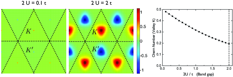
In this Letter we show that two-dimensional hybrid structures consisting of graphene nanoroads 13 (See 1) embedded in hexagonal boron nitride (BN) sheets can be an attractive host for topologically assisted one-dimensional (1D) transport channels. Our study is motivated by the observation that the -bands of BN are similar to those of a graphene sheet, except that the honeycomb sublattices have different -electron site energies. (The electrostatic potential is more attractive on the higher-Z N atom sites). Because valence band states near the and Brillouin-zone corners are strongly localized on sites whereas those elsewhere in the Brillouin-zone are divided more evenly, the bands of BN contribute with valley Hall conductivities and associated Berry curvatures of opposite signs near and whose continuum model expression is given by where is the momentum measured from a Dirac point, is the valley, is the lattice constant of the honeycomb lattice and is the band gap. 14. If the B-site vs. N-site potential difference was small, these Berry curvatures would be strongly concentrated near the BZ corners [see 2].
Indeed, in the graphene case it is known that electronic properties in systems with sublattice-staggered potentials that are weak compared to the -band width can be described using a two-dimensional massive Dirac equation. Under these circumstances Dirac-equation continuum models are valid and predict one-dimensional (1D) localized states along lines where the sublattice-staggered potential (the Dirac-equation mass) changes sign.3, 4 In the closely related bilayer5, 6, 7 and multilayer6 graphene cases, the sublattice staggered potentials are readily generated experimentally by applying an electric field across the layers and varied spatially by appropriately arranging external gate voltages. In the single-layer case, however, it has not been obvious how the sublattice-staggered potentials could be realized, although gaps may be present with a lattice matched BN substrate 11 or when gate potential profiles are carefully correlated with strains 12. This work is motivated by the idea that the difference between B-atom and N-atom potentials in BN provides the desired staggered potential. Of course the staggered potential is not weak in the case of a BN crystal, so that expectations based on massive Dirac continuum models must be checked by ab initio electronic structure calculations.
The topological index that is inherent in BN bands can be viewed as a valley Hall effect since each valley separately supports half integer quantum Hall effects of opposite sign, or at least does in the limit that the potential difference is small compared to the -band width. The properties that we discuss below are therefore closely related to the simple momentum space Berry curvature pattern in the bands of BN sheets. Hybrid BN/graphene systems of the type we study occur naturally in patched sheets containing a mixture of atomically thin graphene and BN, 15 and have recently become a subject of great interest, 16, 13, 17, 18, 19, 20, 21, 22, 23, 24, 25, 29, 26, 27, 28, 29, 30, 31, 32, 33 as the basis of a possible strategy for controlling graphene system band gaps. In this work we show that the properties of the transport channels formed by graphene nanoroads in BN strongly depend on the valley Hall effect of the surrounding material.
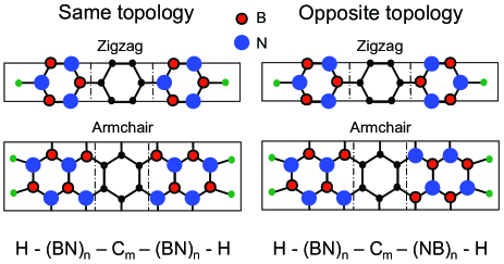
The simplest graphene nanoroad geometries have C/BN interfaces with crystallographic orientations along the zigzag and armchair directions. The unit cells considered in our ab initio calculation are illustrated in 1. In each case a graphene nanoribbon is flanked on the left and right by BN sheets with B and N atoms either on the same or opposite sublattices. When the two different BN fragments can be joined seamlessly preserving the crystalline B and N atom sequences upon carbon atom removal, as in the cases illustrated in the left panels of 1, the BN sheets on left and right have valley Hall conductivities of the same sign and we will say that they have the same topology. The right and center panels show junctions in which the BN sheets on opposite sides of the graphene nanoroad have opposite valley Hall conductivities. We will refer to these configurations as having opposite topologies. When the carbon atoms are removed, joining the BN fragments would in this case require BB or NN bond. As shown in 3, a difference in the topology of the BN sheet arrangement on the nanoroad shoulders invariably leads to a qualitative change in nanoroad quasi-1D band structure.
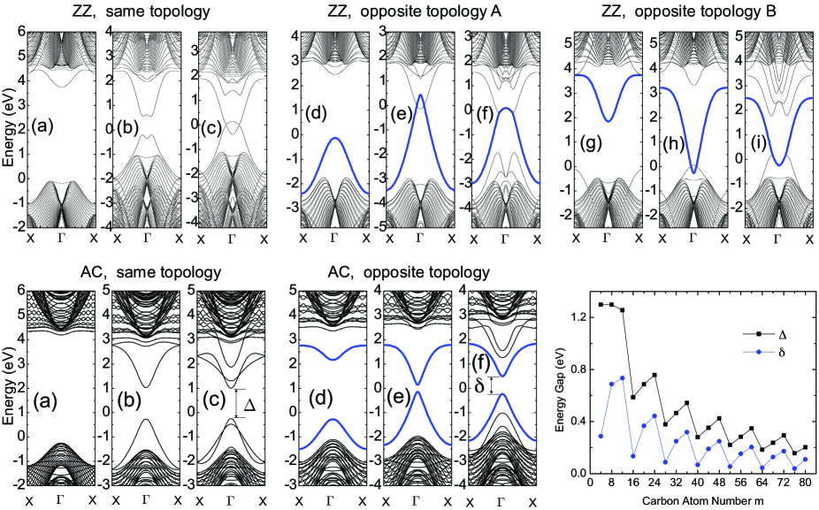
The indices and in 3 represent respectively the number of BN and carbon atoms in the 1D unit cell. The width of the BN fragment, specified by the index , plays a minor role in mid-gap state properties. We begin by discussing results for zero, one, and three hexagon width zigzag nanoroads presented in the upper panels of 3. The zero width cases illustrates the electronic structure of seamless BN nanoribbons with atoms of BN, and therefore a width of 86 nm. The large band gap of 4 is comparable to that of bulk BN. There is a notable lack of particle-hole symmetry in the band structure, which is partly due to the difference between B and N site potentials mentioned previously but cannot be captured by a nearest neighbor tight-binding model. We are mainly interested in the mid-gap states which emerge when a graphene nanoroad is embedded in the BN sheet. As expected on the basis of the properties of pure graphene nanoribbons, we find that zigzag graphene nanoroads do have strongly reduced gaps because of the presence of zigzag edge states.36, 37, 38 There is still however a topology sensitive feature; in the opposite topology case a mid-gap state appears that is peaked near the center of the nanoroad, rather than at its edges, with some penetration into the BN region. This state is indicated by blue shading in Figs. 3(d) to 3(i). We view this state as the lattice remnant of the mass-reversal (kink) state which would appear in the opposite topology case if the staggered potential was weak and the continuum model applied. Even in the absence of carbon atoms its appearance reduces the energy gap by approximately 2 eV. If the continuum model was accurate there would be opposite velocity kink states associated with the and valleys and the gap would disappear entirely.
Although gaps are absent for wide nanoroads in both like cases, the additional kink state present for opposite topologies closes the gap already at one hexagon width in the opposite topology case. For same topology configurations, the gaps are closed because the states that are most strongly localized at the edge are shifted in opposite directions by coupling to the BN shoulders. 38 For inverted topology, since the same type of atoms N or B are attached at both edges of the graphene nanoroad, we see a shift of onsite energies at the edge sites in the same direction, upwards for N atom bonds and downwards for B atom bonds. In this case the states closing the band gap have kink-state character and are spread widely over the C atoms of the nanoroad, and with some penetration into the BN region. 7
We now turn to armchair nanoroads. In ribbons this orientation does not support metallic edge states 40, and instead yields gaps which scale as the inverse ribbon width. Continuum model considerations suggest that reversed topology would lead to vanishing gaps for all widths.6, 7 The band structures in the lower panel of 3 demonstrate that there are gaps in the reversed topology case, but that the gaps are much smaller than in the same topology case. The magnitude of the small avoided crossing gap between opposite velocity kink states at shows the same oscillatory decline as a function of ribbon width that has been heavily studied in ribbons.39, 40 The gap reaches a value as large as 0.75 eV for armchair single-hexagon nanoroads. It is noteworthy that this avoided crossing is always smaller than the finite-size gap in either nanoribbons of the same width or same topology nanoroads, a fact that allows the kink channels to become the main current conducting path when the Femi level of the system is adequately shifted. The same topology and opposite topology gaps, and , are plotted as a function of nanoroad width in the bottom right panel of 3.
Zigzag graphene nanoroads have bearded interfaces terminations when they have an odd number of carbon atoms or non modulo 4 even integer number of C atoms in the unit cell.36, 37 These interfaces are not expected to be common in experimental systems because of stability considerations. A combination of zigzag and armchair fragments 35 are more abundant than bearded configurations with repeated dangling atoms. Bearded edges lead to more complicated band structures that we discuss further in the supplementary information, but generally preserve the tendency toward greater conduction in the opposite topology case.
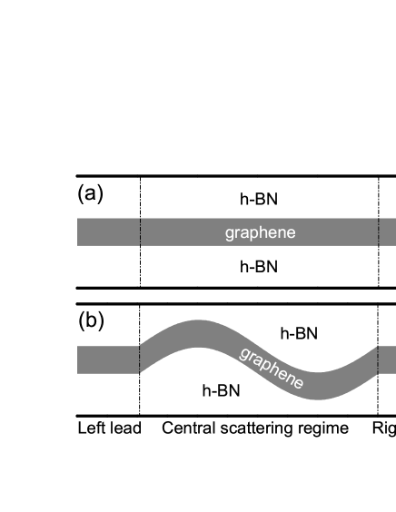
To address the influence of topology on nanoroad transport, we consider a two-terminal geometry with a central scattering region containing nanoroads that are either straight, or curved with both armchair and zigzag segments [See 4]. In our model, the source and drain electrodes are semi-infinite zigzag graphene nanoroads. The central scattering region contains 9660 lattice sites and the nanoroad width is fixed at 32 carbon atoms. The BNC nanoroad system is modeled using a nearest neighbor tight-binding Hamiltonian of the form
| (1) |
where () is a -orbital creation (annihilation) operator for an electron at the site , and are the BN -orbital site energies on the and subllices, and is the nearest neighbor hopping energy for both graphene and h-BN. We introduce a staggered AB sublattice potential to describe the site energy differences between B and N sublattices of h-BN, i.e. . Here, =‘’ defines the crystal topology of the h-BN regions in the graphene nanoroad. measures the strength of the staggered potential, and for the purposes of this illustrative calculation we have assumed it to be .
The temperature conductance from the left lead to the right lead can be calculated using the multi-probe Landauer-Büttiker formula: 41
| (2) |
where are the retarded and advanced Green functions of the central scattering region. The quantity is a linewidth function describing the coupling between left/right-lead and the central region and is obtained by calculating the self-energy of left/right-lead using a variant transfer matrix method. 42, 43, 44
5 plots conductance as a function of Fermi energy for the straight (zigzag-edged) and curved BNC nanoroads. In panel (a), the crystal topologies are the same in upper and lower h-BN regions. We observe that the conductance of the straight BNC nanoroad is quantized to be (). The conductance plotted here is per spin, so that the even conductance values can be attributed to the presence of ballistic states that are localized at both edges. The nanoribbon finite size effect for this nanoroad width produces a small band gap with vanishing conductance near the charge neutrality point. When the graphene nanoroad becomes curved in the central regime, disorder produces backscattering which supresses the conductance below the quantized value.
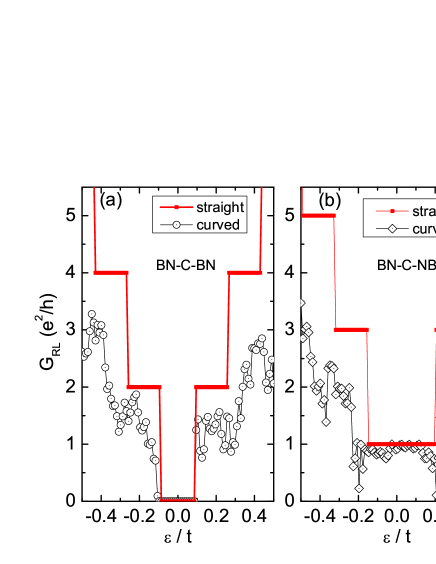
The case of opposite BN shoulder topologies is illustrated in 5(b). In this case the conductance rule for straight BNC nanoroads is changed to () as shown in 5(b). This change reflects the addition of a topologically supported kink state. For the curved reversed topology nanoribbon, the conductance does not decrease substantially in the region near the charge neutrality point where the only remaining channel is the kink state. Near the neutrality point the conductances show a surprising plateau feature with minor fluctuations that may be suppressed further by increasing the width of the graphene nanoroad. This finding strongly reflects the robustness of the crystal topology induced 1D topological conducting state against BNC nanoroad bends and is consistent with the finding of the zero bend resistance for 1D topological confinement states in gated bilayer graphene.7
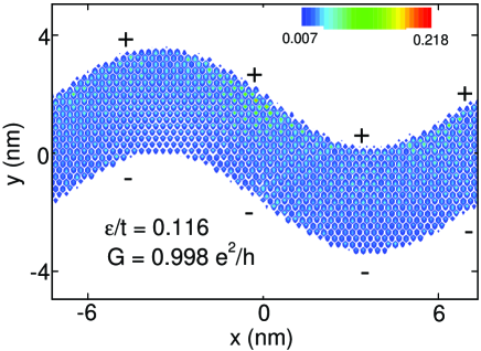
To visualize the 1D topological conducting channel, we can evaluate the position dependence of its local density of states (LDOS) of the current originating from lead using
| (3) |
Here is the Fermi energy. In 6, we plot the LDOS distribution of the topologically assisted conducting channel from the left lead into a snake-shaped BNC nanoroad. Our calculation shows that it is localized across the graphene atomic sites with only a small portion on the interface between h-BN and graphene. The transport calculations for the straight and curved nanoroad geometries confirms that the kink states picture remains essentially valid even when both zigzag and armchair edges are simultaneously present. The almost ballistic transport is preserved in spite of irregular bonds at the graphene/BN interfaces.
In summary, we have shown that graphene nanoroads embedded in BN sheets host kink-like transport channels when surrounded by opposite topology BN fragments. Transmission by the kink-states is topologically assisted and nearly perfect even when the graphene nanoroad is curved and has irregular edges consisting of combinations of both for zigzag and armchair edges.
1 Calculation Details
The self-consistent ab-initio calculations were carried out using the PAW-LDA parametrization of the exchange correlation functional in a plane wave basis code, as implemented in Quantum Espresso. 45 We used the 1.443 Angstrom for the separation between neighboring B, N and C atoms and 1.09 for BH and NH separations. These values are consistent with optimized lattice constants obtained from total energy minimization. Relaxation to obtain a final crystal geometry with atomic forces below Angstrom had a negligible effect in modifying the interatomic distances and band structures. For our nanoroad calculations in ribbon geometries we used 30, 1 and 1 k-points in the , and directions, and a plane wave energy cutoff of 60 Ry. The vacuum separation distances between supercell repeated nano ribbons was set to in both and directions.
This work was supported by NSF (DMR 0906025), NRI-SWAN, Welch Foundation (TBF1474, F-1255), DOE (DE-FG03-02ER45958, Division of Materials Science and Engineering), and Texas Advanced Research Program. We gratefully acknowledge the computation resources and assistance provided by the Texas Advanced Computing Center. {suppinfo} We have also attached a supporting information material for a more detailed understanding of our work.
References
- 1 Heeger A. J.; Kivelson S.; Schrieffer J. R.; Su W.-P. Rev. Mod. Phys. 1988, 60, 781.
- 2 Volovik G. E., ‘The Universe in a Helium Droplet’, Oxford University Press (2003).
- 3 Semenoff G. W.; Semenoff V.; Zhou F. Phys. Rev. Lett. 2008, 101, 087204.
- 4 Yao W.; Yang S. A.; Niu Q. Phys. Rev. Lett. 2009, 102, 096801.
- 5 Martin I.; Blanter Ya. M.; Morpurgo A. F. Phys. Rev. Lett. 2008, 100, 036804.
- 6 Jung J.; Zhang F.; Qiao Z. H.; MacDonald A. H. Phys. Rev. B 2011, 84, 075418.
- 7 Qiao Z. H.; Jung J.; Niu Q.; MacDonald A. H. Nano Lett. 2011, 11 (8), 3453.
- 8 Killi M.; Wei T.-C.; Affleck I.; Paramekanti A. Phys. Rev. Lett. 2010, 104, 216406.
- 9 Killi M.; Wu S.; Paramekanti A. Phys. Rev. Lett. 2011, 107, 086801.
- 10 Wu S.; Killi M.; Paramekanti A. E-print arXiv:1202.1441 (2012).
- 11 Giovannetti G.; Khomyakov P. A.; Brocks G.; Kelly P. J.; van den Brink J.; Physl Rev. B 2007, 76, 073103.
- 12 Low T., Guinea F., and Katsnelson M. I., Phys. Rev. B 2011, 83, 195436.
- 13 Bhowmick S.; Singh A. K.; Yakobson B. I. J. Phys. Chem. C 2011, 115, 9889.
- 14 Xiao D.; Yao W.; and Niu Q., Phys. Rev. Lett. 2007, 99, 236809.
- 15 Ci L.; Song L.; Jin C.; Jariwala D.; Wu D.; Li Y.; Srivastava A.; Wang Z. F.; Storr K.; Balicas L.; Liu F.; Ajayan P. M. Nat. Mat. 2010, 9, 430.
- 16 Rubio A. Nat. Mat. 2010, 9, 379.
- 17 Seol G.; Guo J. App. Phys. Lett. 2011, 98, 143107.
- 18 Shinde P. P.; Kumar V. Phys. Rev. B 2011, 84, 125401.
- 19 Pruneda J. M. Phys. Rev. B 2010, 81, 161409(R).
- 20 Li J.; Shenoy V. B. Appl. Phys. Lett. 2011, 98, 013105.
- 21 Liu Y.; Bhowmick S.; Yakobson B. I. Nano Lett. 2011, 11, 3113.
- 22 Ding Y.; Wang Y.; Ni J. Appl. Phys. Lett. 2009, 95, 123105.
- 23 Liu Y.; Wu X.; Zhao Y.; Zeng X. C.; Yang J. J. Phys. Chem. C 2011, 115, 9442.
- 24 Fan Y.; Zhao M.; Zhang X.; Wang Z.; He T.; Xia H.; Liu X. J. Appl. Phys. 2011, 110, 034314.
- 25 Lam K.-T.; Lu Y.; Feng Y. P.; Liang G. Appl. Phys. Lett. 2011, 98, 022101.
- 26 Berseneva N.; Krasheninnikov A. V.; Nieminen R. M. Phys. Rev. Lett. 2011, 107, 035501.
- 27 Ramasubramaniam A.; Naveh D. Phys. Rev. B 2011, 84, 075405.
- 28 Obodo K. O.; Andrew R. C.; Chetty N. Phys. Rev. B 2011, 84, 155308.
- 29 Manna A. K.; Pati S. K. J. Phys. Chem. C 2011, 115, 10842.
- 30 Song L. et al., E-print arXiv:1105.1876 (2011).
- 31 Modarresi M.; Roknabadi M. R.; Shahtahmasbi N. Physica E 2011, 43 (9), 1751.
- 32 Qiu M.; Liew K. M. J. Appl. Phys. 2011, 110, 064319.
- 33 Cao T.; Feng J.; Wang E. G. Phys. Rev. B 2011, 84, 205447.
- 34 Wakabayashi K. Phys. Rev. B 1999, 59, 8271.
- 35 Jia X. et al. Science 2009, 323, 1701.
- 36 Fujita M.; Wakabayashi K.; Nakada K.; Kusakabe K. J. Phys. Soc. Jpn. 1996, 65, 1920.
- 37 Nakada K.; Fujita M.; Dresselhaus G.; Dresselhaus M. S. Phys. Rev. B 1996, 54, 17954.
- 38 Jung J.; Pereg-Barnea T.; MacDonald A. H. Phys. Rev. Lett. 2009, 102, 227205.
- 39 Son Y.-W.; Cohen M. L.; Louie S. G. Phys. Rev. Lett. 2006, 97, 216803.
- 40 Brey L.; Fertig H. A. Phys. Rev. B 2006, 73, 235411.
- 41 Datta S., ‘Electronic Transport in Mesoscopic Systems’, Cambridge University Press (1995).
- 42 López Sancho M. P.; López Sancho J. M.; Rubio J. J. Phys. F: Met. Phys. 1984, 14, 1205.
- 43 Qiao Z. H.; Wang J. Nanotech. 2007, 18, 435402.
- 44 Wang J.; Guo H. Phys. Rev. B 2009, 79, 045119.
- 45 Giannozzi P. et al., http://www.quantum-espresso.org.